UCC5672
SLUS414B - FEBRUARY 2000 - REVISED MARCH 2002
FEATURES
∑ Auto Selection Multi-Mode Single
Ended or Low Voltage Differential
Termination
∑ 2.7V to 5.25V Operation
∑ Differential Failsafe Bias
∑ Built-in SPI-3 Mode Change Filter/
Delay
∑ Meets SCSI-1, SCSI-2, Ultra2 (SPI-2
LVD), Ultra3/Ultra160 (SPI-3) and
Ultra320 (SPI-4) Standards
∑ Supports Active Negation
∑ 3pF Channel Capacitance
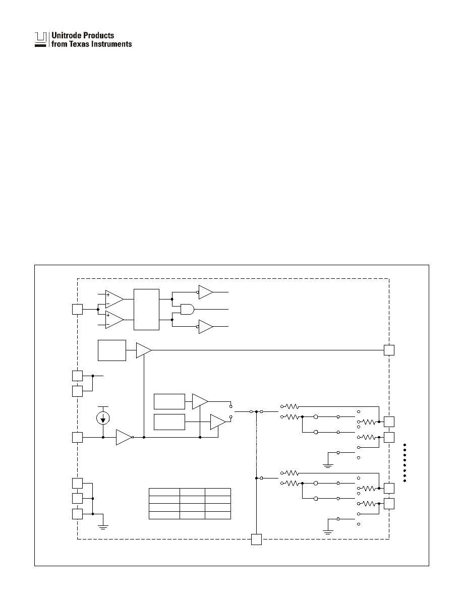
Multimode (LVD/SE) SCSI 9 Line Terminator
1
27
16
DIFSENS
DIFSENS
REF 1.3V
ENABLE
3
L1≠
52
2
L1+
52
L9≠
L9+
56mV
+
≠
56mV
≠
+
124
110
SE GROUND
SWITCH
26
52
25
52
56mV
+
≠
56mV
≠
+
124
110
SE GROUND
SWITCH
REG
17
DIFFB
0.6V
2.1V
FILTER/
DELAY
28
TRMPWR
TRMPWR
LVD REF
1.25V
SOURCE/SINK
REGULATORS
SE REF
2.7V
ENABLE
SW1
10
µA
22
6
HS/GND
HS/GND
14
GND
13
DISCNCT
SE
DISCNCT
HPD
LVD
UP
OPEN
DOWN
DOWN
DOWN
UP
OPEN
OPEN
MODE
SW1
OTHER
SWITCHES
HPD
LVD
SE
BLOCK DIAGRAM
UDG-99125
DESCRIPTION
The UCC5672 Multi-Mode Low Voltage Differential and Single Ended Ter-
minator is both a single ended terminator and a low voltage differential ter-
minator for the transition to the next generation SCSI Parallel Interface
(SPI-3). The low voltage differential is a requirement for the higher speeds
at a reasonable cost and is the only way to have adequate skew budgets.
The automatic mode select/change feature switches the terminator be-
tween Single Ended or LVD SCSI Termination, depending on the bus
mode. If the bus is in High Voltage Differential Mode, the terminator lines
transition into a High Impedance state.
The UCC5672 is SPI-4, SPI-3, SPI-2, and SCSI-2 compliant. This device
is offered in a 28 pin TSSOP package to minimize the footprint. The
UCC5672 is also available in a 36 pin MWP package.
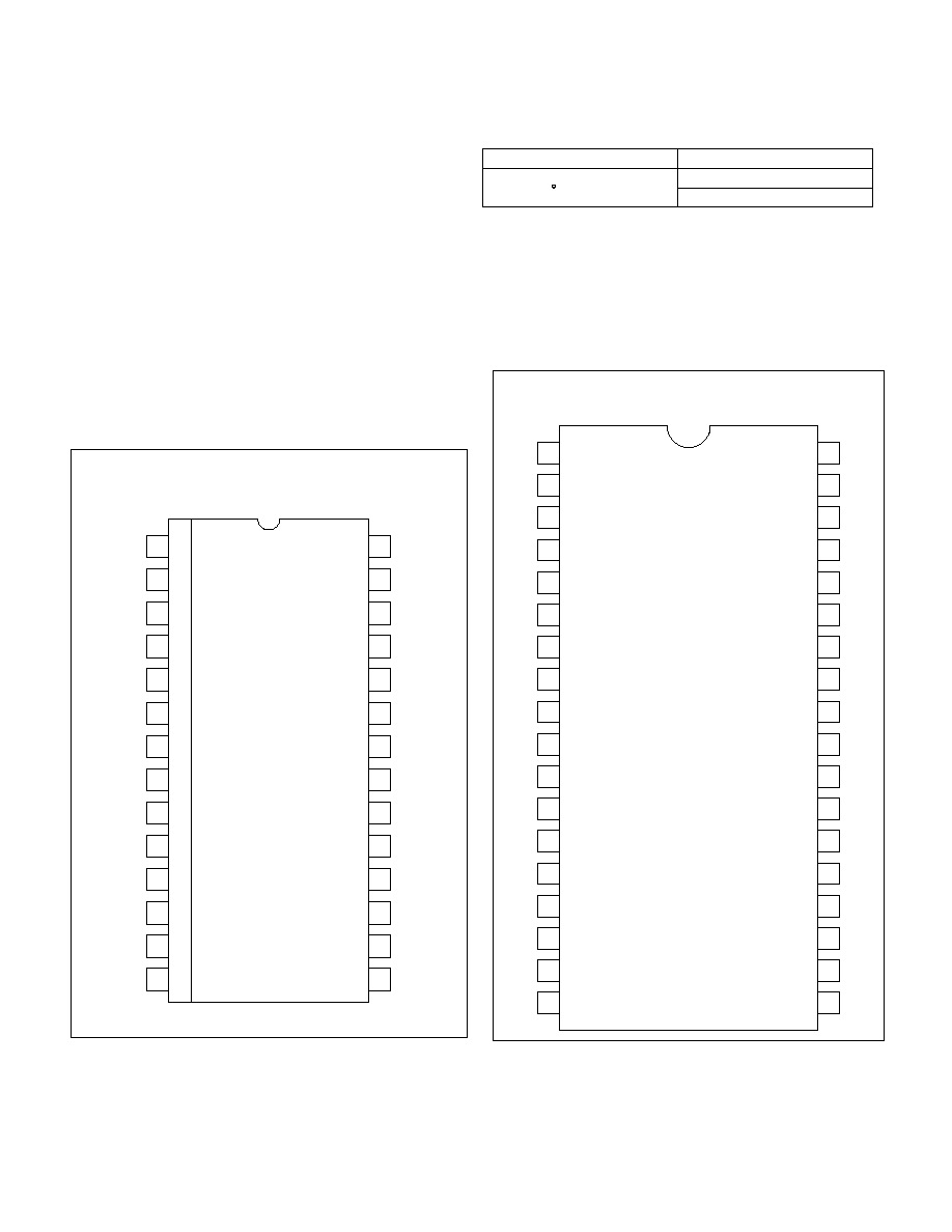
Note: Indicated pinout is for 28 pin TSSOP package.
2
UCC5672
ABSOLUTE MAXIMUM RATINGS
TRMPWR Voltage . . . . . . . . . . . . . . . . . . . . . . . . . . . . . . . . . 6V
Signal Line Voltage . . . . . . . . . . . . . . . . . . . . . . . . . . . 0V to 5V
Storage Temperature . . . . . . . . . . . . . . . . . . . ≠65∞C to +150∞C
Junction Temperature . . . . . . . . . . . . . . . . . . . ≠55∞C to +150∞C
Lead Temperature (Soldering, 10sec.) . . . . . . . . . . . . . +300∞C
All voltages are with respect to GND. Currents are positive into,
negative out of the specified terminal. Consult Packaging Sec-
tion of the Databook for thermal limitations and considerations
of packages.
RECOMMENDED OPERATING CONDITIONS
TRMPWR Voltage . . . . . . . . . . . . . . . . . . . . . . . . 2.7V to 5.25V
DIFFB
L6+
L8≠
L8+
L7≠
TRMPWR
L1+
L4≠
L3+
L4+
L1≠
L2+
L2≠
REG
L3≠
DIFSENS
L7+
L6≠
L5+
GND
14
13
12
11
10
9
8
7
6
5
4
3
2
1
15
16
17
18
19
20
21
22
23
24
25
26
27
28
L5≠
N/C
DISCNCT
L9≠
L9+
TRMPWR
HS/GND
HS/GND
CONNECTION DIAGRAM
L3+
HS/GND
L9≠
L9+
L8≠
TRMPWR
N/C
N/C
HS/GND
L2≠
HS/GND
L1+
L1≠
L2+
REG
HS/GND
L3≠
L8+
HS/GND
HS/GND
L4+
L4≠
14
13
12
11
10
9
8
7
6
5
4
3
2
1
23
24
25
26
27
28
29
30
31
32
33
34
35
36
18
17
16
15
DIFF B
N/C
DIFSENS
19
20
21
22
L5+
L5≠
DISCNCT
GND
L7≠
L7+
L6≠
L6+
N/C
N/C
N/C
TSSOP-28 (TOP VIEW)
PWP Package
QSOP-36 (TOP VIEW)
MWP Package
T
A
Packaged Devices
0 C to 70∞C
UCC5672MWP
UCC5672PWP
AVAILABLE OPTIONS
3
UCC5672
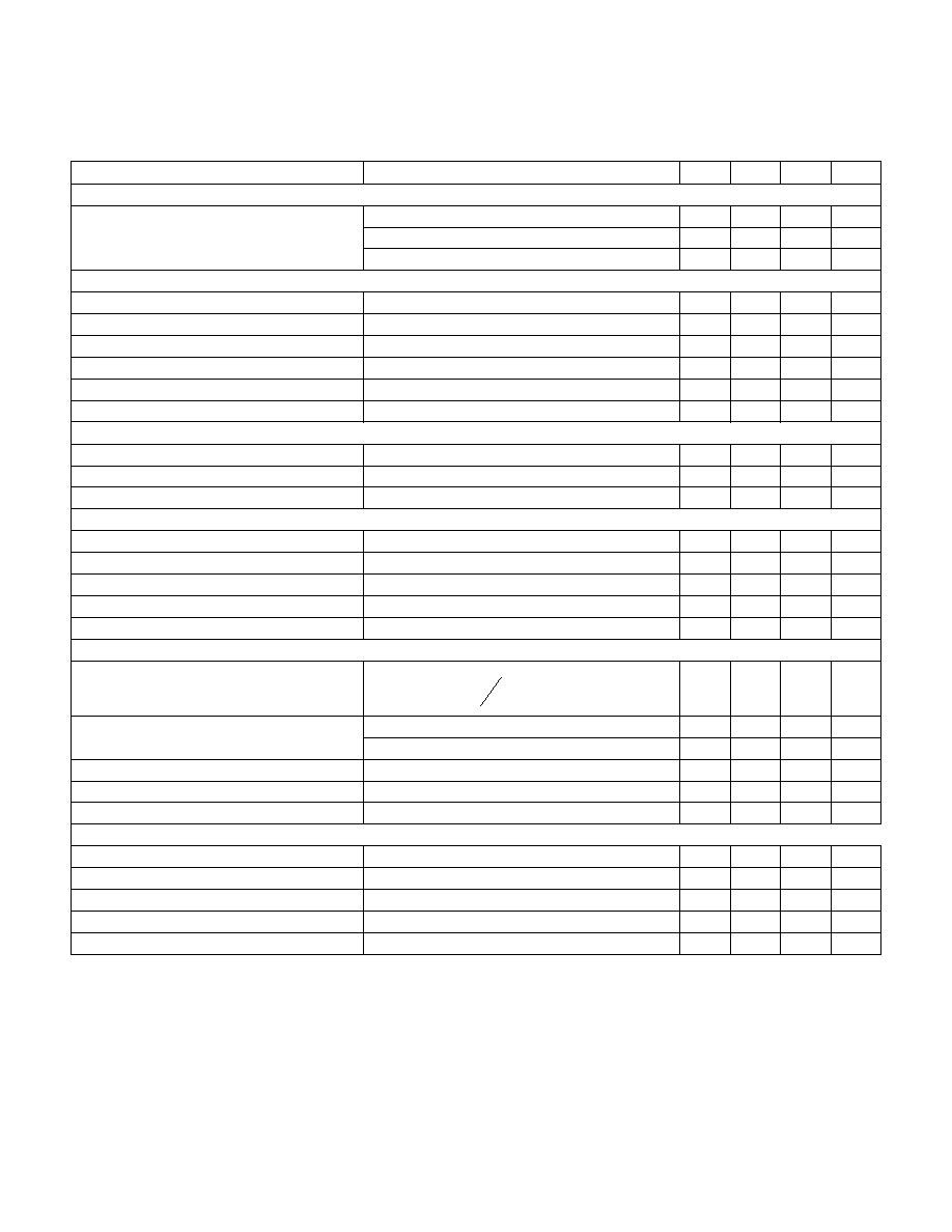
ELECTRICAL CHARACTERISTICS
Unless otherwise stated, these specifications apply for T
A
= T
J
= 0∞C to 70∞C,
TRMPWR = 2.7V to 5.25V.
PARAMETER
TEST CONDITIONS
MIN
TYP
MAX
UNITS
TRMPWR Supply Current Section
TRMPWR Supply Current
LVD SCSI Mode
23
35
mA
SE Mode
14
25
mA
DISCNCT Mode
250
500
µA
Regulator Section
1.25V Regulator Output Voltage
LVD SCSI Mode
1.15
1.25
1.35
V
1.25V Regulator Source Current
V
REG
= 0V
≠225
≠420
≠800
mA
1.25V Regulator Sink Current
V
REG
= 3.3V
100
180
420
mA
2.7V Regulator Output Voltage
SE Mode
2.5
2.7
3.0
V
2.7V Regulator Source Current
V
REG
= 0V
≠225
≠420
≠800
mA
2.7V Regulator Sink Current
V
REG
= 3.3V
100
180
420
mA
Diff Sense Driver (DIFSENS) Section
1.3V DIFSENS Output Voltage
DIFSENS
1.2
1.3
1.4
V
1.3V DIFSENS Source Current
V
DIFSENS
= 0V
≠5
≠15
mA
1.3V DIFSENS Sink Current
V
DIFSENS
= 2.75V
50
200
µA
Differential Termination Section
Differential Impedance
100
105
110
Common Mode Impedance
(Note 2)
110
150
165
Differential Bias Voltage
100
125
mV
Common Mode Bias
1.15
1.25
1.35
V
Output Capacitance
Single Ended Measurement to Ground (Note 1)
3
pF
Single Ended Termination Section
Impedance
Z
VL
V
IL
X
X
=
-
(
.
)
0 2
, (Note 3)
100
108
116
Termination Current
Signal Level 0.2V, All Lines Low
≠20
≠23
≠25.4
mA
Signal Level 0.5V
≠17
≠22.4
mA
Output Leakage
400
nA
Output Capacitance
Single Ended Measurement to Ground (Note 1)
3
pF
Single Ended GND SE Impedance
I= 10mA
20
60
Disconnect (DISCNCT) and Diff Buffer (DIFFB) Input Section
DISCNCT Threshold
0.8
2.0
V
DISCNCT Input Current
≠10
≠30
µA
DIFFB SE to LVD SCSI Threshold
0.5
0.7
V
DIFFB LVD SCSI to HPD Threshold
1.9
2.4
V
DIFFB Input Current
≠1
1
µA
4
UCC5672
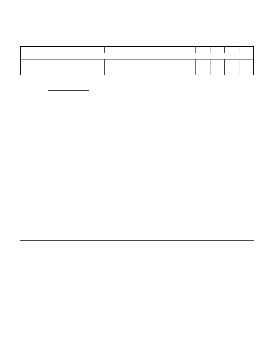
ELECTRICAL CHARACTERISTICS
Unless otherwise stated, these specifications apply for T
A
= T
J
= 0∞C to 70∞C,
TRMPWR = 2.7V to 5.25V.
PARAMETER
TEST CONDITIONS
MIN
TYP
MAX
UNITS
Time Delay/Filter Section
Mode Change Delay
A new mode change can start any time after a
previous mode change has been detected.
(Note4 )
100
180
300
ms
Note 1: Guaranteed by design. Not 100% tested in production.
Note 2:
(
) (
)
Z
V
I
I
CM
V
V
V
V
CM
CM
=
-
+
-
1 2
0 6
0 6
.
.
.
; Where VCM = Voltage measured with L+ tied to L≠ and zero current applied;
Note 3: VL
X
= Output voltage for each terminator minus output pin (L1≠ through L9≠) with each pin unloaded.
IL
X
= Output current for each terminator minus output pin (L1≠ through L9≠) with the minus output pin forced to 0.2V.
Note 4: Noise on DIFFB will not cause a false mode change. The time delay is that same for a change from any mode to any
other mode. Within 300ms after power is applied the mode is defined by the voltage of DIFFB.
PIN DESCRIPTIONS
DIFFB:
Input pin for the comparators that select SE,
LVD SCSI, or HIPD modes of operation. This pin should
be decoupled with a 0.1
µF capacitor to ground and then
coupled to the DIFSENS pin through a 20k
resistor.
DIFSENS: Connects to the Diff Sense line of the SCSI
bus. The bus mode is controlled by the voltage level on
this pin.
DISCNCT: Input pin used to shut down the terminator if
the terminator is not connected at the end of the bus.
Connect this pin to ground to activate the terminator or
open pin to disable the terminator.
HS/GND: Heat sink ground pins. These should be con-
nected to large ground area PC board traces to increase
the power dissipation capability.
GND: Power Supply return.
L1≠ thru L9≠: Termination lines. These are the active
lines in SE mode and are the negative lines for LVD
SCSI mode. In HIPD mode, these lines are high imped-
ance.
L1+ thru L9+: Termination lines. These lines switch to
ground in SE mode and are the positive lines for LVD
SCSI mode. In HIPD mode, these lines are high imped-
ance.
REG: Regulator bypass pin, must be connected to a
4.7
µF capacitor to ground.
TRMPWR: 2.7V to 5.25V power input pin. Bypass near
the terminators with a 4.7
µF capacitor to ground.
All SCSI buses require a termination network at each
end to function properly. Specific termination require-
ments differ, depending on which types of SCSI devices
are present on the bus.
The UCC5672 is used in multi-mode active termination
applications, where single ended (SE) and low voltage
differential (LVD) SCSI devices might coexist. The
UCC5672 has both SE and LVD SCSI termination net-
works integrated into a single monolithic component. The
correct termination network is automatically determined
by the SCSI bus "DIFSENS" signal.
The SCSI bus DIFSENS signal line is used to identify
which types of SCSI devices are present on the bus. On
power-up, the UCC5672 DIFSENS drivers will try to de-
liver 1.3V to the DIFSENS line. If only LVD SCSI devices
are present, the DIFSENS line will be successfully driven
to 1.3V and the terminators will configure for LVD SCSI
operation. If any single ended devices are present, they
will present a short to ground on the DIFSENS line, sig-
naling the UCC5672(s) to configure into the SE mode,
accommodating the SE devices. Or, if any high voltage
differential
(HVD)
SCSI
devices
are
present,
the
DIFSENS line is pulled high and the terminator will enter
a high impedance state, effectively disconnecting from
the bus.
The DIFSENS line is monitored by each terminator
through a 50Hz noise filter at the DIFFB input pin. A set
of comparators detect and select the appropriate termi-
APPLICATION INFORMATION
5
UCC5672
nation for the bus as follows. If the DIFSENS signal is
below 0.5V, the termination network is set for single
ended. Between 0.7V and 1.9V, the termination network
switches to LVD SCSI, and above 2.4V indicates HVD
SCSI, causing the terminators to disconnect from the
bus. These thresholds accommodate differences in
ground potential that can occur with long lines.
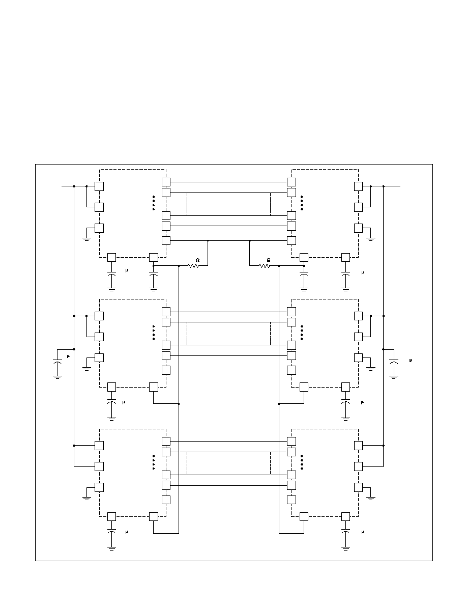
Three UCC5672 multi-mode parts are required at each
end of the bus to terminate 27 (18 data, plus 9 control)
lines. Each part includes a DIFSENS driver, but only one
is necessary to drive the line. The DIFFB inputs on all
three parts are connected together, allowing them to
share the same 50Hz noise filter. This multi-mode termi-
nator operates in full specification down to 2.7V
TRMPWR voltage. This accommodates 3.3V systems,
APPLICATION INFORMATION (cont.)
REG
DIFFB
16
1
17
16
CONTROL LINES (9)
20 k
20 k
DIFF SENSE
4
2
5
3
4.7 F
0.1
µF
31
25
32
26
L1+
L1≠
L9+
L9≠
L1+
L1≠
L9+
L9≠
DIFFS
UCC5672
UCC5672
DIFFS
REG
DIFFB
1
17
4.7 F
0.1
µF
REG
DIFFB
1
17
DATA LINES (9)
4
2
5
3
4.7 F
31
25
32
26
L1+
L1≠
L9+
L9≠
L1+
L1≠
L9+
L9≠
UCC5672
UCC5672
REG
DIFFB
1
17
4.7 F
REG
TRMPWR
DIFFB
28
1
17
DATA LINES (9)
2
2
3
3
4.7 F
25
25
26
26
L1+
L1≠
L9+
L9≠
L1+
L1≠
L9+
L9≠
UCC5672
UCC5672
27
TRMPWR
13
DISCNCT
REG
DIFFB
1
17
4.7 F
TRMPWR
28
27
TRMPWR
13
DISCNCT
TRMPWR
28
27
TRMPWR
13
DISCNCT
28
27
13
TRMPWR
TRMPWR
DISCNCT
28
27
13
TRMPWR
TRMPWR
DISCNCT
28
27
13
TRMPWR
TRMPWR
DISCNCT
16
NC
16
NC
NC
16
NC
16
4.7 F
4.7 F
Termpower
Termpower
Figure 1. Application diagram.
Note: Indicated pinout is for 28 pin TSSOP package.
UDG-99126

6
UCC5672
with allowance for the 3.3V supply tolerance (+/- 10%), a
unidirectional fusing device and cable drop. In 3.3V
TRMPWR systems, the UCC3918 is recommended in
place of the fuse and diode. The UCC3918's lower volt-
age drop allows additional margin over the fuse and di-
ode, for the far end terminator.
Layout is critical for Ultra2, Ultra3/Ultra160 and Ultra320
systems. The SPI-2 standard for capacitance loading is
10pF maximum from each positive and negative signal
line to ground, and a maximum of 5pF between the posi-
tive and negative signal lines of each pair is allowed.
These maximum capacitances apply to differential bus
termination circuitry that is not part of a SCSI device,
(e.g. a cable terminator). If the termination circuitry is in-
cluded as part of a SCSI device, (e.g., a host adaptor,
disk or tape drive), then the corresponding requirements
are 30pF maximum from each positive and negative sig-
nal line to ground and 15pF maximum between the posi-
tive and negative signal lines of each pair.
The SPI-2 standard for capacitance balance of each pair
and balance between pairs is more stringent. The stan-
dard is 0.75pF maximum difference from the positive and
negative signal lines of each pair to ground. An additional
requirement is a maximum difference of 2pF when com-
paring pair to pair. These requirements apply to differen-
tial bus termination circuitry that is not part of a SCSI
device. If the termination circuitry is included as part of a
device, then the corresponding balance requirements are
2.25pF maximum difference within a pair, and 3pF from
pair to pair.
Feed-throughs,
through-hole
connections,
and
etch
lengths
need
to
be
carefully
balanced.
Standard
multi-layer power and ground plane spacing add about
1pF to each plane. Each feed-through will add about
2.5pF to 3.5pF. Enlarging the clearance holes on both
power and ground planes will reduce the capacitance.
Similarly, opening up the power and ground planes under
the
connector
will
reduce
the
capacitance
for
through-hole connector applications. Capacitance
will
also be affected by components, in close proximity,
above and below the circuit board.
Unitrode multi-mode terminators are designed with very
tight balance, typically 0.1pF between pins in a pair and
0.3pF between pairs. At each L+ pin, a ground driver
drives the pin to ground, while in single ended mode. The
ground driver is specially designed to not effect the ca-
pacitive balance of the bus when the device is in LVD
SCSI or disconnect mode.
Multi-layer boards need to adhere to the 120
imped-
ance standard, including the connectors and feed-
throughs. This is normally done on the outer layers with
4 mil etch and 4 mil spacing between runs within a pair,
and a minimum of 8 mil spacing to the adjacent pairs to
reduce crosstalk. Microstrip technology is normally too
low of impedance and should not be used. It is designed
for 50
rather than 120 differential systems. Careful
consideration must be given to the issue of heat manage-
ment. A multi-mode terminator, operating in SE mode,
will dissipate as much as 130mW of instantaneous power
per active line with TRMPWR = 5.25V. The UCC5672 is
offered in a 28 pin TSSOP. This package includes two
heat sink ground pins. These heat sink/ground pins are
directly connected to the die mount paddle under the die
and conduct heat from the die to reduce the junction tem-
perature. Both of the HS/GND pins need to be connected
to etch area or four feed-through per pin connecting to
the ground plane layer on a multi-layer board.
APPLICATION INFORMATION (cont.)

IMPORTANT NOTICE
Texas Instruments Incorporated and its subsidiaries (TI) reserve the right to make corrections, modifications,
enhancements, improvements, and other changes to its products and services at any time and to discontinue
any product or service without notice. Customers should obtain the latest relevant information before placing
orders and should verify that such information is current and complete. All products are sold subject to TI's terms
and conditions of sale supplied at the time of order acknowledgment.
TI warrants performance of its hardware products to the specifications applicable at the time of sale in
accordance with TI's standard warranty. Testing and other quality control techniques are used to the extent TI
deems necessary to support this warranty. Except where mandated by government requirements, testing of all
parameters of each product is not necessarily performed.
TI assumes no liability for applications assistance or customer product design. Customers are responsible for
their products and applications using TI components. To minimize the risks associated with customer products
and applications, customers should provide adequate design and operating safeguards.
TI does not warrant or represent that any license, either express or implied, is granted under any TI patent right,
copyright, mask work right, or other TI intellectual property right relating to any combination, machine, or process
in which TI products or services are used. Information published by TI regarding third≠party products or services
does not constitute a license from TI to use such products or services or a warranty or endorsement thereof.
Use of such information may require a license from a third party under the patents or other intellectual property
of the third party, or a license from TI under the patents or other intellectual property of TI.
Reproduction of information in TI data books or data sheets is permissible only if reproduction is without
alteration and is accompanied by all associated warranties, conditions, limitations, and notices. Reproduction
of this information with alteration is an unfair and deceptive business practice. TI is not responsible or liable for
such altered documentation.
Resale of TI products or services with statements different from or beyond the parameters stated by TI for that
product or service voids all express and any implied warranties for the associated TI product or service and
is an unfair and deceptive business practice. TI is not responsible or liable for any such statements.
Mailing Address:
Texas Instruments
Post Office Box 655303
Dallas, Texas 75265
Copyright
2002, Texas Instruments Incorporated