UCC5681
9 LINE LVD ONLY SCSI TERMINATOR WITH INTEGRATED
SPI 3 DELAYS AND REVERSE DISCONNECT
SLUS441A ≠ MARCH 1999 ≠ REVISED AUGUST 2000
1
POST OFFICE BOX 655303
∑
DALLAS, TEXAS 75265
D
LVD-Only Active Termination
D
2.7 V to 5.25 V Operation
D
Differential Failsafe Bias
D
Built-In SPI-3 Mode Change Filter/Delay
D
Standards Supported: SPI-3, Ultra2
(Fast 40), Ultra3/Ultra160 (Fast 80)
D
Reversed Disconnect Polarity
description
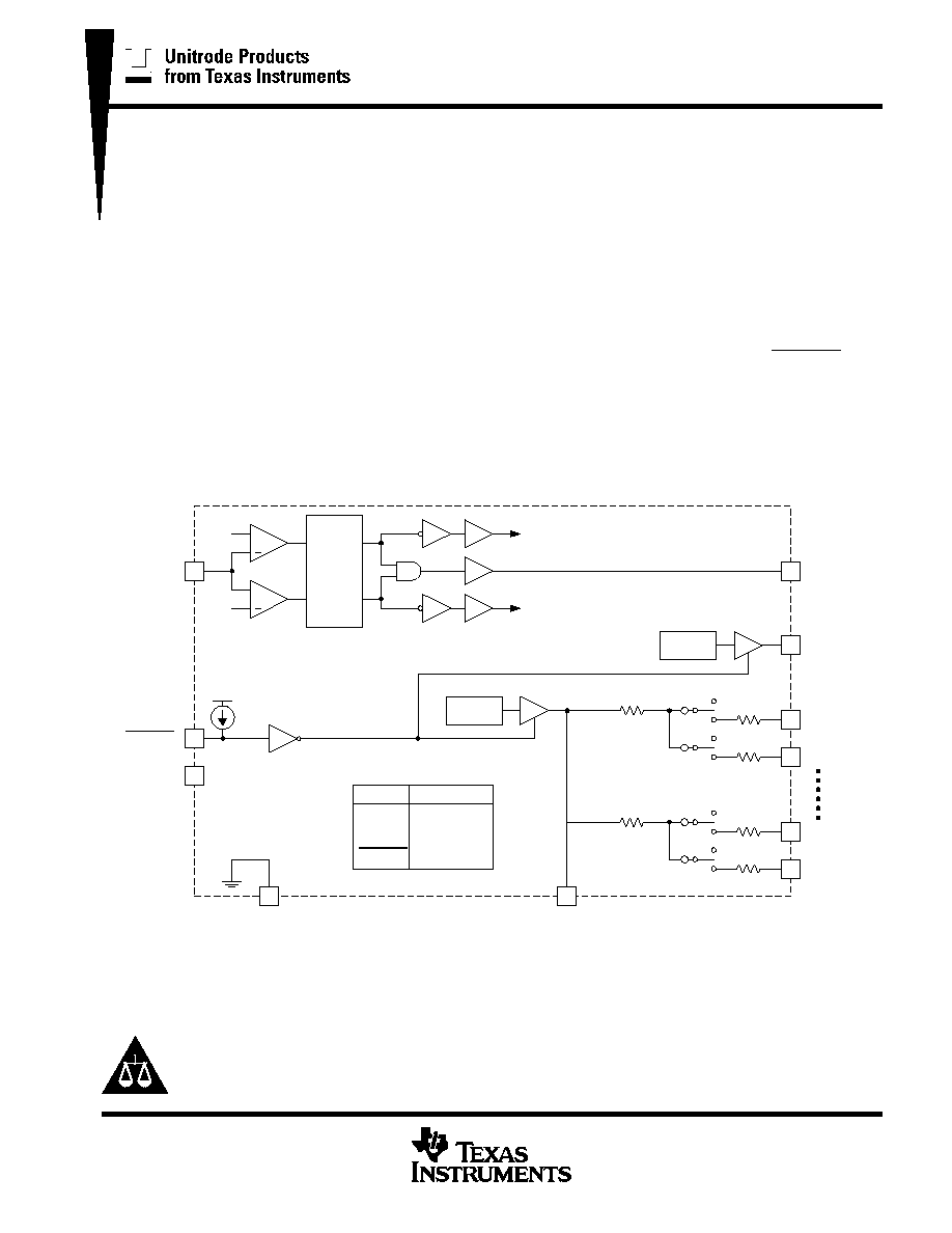
The UCC5681 is an LVD-only Small Computer System Interface (SCSI) terminator that integrates the mode
change delay function required by the SPI-3 specification. The device senses what types of SCSI drivers are
present on the bus via the voltage on the DIFFSENS SCSI control line. Single-ended (SE) and high-voltage
differential (HVD) SCSI drivers (EIA485) are not supported. If the chip detects the presence of an SE or HVD
SCSI driver, it disconnects itself by switching all terminating resistors off the bus and enters a high-impedance
state. The terminator can also be commanded to disconnect the terminating resistors with the DISCNCT input.
Impedance is trimmed for accuracy and maximum effectiveness. Bus lines are biased to a failsafe state to
ensure signal integrity.
The UCC5681 is offered in both 24-pin and 28-pin TSSOP (PW) packages for a temperature range of 0
∞
C to
70
∞
C.
functional block diagram
UDG≠00126
11
12
15
100 ms
TO
300 ms
DELAY/
FILTER
DIFFB
2.15 V
0.6 V
10
µ
A
HIGH≠VOLTAGE
DIFFERENTIAL
LOW≠VOLTAGE
DIFFERENTIAL
SINGLE≠ENDED
REF
1.3V
≠15 mA
I
SOURCE
≠5 mA
50
µ
A
I
SINK
200
µ
A
4
52
52
3
124
56 mV
56 mV
+ ≠
≠ +
25
26
L1 ≠
L1+
L9 ≠
L9+
REF
1.25V
1
REG
28
TRMPWR
14
GND
DIFSENS
52
52
124
56 mV
56 mV
+ ≠
≠ +
27
SE
LVD
HVD
DISCNCT
OPEN
DOWN
OPEN
OPEN
MODE
ALL SWITCHES
ENABLE
+
+
LVD
{
{
28-PIN PACKAGE ONLY
DISCNCT
DIS
DISCNCT
Copyright
2000, Texas Instruments Incorporated
PRODUCTION DATA information is current as of publication date.
Products conform to specifications per the terms of Texas Instruments
standard warranty. Production processing does not necessarily include
testing of all parameters.
Please be aware that an important notice concerning availability, standard warranty, and use in critical applications of
Texas Instruments semiconductor products and disclaimers thereto appears at the end of this data sheet.
UCC5681
9 LINE LVD ONLY SCSI TERMINATOR WITH INTEGRATED
SPI 3 DELAYS AND REVERSE DISCONNECT
SLUS441A ≠ MARCH 1999 ≠ REVISED AUGUST 2000
2
POST OFFICE BOX 655303
∑
DALLAS, TEXAS 75265
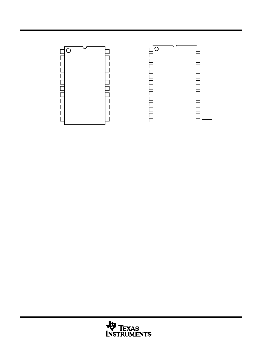
24-PIN PW PACKAGE
(TOP VIEW)
DIFFB
L6 ≠
L8+
L8 ≠
L7+
TRMPWR
L1+
N/C
L4 ≠
L3+
L4+
L1 ≠
L2+
L2 ≠
REG
L3 ≠
DIFSENS
L7 ≠
L6+
L5+
N/C
GND
14
13
12
11
10
9
8
7
6
5
4
3
2
1
15
16
17
18
19
20
21
22
23
24
25
26
27
28
L5 ≠
N/C
L9+
L9 ≠
LVD
DIFFB
L6 ≠
L8+
L8 ≠
L7+
TRMPWR
L1+
L4 ≠
L3+
L4+
L1 ≠
L2+
L2 ≠
REG
L3 ≠
DIFSENS
L7 ≠
L6+
L5+
L5 ≠
L9+
L9 ≠
GND
12
11
10
9
8
7
6
5
4
3
2
1
13
14
15
16
17
18
19
20
21
22
23
24
28-PIN PW PACKAGE
(TOP VIEW)
DISCNCT
DISCNCT
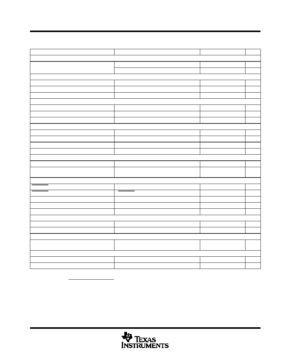
absolute maximum ratings over operating free-air temperature (unless otherwise noted)
TERMPWR Voltage
6 V
. . . . . . . . . . . . . . . . . . . . . . . . . . . . . . . . . . . . . . . . . . . . . . . . . . . . . . . . . . . . . . . . . . . . . . . . .
Signal Line Voltage
0 V to 5 V
. . . . . . . . . . . . . . . . . . . . . . . . . . . . . . . . . . . . . . . . . . . . . . . . . . . . . . . . . . . . . . . . . . . .
Package Dissipation
0.5 W
. . . . . . . . . . . . . . . . . . . . . . . . . . . . . . . . . . . . . . . . . . . . . . . . . . . . . . . . . . . . . . . . . . . . . . .
Storage Temperature
≠65
∞
C to 150
∞
C
. . . . . . . . . . . . . . . . . . . . . . . . . . . . . . . . . . . . . . . . . . . . . . . . . . . . . . . . . . . . .
Junction Temperature
≠55
∞
C to 150
∞
C
. . . . . . . . . . . . . . . . . . . . . . . . . . . . . . . . . . . . . . . . . . . . . . . . . . . . . . . . . . . .
Lead Temperature (Soldering, 10 sec.)
300
∞
C
. . . . . . . . . . . . . . . . . . . . . . . . . . . . . . . . . . . . . . . . . . . . . . . . . . . . .
Stresses beyond those listed under "absolute maximum ratings" may cause permanent damage to the device. These are stress ratings only, and
functional operation of the device at these or any other conditions beyond those indicated under "recommended operating conditions" is not
implied. Exposure to absolute-maximum-rated conditions for extended periods may affect device reliability.
recommended operating conditions
TERMPWR Voltage
2.7 V to 5.25 V
. . . . . . . . . . . . . . . . . . . . . . . . . . . . . . . . . . . . . . . . . . . . . . . . . . . . . . . . . . . . . . .
Operating Temperature Range
0
∞
C to 70
∞
C
. . . . . . . . . . . . . . . . . . . . . . . . . . . . . . . . . . . . . . . . . . . . . . . . . . . . . . . .
UCC5681
9 LINE LVD ONLY SCSI TERMINATOR WITH INTEGRATED
SPI 3 DELAYS AND REVERSE DISCONNECT
SLUS441A ≠ MARCH 1999 ≠ REVISED AUGUST 2000
3
POST OFFICE BOX 655303
∑
DALLAS, TEXAS 75265
electrical characteristics over recommended operating free-air temperature range,
T
A
= T
J
= 0
∞
C to 70
∞
C, TRMPWR = 2.7 V to 5.25 V
PARAMETER
TEST CONDITIONS
MIN
TYP
MAX
UNIT
TRMPWR Supply Current Section
TRMPWR s ppl c rrent
LVD Mode (No Load)
35
mA
TRMPWR supply current
Disabled Mode
500
µ
A
Regulator Section
Regulator output voltage
0.5 V
VCM
2.0, See Note 1
1.15
1.25
1.35
V
Regulator short-circuit source current
VREG = 0 V
-100
-80
mA
Regulator short-circuit sink current
VREG = 3.0 V
80
100
mA
DIFSENS Output Section
Output voltage
≠5 mA
IDIFSENS
50
µ
A
1.2
1.3
1.4
V
Short-circuit source current
VDIFSENS = 0 V
-15
-5
mA
Short-circuit sink current
VDIFSENS = 2.75 V
50
200
µ
A
Differential Termination Section (Applies to each line pair , 1-9, in LVD mode)
Differential impedance
100
105
110
Common-mode impedance
L+ and L- shorted together,
See Note 2
110
150
165
Differential bias voltage
100
125
mV
Common-mode bias voltage
L+ and L- shorted together
1.15
1.25
1.35
V
Disconnected Termination Section (Applies to each line pair , 1-9, in DISCNCT, SE or HVD mode)
Output leakage
400
nA
Output capacitance
Single-ended measurement to ground,
See Note 3
3
pF
DISCNCT and DIFFB Input Section
DISCNCT threshold
0.8
2.0
V
DISCNCT input current
VDISCNCT = 0 V and 2.0 V
-30
-10
µ
A
DIFFB SE to LVD threshold
0.5
0.7
V
DIFFB LVD to HVD threshold
1.9
2.4
V
DIFFB input current
0 V
VDIFFB
2.75 V
-10
10
µ
A
Low Voltage Differential (LVD) Status Bit Section (See Note 4)
ISOURCE
VLOAD = 2.4 V
-6
-4
mA
ISINK
VLOAD = 0.4 V
2
5
mA
Time Delay/Filter Section
Mode change delay
A new mode change can start any time after a
previous mode change has been detected
100
190
300
ms
Thermal Shutdown Section
Themal shutdown threshold
For increasing temperature
140
155
170
∞
C
Themal shutdown hysteresis
10
∞
C
NOTES:
1. VCM is applied to all L+ and L- lines simultaneously.
2. Z
CM
+
(2.0V
*
0.5V)
I
VCM(max)
*
I
VCM(min)
@ V
CM(max)
= 2.0, V
CM(min)
= 0.5 V
3. Ensured by design, not production tested.
4. This applies to the 28-pin package only.
UCC5681
9 LINE LVD ONLY SCSI TERMINATOR WITH INTEGRATED
SPI 3 DELAYS AND REVERSE DISCONNECT
SLUS441A ≠ MARCH 1999 ≠ REVISED AUGUST 2000
4
POST OFFICE BOX 655303
∑
DALLAS, TEXAS 75265
pin descriptions
DIFFB: DIFFSENS input pin. Connect through a 20-k
resistor to DIFSENS and through a 0.1-
µ
F capacitor
to ground. Input to comparators that detect what types of drivers are connected to the SCSI bus.
DIFSENS: SCSI bus DIFSENS line driver.
DISCNCT: Disconnect pin. Shuts down the terminator (switches terminating resistors off the bus) when tied to
GND. The disconnect pin high (or OPEN) enables the terminator.
GND: Power supply return.
LINEn-: Line termination pins. Negative line in differential pair.
LINEn+: Line termination pins. Positive line in differential pair.
LVD: (28-pin package only) Indicates that the bus is in LVD mode.
REG: Regulator bypass pin. Bypass near the terminator with a 4.7-
µ
F and a high-frequency, low-ESR 0.01-
µ
F
capacitor to ground.
TRMPWR: V
IN
2.75 V to 5.25 V supply. Bypass near the terminator with a 4.7-
µ
F and a high-frequency, low-ESR
0.01-
µ
F capacitor to ground.
APPLICATION INFORMATION
All SCSI buses require a termination network at each end to function properly. Specific termination requirements
differ, depending on which types of SCSI driver devices are present on the bus. The UCC5681 is a low-voltage
differential (LVD)-only device. It senses which types of drivers are present on the bus. If it detects the presence
of a single-ended (SE) or high-voltage differential (HVD) driver, the UCC5681 will place itself in a
high-impedance input state, effectively disconnecting the chip from the bus.
The UCC5681 senses what kinds of drivers are present on the bus by the voltage on SCSI bus control line
DIFFSENS, which is monitored by the DIFFB input pin. The DIFSENS output pin on the UCC5681 attempts to
drive a DIFFSENS control line to 1.3 V. If only LVD devices are present, the DIFFSENS line will be successfully
driven to that voltage. If HVD drivers are present, they will pull the DIFFSENS line high. If any single-ended
drivers are present, they pull the DIFSENS line to ground (even if HVD drivers are also present on the bus). If
the voltage on the DIFFB is below 0.5 V or above 2.4 V, the UCC5681 enters the high-impedance SE/HVD state.
If it is between 0.7 V and 1.9 V, the UCC5681 enters the LVD mode. These thresholds accommodate differences
in ground potential that can occur between the ends of long bus lines.
Three UCC5681 ICs are required at each end of the SCSI bus to terminate 27 lines (18 data, 9 control). Every
UCC5681 contains a DIFSENS driver, but only one should be used to drive the line at each end. The DIFSENS
pin on the other devices should be left unconnected.
On power up (the voltage on the TRMPWR pin rising above 2.7 V), the UCC5681 assumes the SE/HVD mode.
If the voltage on the DIFFB input indicates LVD mode, the chip waits 100 ms to 300 ms before changing the
mode of the bus. If the voltage at the DIFFB input later crosses one of the thresholds, the UCC5681 again waits
100 ms to 300 ms before changing the mode of the bus. The magnitude of the delay is the same when changing
in or out of either bus mode. A new mode change can start anytime after a previous mode change has been
detected.
The DIFFB inputs on all three chips at each end of the bus should be connected together. Properly filtered, noise
on DIFFB will not cause a false mode change. There should be a shared 50-Hz noise filter implemented on
DIFFB at each end of the bus as close as possible to the DIFFB pins. This is implemented with a 20-k
resistor
between the DIFFB and DIFSENS pins, and a 0.1-
µ
F capacitor from DIFFB to ground. See the Typical
Application diagram at the end of this datasheet.
UCC5681
9 LINE LVD ONLY SCSI TERMINATOR WITH INTEGRATED
SPI 3 DELAYS AND REVERSE DISCONNECT
SLUS441A ≠ MARCH 1999 ≠ REVISED AUGUST 2000
5
POST OFFICE BOX 655303
∑
DALLAS, TEXAS 75265
APPLICATION INFORMATION (continued)
In LVD mode, the regulated voltage is switched to 1.25 V and a resistor network is presented to each line pair
that provides common-mode impedance of 150
and differential impedance of 105
. The lines in each
differential pair are biased so that when not driven, Line(n)+ and Line(n)≠ are driven 56 mV below and above
the common-mode bias voltage (1.25 V) respectively.
In SE/HVD mode, all the terminating resistors are switched off the bus. The 1.25-V and 1.3-V (DIFSENS)
regulators are left on.
When the disconnect input (DISCNCT) is low, the terminating resistors are switched off the bus and both voltage
regulators are turned off to save power. The mode change filter/delay function is still active and the LVD pin (in
the 28-pin package) continues to indicate the correct bus mode.
The UCC5681 operates down to a TRMPWR voltage of 2.7 V. This accommodates a 3.3-V system with
allowance for supply tolerance (
±
10%), a unidirectional fusing device, and cable drop. The UCC3916 is
recommended in place of a fuse and diode implementation, as its lower voltage drop provides additional voltage
margin for the system.
Layout is important in all SCSI implementations and critical in SPI-3 systems, which have stringent requirements
on both the absolute value of capacitance on differential signal lines and the balancing of capacitance between
paired lines and from pair to pair.
Feedthroughs, through-hole connections, and etch lengths need to be carefully balanced. Standard multilayer
power and ground plane spacing adds about 1 pF to each plane. Each feed-through will add 2.5 pF to 3.5 pF.
Enlarging the clearance holes on both power and ground planes reduces capacitance. Opening up the power
and ground planes under a through-hole connector reduces added capacitance in those applications.
Capacitance is also affected by components in close proximity on both sides of the board.
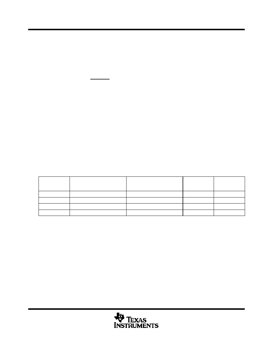
maximum capacitance
SCSI Class
Trace to GND:
REQ, ACK, DATA, Parity,
P_CRCA
Trace to Trace:
REQ, ACK, DATA, Parity,
P_CRCA
Trace to GND:
Other signals
Trace to Trace:
Other Signals
Ultra1
25 pF
N/A
25 pF
N/A
Ultra2
20 pF
10 pF
25 pF
13 pF
Ultra3/Ultra160
15 pF
8 pF
25 pF
13 pF
Ultra320
13 pF
6.5 pF
21 pF (est.)
10 pF (est.)
TI terminators are designed with very tightly controlled capacitance on their signal lines. Between the positive
and negative lines in a differential pair the difference is typically no more than 0.1 pF, and only 0.3 pF between
pairs.
Multi-layer boards need to adhere to the 120-
impedance standard, including the connector and feedthroughs.
Bus traces are normally run on the outer layers of the board with 4-mil etch and 4-mil spacing between the two
lines in each differential pair, and a minimum of 8-mil spacing to adjacent pairs to minimize crosstalk. Microstrip
technology is too low in impedance and should not be used--it is designed for 50
rather than 120-
differential
systems.
Decoupling capacitors should be installed as close as possible to the following input pins of the UCC5681:
TRMPWR: 4.7-
µ
F capacitor to ground, 0.01-
µ
F capacitor to ground (high-frequency, low ESR)
REG: 4.7-
µ
F capacitor to ground, 0.01-
µ
F capacitor to ground (high-frequency, low ESR)

UCC5681
9 LINE LVD ONLY SCSI TERMINATOR WITH INTEGRATED
SPI 3 DELAYS AND REVERSE DISCONNECT
SLUS441A ≠ MARCH 1999 ≠ REVISED AUGUST 2000
6
POST OFFICE BOX 655303
∑
DALLAS, TEXAS 75265
TYPICAL APPLICATION
UDG-00125
REG
TRMPWR
TRMPWR
DIFFB
REG
TERMPWR
TERMPWR
28
15
12
1
11
11
1
24
13
CONTROL LINES (9)
20k
20k
(DIFFSENS)
3
2
4
3
4.7
µ
F
0.1
µ
F
25
26
23
22
L1+
L1≠
L9+
L9≠
L1+
L1≠
L9+
L9≠
DIFFB
10
0.1
µ
F
TRMPWR
TRMPWR
DIFFB
REG
28
15
11
1
24
13
DATA LINES (9)
3
2
4
3
26
23
25
22
L1+
L1≠
L9+
L9≠
L1+
L1≠
L9+
L9≠
DIFFB
10
TRMPWR
TRMPWR
DIFFB
28
15
11
24
13
DATA LINES (9)
3
2
4
3
26
23
25
22
L1+
L1≠
L9+
L9≠
L1+
L1≠
L9+
L9≠
DIFFB
10
0.01
µ
F
27
LVD
S2*
SCSI CONTROLLER
DIFFSENS INPUT
DIFSENS
0.01
µ
F
4.7
µ
F
0.01
µ
F
4.7
µ
F
0.01
µ
F
REG
1
4.7
µ
F
0.01
µ
F
REG
1
4.7
µ
F
0.01
µ
F
REG
1
4.7
µ
F
0.01
µ
F
4.7
µ
F
0.01
µ
F
4.7
µ
F
12
11
12
11
DIFSENS
DIFSENS
DIFSENS
DIFSENS
DIFSENS
N/C
N/C
N/C
N/C
S1
{
{
CLOSE S1 and S2 TO DISCONNECTTERMINATORS
UCC5681PW28
UCC5681PW28
UCC5681PW28
UCC5681PW24
UCC5681PW24
UCC5681PW24
DISCNCT
DISCNCT
DISCNCT
DISCNCT
DISCNCT
DISCNCT

IMPORTANT NOTICE
Texas Instruments and its subsidiaries (TI) reserve the right to make changes to their products or to discontinue
any product or service without notice, and advise customers to obtain the latest version of relevant information
to verify, before placing orders, that information being relied on is current and complete. All products are sold
subject to the terms and conditions of sale supplied at the time of order acknowledgment, including those
pertaining to warranty, patent infringement, and limitation of liability.
TI warrants performance of its products to the specifications applicable at the time of sale in accordance with
TI's standard warranty. Testing and other quality control techniques are utilized to the extent TI deems necessary
to support this warranty. Specific testing of all parameters of each device is not necessarily performed, except
those mandated by government requirements.
Customers are responsible for their applications using TI components.
In order to minimize risks associated with the customer's applications, adequate design and operating
safeguards must be provided by the customer to minimize inherent or procedural hazards.
TI assumes no liability for applications assistance or customer product design. TI does not warrant or represent
that any license, either express or implied, is granted under any patent right, copyright, mask work right, or other
intellectual property right of TI covering or relating to any combination, machine, or process in which such
products or services might be or are used. TI's publication of information regarding any third party's products
or services does not constitute TI's approval, license, warranty or endorsement thereof.
Reproduction of information in TI data books or data sheets is permissible only if reproduction is without
alteration and is accompanied by all associated warranties, conditions, limitations and notices. Representation
or reproduction of this information with alteration voids all warranties provided for an associated TI product or
service, is an unfair and deceptive business practice, and TI is not responsible nor liable for any such use.
Resale of TI's products or services with
statements different from or beyond the parameters stated by TI for
that product or service voids all express and any implied warranties for the associated TI product or service,
is an unfair and deceptive business practice, and TI is not responsible nor liable for any such use.
Also see: Standard Terms and Conditions of Sale for Semiconductor Products. www.ti.com/sc/docs/stdterms.htm
Mailing Address:
Texas Instruments
Post Office Box 655303
Dallas, Texas 75265
Copyright
2001, Texas Instruments Incorporated