
www.ti.com
FEATURES
APPLICATIONS
DESCRIPTION
UCD8220, UCD8620
SLUS652B ≠ MARCH 2005 ≠ REVISED SEPTEMBER 2005
DIGITALLY MANAGED PUSH-PULL ANALOG PWM CONTROLLERS
∑
10-ns Typical Rise and Fall Times with 2.2-nF
∑
For Digitally Managed Power Supplies Using
∑
25-ns Input-to-Output Propagation Delay
µ
Cs or the TMS320 TM DSP Family
∑
25-ns Current Sense-to-Output Propagation
∑
Voltage or Peak Current Mode Control with
Delay
Cycle-by-Cycle Current Limiting
∑
Programmable Current Limit Threshold
∑
Clock input from Digital Controller to set
∑
Digital Output Current Limit Flag
Operating Frequency and Max Duty Cycle
∑
4.5-V to 15.5-V Supply Voltage Range
∑
Analog PWM Comparator
∑
Rated from -40∞C to 105∞C
∑
2-MHz Switching Frequency
∑
110-V Input Startup Circuit and Thermal
Shutdown (UCD8620)
∑
Digitally Managed Switch Mode Power
∑
Internal Programmable Slope Compensation
Supplies
∑
3.3-V, 10-mA Linear Regulator
∑
Push-Pull, Half-Bridge, or Full-Bridge
Converters
∑
DSP/
µ
C Compatible Inputs
∑
Battery Chargers
∑
Dual ±4-A TrueDriveTM High Current Drivers
The UCD8220 and UCD8620 are members of the UCD8K family of analog pulse-width modulator devices to be
used in digitally managed power supplies using a microcontroller or the TMS320TM DSP family.
UCD8220 and UCD8620 are double-ended PWM controllers configured with push-pull drive logic. The UCD8620
has a 110-V high-voltage startup circuit which can directly start up the controller from a 48-V telecom input line.
Systems using UCD8K devices close the PWM feedback loop with traditional analog methods, but the UCD8K
controllers include circuitry to interpret a time-domain digital pulse train. The pulse train contains the operating
frequency and maximum duty cycle limit which are used to control the power supply operation. This eases
implementation of a converter with high level control features without the added complexity or possible PWM
resolution limitations of closing the control loop in the discrete time domain.
Figure 1. UCD8220 Typical Simplified Push-Pull Converter Application Schematic
Please be aware that an important notice concerning availability, standard warranty, and use in critical applications of Texas
Instruments semiconductor products and disclaimers thereto appears at the end of this data sheet.
TMS320, TrueDrive, PowerPAD are trademarks of Texas Instruments.
UNLESS OTHERWISE NOTED this document contains PRO-
Copyright © 2005, Texas Instruments Incorporated
DUCTION DATA information current as of publication date. Prod-
ucts conform to specifications per the terms of Texas Instruments
standard warranty. Production processing does not necessarily
include testing of all parameters.
www.ti.com
DESCRIPTION (continued)
SIMPLIFIED APPLICATION DIAGRAMS
UCD8220, UCD8620
SLUS652B ≠ MARCH 2005 ≠ REVISED SEPTEMBER 2005
The UCD8220 and UCD8620 can be configured for either peak current mode or voltage mode control. They
provide a programmable current limit function and a digital output current limit flag which can be monitored by the
host controller to set the current limit operation. For fast switching speeds, the output stages use the TrueDriveTM
architecture, which delivers rated current of ±4 A into the gate of a MOSFET. Finally they also include a 3.3-V,
10-mA linear regulator to provide power to the digital controller or act as a reference in the system.
The UCD8K controller family is compatible with the standard 3.3-V I/O ports of UCD9K digital power controllers,
DSPs, Microcontrollers, or ASICs and is offered in PowerPADTM HTSSOP and QFN packages.
Figure 2. UCD8220 Typical Simplified Half-Bridge Converter Application Schematic
2
www.ti.com
UCD8220, UCD8620
SLUS652B ≠ MARCH 2005 ≠ REVISED SEPTEMBER 2005
SIMPLIFIED APPLICATION DIAGRAMS (continued)
Figure 3. UCD8620 Typical Simplified Push-Pull Converter Application Schematic
Figure 4. UCD8620 Typical Simplified Half-Bridge Converter Application Schematic
3

www.ti.com
CONNECTION DIAGRAMS
1
2
3
4
5
6
7
8
16
15
14
13
12
11
10
9
HTSSOP PACKAGE (PWP -16)
UCD8620 (TOP VIEW)
NC - No internal connection
NC
CLK
3V3
ISET
AGND
CTRL
CLF
ILIM
VIN
NC
VDD
PVDD
OUT1
OUT2
PGND
CS
1
2
3
4
5
6
7
8
16
15
14
13
12
11
10
9
HTSSOP PACKAGE (PWP -16)
UCD8220 (TOP VIEW)
NC - No internal connection
NC
CLK
3V3
ISET
AGND
CTRL
CLF
ILIM
NC
NC
VDD
PVDD
OUT1
OUT2
PGND
CS
3V3
ISET
AGND
CTRL
CLF
NC
ILIM
NC
CS
NC
VDD
PVDD
OUT1
OUT2
PGND
QFN PACKAGE (RGW-20)
UCD8620 (BOTTOM VIEW)
20
19
18
17
16
6
7
8
9
10
CLK
NC
NC
VIN
NC
15 14 13 12 11
1
2
3
4
5
3V3
ISET
AGND
CTRL
16
15
14
13
CLK
NC
NC
VDD
QFN PACKAGE (RSA-16)
UCD8220 (BOTTOM VIEW)
5
6
7
8
1
CLF
ILIM
NC
CS
2
3
4
12
11
10
9
PVDD
OUT1
OUT2
PGND
UCD8220, UCD8620
SLUS652B ≠ MARCH 2005 ≠ REVISED SEPTEMBER 2005
These devices have limited built-in ESD protection. The leads should be shorted together or the device
placed in conductive foam during storage or handling to prevent electrostatic damage to the MOS gates.
ORDERING INFORMATION
PACKAGED DEVICES
(1) (2) (3)
110-V HV STARTUP
TEMPERATURE RANGE
PowerPADTM
CIRCUIT
QFN-16 (RSA)
(4)
QFN-20 (RGW)
HTSSOP-16 (PWP)
-40∞C to 105∞C
No
UCD8220PWP
UCD8220RSA
-
Yes
UCD8620PWP
(5)
-
UCD8620RGW
(1)
HTSSOP-16 (PWP), QFN-16 (RSA), and QFN-20 (RGW) packages are available taped and reeled. Add R suffix to device type (e.g.
UCD8620PWPR) to order quantities of 2,000 devices per reel for the PWP package and 1,000 devices per reel for the RSA and RGW
packages.
(2)
These products are packaged in Pb-Free and Green lead finish of Pd-Ni-Au which is compatible with MSL level 1 at 255∞C to 260∞C
peak reflow temperature to be compatible with either lead free or Sn/Pb soldering operations.
(3)
For the most current package and ordering information, see the Package Option Addendum at the end of this document, or see the TI
Web site at
www.ti.com
.
(4)
Contact factory for availability of QFN packaging.
(5)
Product preview stage of development.
4
www.ti.com
ABSOLUTE MAXIMUM RATINGS
(1) (2)
UCD8220, UCD8620
SLUS652B ≠ MARCH 2005 ≠ REVISED SEPTEMBER 2005
PACKAGING INFORMATION
POWER RATING T
A
RATING FACTOR
PACKAGE
SUFFIX
JC
(
∞
C/W)
JA
(
∞
C/W)
= 70
∞
C, T
J
= 125
∞
C
ABOVE 70
∞
C
(mW)
(mW/
∞
C)
PowerPadTM
PWP
2.07
37.47
(1)
1470
27
MSSOP-16
QFN-16
RSA
-
-
-
-
QFN-20
RGW
-
-
-
-
(1)
PowerPadTM soldered to the PWB with TI recommended PWB as defined in TI's Application Report ( TI Literature Number
SLMA002
)
with OLFM.
SYMBOL
PARAMETER
UCD8x20
UNIT
V
I
Input Line Voltage
UCD8620 only
110
V
V
DD
Supply Voltage
16
Quiescent
20
I
DD
Supply Current
mA
Switching, T
A
= 25
∞
C, T
J
= 125
∞
C, V
DD
= 12 V
200
V
O
Output Gate Drive Voltage
OUT
-1 to PVDD
V
I
O(sink)
4.0
Output Gate Drive Current
OUT
A
I
O(source)
-4.0
Analog Input
ISET, CS, CTRL, ILIM
-0.3 to 3.6
V
Digital I/O's
CLK, CLF
-0.3 to 3.6
T
A
= 25∞C (PWP-16 package)
2.67
W
Power Dissipation
T
A
= 25∞C (QFN-16 package)
-
T
A
= 25∞C (QFN-20 package)
-
UCD8220
-55 to 150
Junction Operating
T
J
Temperature
UCD8620
-55 to 130
∞C
T
stg
Storage Temperature
-65 to 150
HBM
Human body model
2000
ESD Rating
(3)
V
CDM
Change device model
500
Lead Temperature (Soldering, 10 sec)
300
∞C
(1)
Stresses beyond those listed under "absolute maximum ratings" may cause permanent damage to the device. These are stress ratings
only, and functional operation of the device at these or any other conditions beyond those indicated under "recommended operating
conditions" is not implied. Exposure to absolute-maximum-rated conditions for extended periods may affect device reliability.
(2)
All voltages are with respect to GND. Currents are positive into, negative out of the specified terminal.
(3)
Tested to JEDEC standard EIA/JESD22 - A114-B.
5

www.ti.com
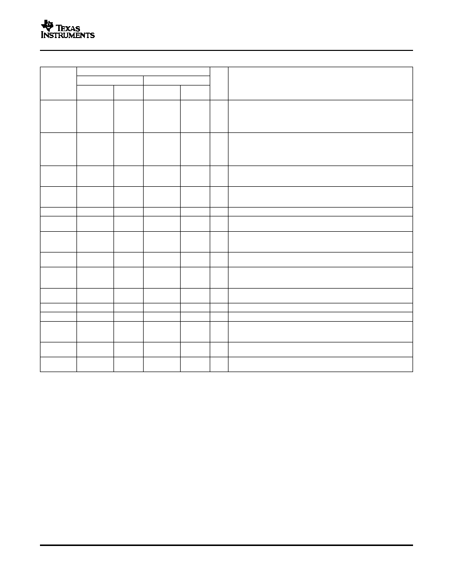
ELECTRICAL CHARACTERISTICS
UCD8220, UCD8620
SLUS652B ≠ MARCH 2005 ≠ REVISED SEPTEMBER 2005
V
DD
= 12 V, 4.7-µF capacitor from V
DD
to AGND, 1
µ
F from PVDD to PGND, 0.22-µF capacitor from 3V3 to AGND,
T
A
= T
J
= -40∞C to 105∞C, (unless otherwise noted).
PARAMETER
TEST CONDITIONS
MIN
TYP
MAX
UNIT
SUPPLY SECTION
UCD8620
500
800
Supply current, OFF
V
DD
= 4.2 V
µA
UCD8220
300
500
(UCD8620), outputs not switching, CLK = low
2
3
Supply current, ON
mA
(UCD8220), outputs not switching, CLK = low
2
3
LOW VOLTAGE UNDERVOLTAGE LOCKOUT (UCD8220 only)
V
DD
UVLO ON
4.25
4.5
4.75
V
V
DD
UVLO OFF
4.05
4.25
4.45
V
DD
UVLO hysteresis
150
250
350
mV
110-V HIGH VOLTAGE UNDERVOLTAGE LOCKOUT AND JFET CONTROL (UCD8620 ONLY)
V
DD
UVLO ON
12.5
13
13.5
V
DD
UVLO OFF
7
7.5
8
JFET turn-off threshold (V
START_JFET
) No switching, JFET on at startup
12.5
13
13.5
V
JFET turn-on threshold
No switching
11.5
12
12.5
JFET on/off hysteresis
1
V
DD
< 5 V, VIN = 18 V to 76 V
3
5
8
High voltage JFET current
mA
V
DD
= 12 V, VIN = 18 V to 76 V
10
Thermal shutdown, OFF
(1)
V
DD
= 5 V to 12 V
130
145
160
∞C
Thermal shutdown, ON
(1)
V
DD
> 5 V
110
125
140
REFERENCE / EXTERNAL BIAS SUPPLY
3V3 initial set point
T
A
= 25∞C, I
LOAD
= 0
3.267
3.3
3.333
V
3V3 set point over temperature
3.234
3.3
3.366
3V3 load regulation
I
LOAD
= 1 mA to 10 mA, VDD = 5 V
-
1
6.6
mV
3V3 line regulation
VDD = 4.75 V to 12 V, I
LOAD
= 10 mA
-
1
6.6
Short circuit current
VDD = 4.75 to 12 V
11
20
35
mA
3V3 OK threshold, ON
3.3 V rising
2.9
3.0
3.1
V
3V3 OK threshold, OFF
3.3 V falling
2.7
2.8
2.9
CLOCK INPUT (CLK)
HIGH, positive-going input threshold
1.65
-
2.08
voltage (VIT+)
LOW negative-going input threshold
1.16
-
1.5
V
voltage (VIT-)
Input voltage hysteresis,
0.6
-
0.8
(VIT+ - VIT-)
Frequency
OUTx = 1 MHz
-
-
2
MHz
Minimum allowable off time
(1)
20
ns
SLOPE COMPENSATION (ISET)
ISET Voltage
V
ISET
, 3V3 = 3.3 V, +/-2%
1.78
1.84
1.90
V
R
ISET
= 6.19 k
to AGND, CS = 0.25 V, CTRL = 2.5 V
1.48
2.12
2.76
m, V
SLOPE
(I-Mode)
R
ISET
= 100 k
to AGND, CS = 0.25 V, CTRL = 2.5 V
0.099
0.142
0.185
R
ISET
= 499 k
to AGND, CS = 0.25 V, CTRL = 2.5 V
0.019
0.028
0.037
V/µs
R
ISET
= 4.99 k
to 3V3, CTRL = 2.5 V
1.44
2.06
2.68
m, V
SLOPE
(V-Mode)
R
ISET
= 100 k
to 3V3, CTRL = 2.5 V
0.079
0.114
0.148
R
ISET
= 402 k
to 3v3, CTRL = 2.5 V
0.019
0.027
0.035
(1)
Ensured by design. Not 100% tested in production.
6

www.ti.com
VIT!
10%
90%
INPUT
OUTPUT
VIT+
t
D1
t
F
t
F
t
D2
UCD8220, UCD8620
SLUS652B ≠ MARCH 2005 ≠ REVISED SEPTEMBER 2005
ELECTRICAL CHARACTERISTICS (continued)
V
DD
= 12 V, 4.7-µF capacitor from V
DD
to AGND, 1
µ
F from PVDD to PGND, 0.22-µF capacitor from 3V3 to AGND,
T
A
= T
J
= -40∞C to 105∞C, (unless otherwise noted).
PARAMETER
TEST CONDITIONS
MIN
TYP
MAX
UNIT
ISET resistor range
Current mode control; R
ISET
connected to AGND
6.19
499
k
ISET resistor range
Voltage mode control; R
ISET
connected to 3V3
4.99
402
Voltage mode control with Feed-Forward; R
ISET
connected to
ISET current range
3.7
300
µ
A
VIN
PWM
PWM offset at CTRL input
3V3 = 3.3 V +/-2%
0.45
0.51
0.6
V
CTRL buffer gain
(1)
Gain from CTRL to PWM comparator input
0.5
V/V
CURRENT LIMIT (ILIM)
ILIM internal current limit threshold
ILIM = OPEN
0.466
0.5
0.536
V
ILIM maximum current limit threshold
ILIM = 3.3 V
0.975
1.025
1.075
V
ILIM current limit threshold
ILIM = 0.75 V
0.700
0.725
0.750
ILIM minimum current limit threshold
ILIM = 0.25 V
0.21
0.23
0.25
V
CLF output high level
CS > ILIM , I
LOAD
= -7 mA
2.64
-
-
V
CLF output low level
CS
ILIM, I
LOAD
= 7 mA
-
-
0.66
Propagation delay from CLK to CLF
CLK rising to CLF falling after a current limit event
-
15
25
ns
CURRENT SENSE COMPARATOR
Bias voltage
Includes CS comp offset
5
25
50
mV
Input bias current
-
≠1
-
µ
A
Propagation delay from CS to OUTx
ILIM = 0.5 V, measured on OUTx, CS = threshold + 60 mV
-
25
40
ns
Propagation delay from CS to CLF
ILIM = 0.5 V, measured on CLF, CS = threshold + 60 mV
-
25
50
CURRENT SENSE DISCHARGE TRANSISTOR
Discharge resistance
CLK = low, resistance from CS to AGND
10
35
75
OUTPUT DRIVERS
Source current
(2)
V
DD
= 12 V, CLK = high, OUTx = 5 V
-
4
-
Sink current
(2)
V
DD
= 12 V, CLK = low, OUTx = 5 V
-
4
-
A
Source current
(2)
V
DD
= 4.75 V, CLK = high, OUTx = 0
-
2
-
Sink current
(2)
V
DD
= 4.75 V, CLK = low, OUTx = 4.75 V
-
3
-
Rise time, t
R
C
LOAD
= 2.2 nF, V
DD
= 12 V
-
10
20
ns
Fall time, t
F
C
LOAD
= 2.2 nF, V
DD
= 12 V
-
10
15
Output with V
DD
< UVLO
V
DD
= 1.0 V, I
SINK
= 10 mA
-
0.8
1.2
V
C
LOAD
= open, V
DD
= 12 V, CLK rising, t
D1
-
25
35
Propagation delay from CLK to OUTx
ns
C
LOAD
= open, V
DD
= 12 V, CLK falling, t
D2
25
35
(2)
Ensured by design. Not 100% tested in production.
Figure 5. Timing Diagram
7
www.ti.com
FUNCTIONAL BLOCK DIAGRAMS
CURRENT
LIMIT
PWM
PWM
DRIVE
LOGIC
CURRENT
SENSE
3V3 Regulator
and
Reference
UVLO
14 VDD
15 NC
16 NC
13
12
11
10
PVDD
OUT1
OUT2
PGND
4
5
3
3V3
ISET
AGND
8
ILIM
7
CLF
6
CTRL
2
CLK
1
NC
9
CS
CURRENT
LIMIT
PWM
PWM
DRIVE
LOGIC
CURRENT
SENSE
3V3 Regulator
and
Reference
UVLO
14 VDD
15 NC
16 VIN
13
12
11
10
PVDD
OUT1
OUT2
PGND
4
5
3
3V3
ISET
AGND
8
ILIM
7
CLF
6
CTRL
2
CLK
1
NC
9 CS
110!V HV
Start!up
and
JFET Control
UCD8220, UCD8620
SLUS652B ≠ MARCH 2005 ≠ REVISED SEPTEMBER 2005
Figure 6. UCD8220
Figure 7. UCD8620
8
www.ti.com
TERMINAL FUNCTIONS
UCD8220, UCD8620
SLUS652B ≠ MARCH 2005 ≠ REVISED SEPTEMBER 2005
PIN NUMBER
UCD8220
UCD8620
PIN NAME
I/O
FUNCTION
HTSSOP-16
QFN-16
HTSSOP-16
QFN-20
(PWP)
(RSA)
(PWP)
(RGW)
Clock. Input pulse train contains operating frequency and maximum duty
cycle limit. This pin is a high impedance digital input capable of accepting
CLK
2
16
2
20
I
3.3-V logic level signals up to 2 MHz. There is an internal Schmitt trigger
comparator which isolates the internal circuitry CLK 2 16 2 20 I from any
external noise.
Current limit flag. When the CS level is greater than the ILIM voltage minus
25 mV, the output driver is forced low and the current limit flag (CLF) is set
CLF
7
5
7
5
O
high. The CLF signal is latched high until the device receives the next rising
edge on the CLK pin. This signal is also used for the start-up handshaking
between the Digital controller and the analog controller
Pin for programming the current used to set the amount of slope compen-
ISET
4
2
4
2
I
sation in Peak-Current Mode control or to set the frequency in voltage mode
control.
Regulated 3.3-V rail. The onboard linear voltage regulator is capable of
3V3
3
1
3
1
O
sourcing up to 10 mA of current. Place 0.22
µ
F of ceramic capacitance from
this pin to analog ground.
AGND
5
3
5
3
-
Analog ground return
Current limit threshold set pin. The current limit threshold can be set to any
ILIM
8
6
8
7
I
value between 0.25 V and 1.0 V. The default value while open is 0.5 V.
Input for the error feedback voltage from the external error amplifier. This
CTRL
6
4
6
4
I
input is multiplied by 0.5 and routed to the negative input of the PWM
comparator
6, 8, 10,
NC
1, 15, 16
7, 14, 15
1, 15
-
No connection.
16, 18, 19
Current sense pin. Fast current limit comparator connected to the CS pin is
CS
9
8
9
9
I
used to protect the power stage by implementing cycle-by-cycle current
limiting.
10
9
10
11
-
Power ground return. This pin should be connected close to the source of the
PGND
power MOSFET.
OUT2
11
10
11
12
O
The high-current TrueDriveTM driver output.
OUT1
12
11
12
13
O
The high-current TrueDriveTM driver output.
Supply pin provides power for the output drivers. It is not connected internally
PVDD
13
12
13
14
to the VDD supply rail. The bypass capacitor for this pin should be returned to
PGND.
Supply input pin to power the control circuitry. Bypass the pin with at least
VDD
14
13
14
15
I
4.7
µ
F of capacitance, returned to AGND.
-
-
16
17
I
Input to the internal start-up circuitry rated to 110 V. This pin connects directly
VIN
to the input power rail.
9

www.ti.com
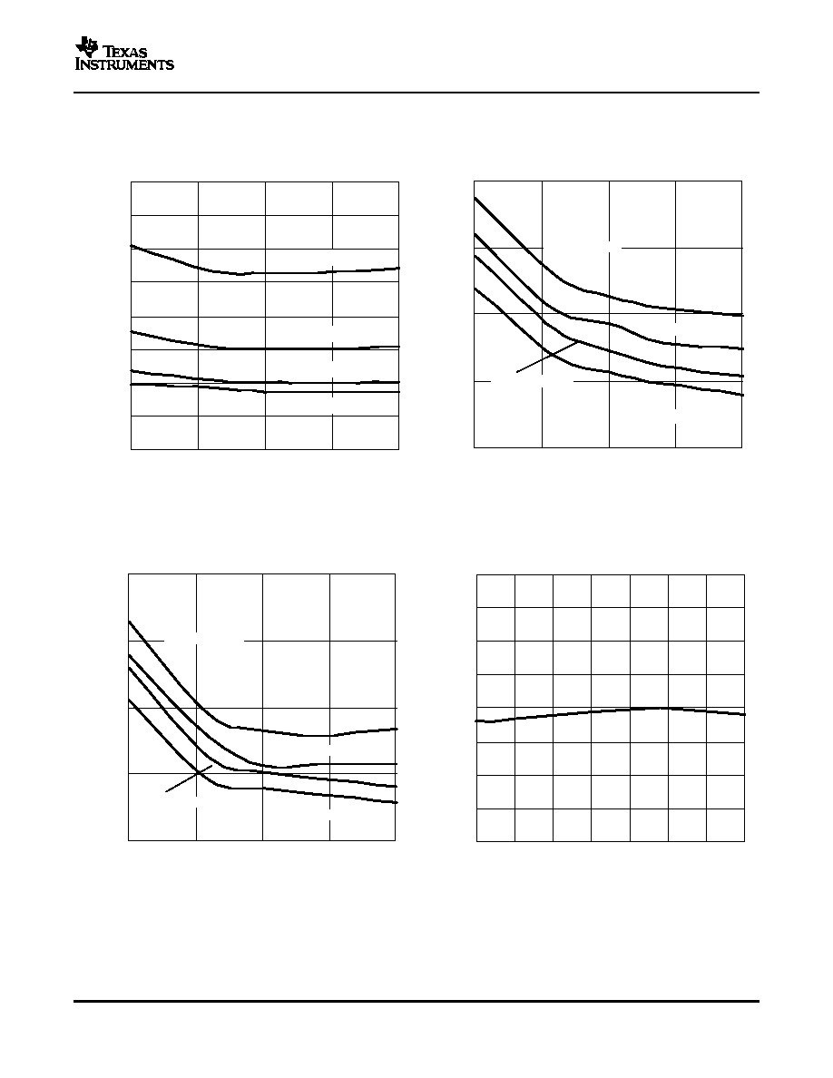
TYPICAL CHARACTERISTICS
!50
50
5.0
4.5
2.5
2.0
1.5
0.5
0.0
!25
0
25
75
100
4.0
1.0
3.5
3.0
UVLO on
UVLO off
UVLO hysteresis
t ! Temperature ! ∞C
125
V
U
V
L
O
!
UVLO Thresholds
!
V
!50
50
5.0
4.5
2.5
2.0
1.5
0.5
0.0
!25
0
25
75
100
4.0
1.0
3.5
3.0
UVLO on
UVLO off
TBD
UVLO hysteresis
t ! Temperature ! ∞C
125
V
U
V
L
O
!
UVLO Thresholds
!
V
!50
50
125
!25
0
25
75
100
20.0
20.5
21.0
21.5
22.0
22.5
23.0
t ! Temperature ! ∞C
I
S
H
O
R
T
_
C
K
T
!
Short Circuit Current
!
mA
VDD = 4.75 V
VDD = 12 V
!50
50
125
!25
0
25
75
100
3.24
3.26
3.28
3.30
3.32
3.34
3.36
t ! Temperature ! ∞C
3V3
!
Reference V
oltage
!
V
UCD8220, UCD8620
SLUS652B ≠ MARCH 2005 ≠ REVISED SEPTEMBER 2005
UCD8220
UCD8620
UVLO THRESHOLD
UVLO THRESHOLD
vs
vs
TEMPERATURE
TEMPERATURE
Figure 8.
Figure 9.
3V3 REFERENCE VOLTAGE
3V3 SHORT-CIRCUIT CURRENT
vs
vs
TEMPERATURE
TEMPERATURE
Figure 10.
Figure 11.
10

www.ti.com
0
1000
1500
500
0
20
40
60
80
100
120
140
160
f ! Frequency ! kHz
I
D
D
!
Supply Current
!
mA
C
LOAD
= 10 nF
C
LOAD
= 4.7 nF
C
LOAD
= 2.2 nF
C
LOAD
= 1 nF
0
40
80
120
160
200
240
280
0
500
1000
1500
f ! Frequency ! kHz
I
D
D
!
Supply Current
!
mA
C
LOAD
= 10 nF
C
LOAD
= 4.7 nF
C
LOAD
= 2.2 nF
C
LOAD
= 1 nF
0
40
80
120
160
200
240
280
320
0
500
1000
1500
f ! Frequency ! kHz
I
D
D
!
Supply Current
!
mA
C
LOAD
= 10 nF
C
LOAD
= 4.7 nF
C
LOAD
= 2.2 nF
C
LOAD
= 1 nF
0
50
100
150
200
250
300
350
400
0
500
1000
1500
f ! Frequency ! kHz
I
D
D
!
Supply Current
!
mA
C
LOAD
= 10 nF
C
LOAD
= 4.7 nF
C
LOAD
= 2.2 nF
C
LOAD
= 1 nF
UCD8220, UCD8620
SLUS652B ≠ MARCH 2005 ≠ REVISED SEPTEMBER 2005
TYPICAL CHARACTERISTICS (continued)
SUPPLY CURRENT
SUPPLY CURRENT
vs
vs
FREQUENCY (V
DD
= 5 V)
FREQUENCY (V
DD
= 8 V)
Figure 12.
Figure 13.
SUPPLY CURRENT
SUPPLY CURRENT
vs
vs
FREQUENCY (V
DD
= 10 V)
FREQUENCY (V
DD
= 12 V)
Figure 14.
Figure 15.
11

www.ti.com
0
50
100
150
200
250
300
350
400
450
500
0
500
1000
1500
f ! Frequency ! kHz
I
D
D
!
Supply Current
!
mA
C
LOAD
= 10 nF
C
LOAD
= 4.7 nF
C
LOAD
= 2.2 nF
C
LOAD
= 1 nF
!50
50
125
!25
0
25
75
100
0.0
0.5
1.0
1.5
2.0
2.5
T
J
! Temperature ! ∞C
V
!
CLK Input V
I
oltage
!
V
CLK Input Rising
CLK Input Falling
5
15
25
35
45
55
65
5
7.5
10
12.5
15
V
DD
! Supply Voltage ! V
t
!
Output Rise T
R
ime
!
ns
C
LOAD
= 10 nF
C
LOAD
= 4.7 nF
C
LOAD
= 2.2 nF
C
LOAD
= 1 nF
!50
50
125
!25
0
25
75
100
0
2
4
6
8
10
12
14
16
18
T
J
! Temperature ! ∞C
t
R
,
t
F
!
Rise and Fall T
imes
!
ns
t
R
= Rise Time
t
F
= Fall Time
C
LOAD
= 2.2 nF
UCD8220, UCD8620
SLUS652B ≠ MARCH 2005 ≠ REVISED SEPTEMBER 2005
TYPICAL CHARACTERISTICS (continued)
SUPPLY CURRENT
CLK INPUT THRESHOLD
vs
vs
FREQUENCY (V
DD
= 15 V)
TEMPERATURE
Figure 16.
Figure 17.
OUTPUT RISE TIME AND FALL TIME
OUTPUT RISE TIME
vs
vs
TEMPERATURE (V
DD
= 12 V)
SUPPLY VOLTAGE
Figure 18.
Figure 19.
12
www.ti.com
0
5
10
15
20
5
7.5
10
12.5
15
V
DD
! Supply Voltage ! V
t
P
D
!
Propagation Delay
, Rising
!
ns
C
LOAD
= 10 nF
C
LOAD
= 4.7 nF
C
LOAD
= 2.2 nF
C
LOAD
= 1 nF
5
10
15
20
25
30
35
40
45
5
7.5
10
12.5
15
V
DD
! Supply Voltage ! V
t
!
Output Fall T
F
ime
!
ns
C
LOAD
= 10 nF
C
LOAD
= 4.7 nF
C
LOAD
= 2.2 nF
C
LOAD
= 1 nF
5
10
15
20
25
5
7.5
10
12.5
15
V
DD
! Supply Voltage ! V
t
P
D
!
Propagation Delay
, Falling
!
ns
C
LOAD
= 10 nF
C
LOAD
= 4.7 nF
C
LOAD
= 2.2 nF
C
LOAD
= 1 nF
!50
50
125
!25
0
25
75
100
0.51
0.52
0.53
0.54
0.55
0.56
0.57
0.58
0.59
T
J
! Temperature ! ∞C
V
C
S
!
Current Limit Threshold
!
V
UCD8220, UCD8620
SLUS652B ≠ MARCH 2005 ≠ REVISED SEPTEMBER 2005
TYPICAL CHARACTERISTICS (continued)
OUTPUT FALL TIME
CLK to OUTx PROPAGATION DELAY RISING
vs
vs
SUPPLY VOLTAGE
SUPPLY VOLTAGE
Figure 20.
Figure 21.
CLK TO OUTx PROPAGATION DELAY FALLING
DEFAULT CURRENT LIMIT THRESHOLD
vs
vs
SUPPLY CURRENT
TEMPERATURE
Figure 22.
Figure 23.
13
www.ti.com
!50
50
!25
0
25
75
100
0
5
10
15
20
25
30
35
40
45
50
T
J
! Temperature ! ∞C
t
P
D
!
CS to CLF Propagation Delay
!
ns
125
!50
50
125
!25
0
25
75
100
0
5
10
15
20
25
30
35
40
T
J
! Temperature ! ∞C
t
P
D
!
CS to OUTx Propagation Delay
!
ns
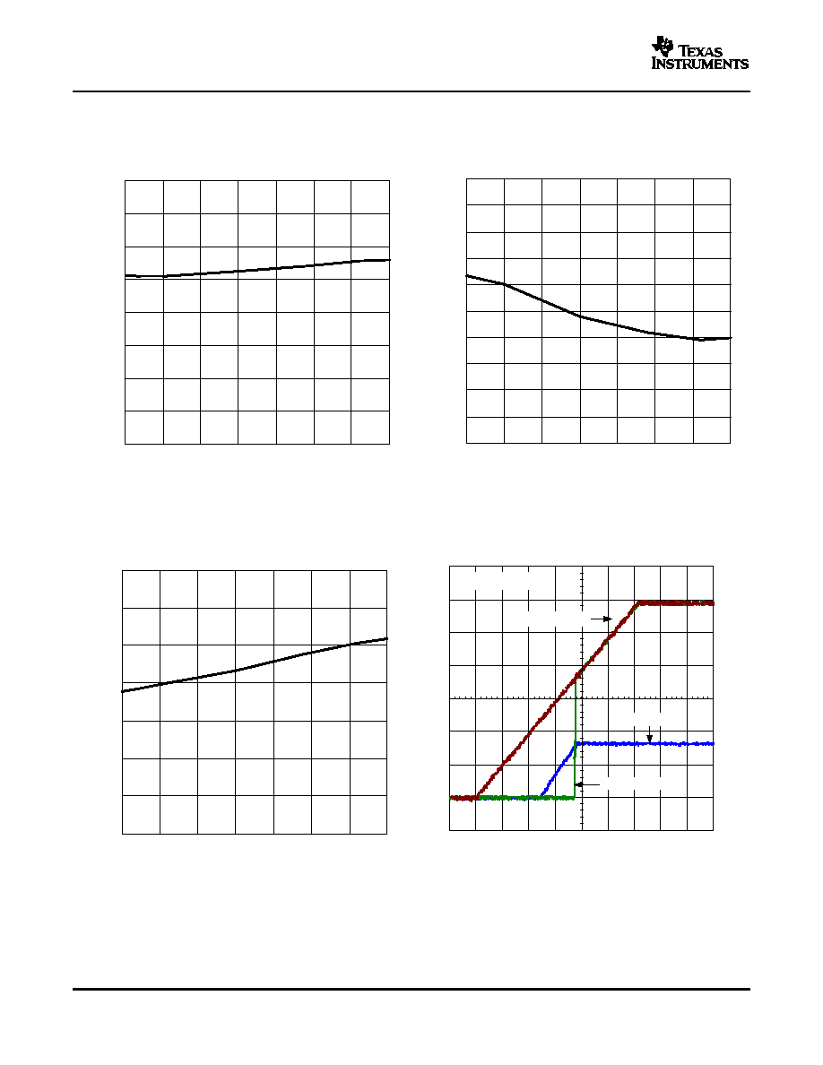
t ! Time ! 40 ms/div
VDD (2 V/div)
CLK = CTRL = 3V3
OUTx (2 V/div)
3V3 (2 V/div)
!50
50
125
!25
0
25
75
100
0
5
10
15
20
25
30
35
T
J
! Temperature ! ∞C
t
P
D
!
Propagation Delay
!
ns
UCD8220, UCD8620
SLUS652B ≠ MARCH 2005 ≠ REVISED SEPTEMBER 2005
TYPICAL CHARACTERISTICS (continued)
CS TO OUTx PROPAGATION DELAY
CS TO CLF PROPAGATION DELAY
vs
vs
TEMPERATURE
TEMPERATURE
Figure 24.
Figure 25.
CLK TO OUT PROPAGATION DELAY
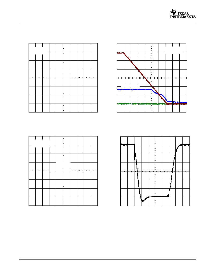
UCD8220
vs
START-UP BEHAVIOR AT V
DD
= 12 V
TEMPERATURE
Figure 26.
Figure 27.
14
www.ti.com
t ! Time ! 40 ms/div
VDD (2 V/div)
OUTx (2 V/div)
3V3 (2 V/div)
CLK = CTRL = 3V3
t ! Time ! 40 ms/div
TBD
CLK = CTRL = 3V3
t ! Time ! 40 ms/div
VDD (2 V/div)
3V3 (2 V/div)
OUTx (2 V/div)
CLK = AGND
CTRL = 3V3
t ! Time ! 40 ms/div
TBD
CLK = CTRL = 3V3
UCD8220, UCD8620
SLUS652B ≠ MARCH 2005 ≠ REVISED SEPTEMBER 2005
TYPICAL CHARACTERISTICS (continued)
UCD8620
UCD8220
START-UP BEHAVIOR AT V
DD
= 12 V
SHUT-DOWN BEHAVIOR AT V
DD
= 12 V
Figure 28.
Figure 29.
UCD8620
UCD8220
SHUT-DOWN BEHAVIOR AT V
DD
= 12 V
START-UP BEHAVIOR AT V
DD
= 12 V
Figure 30.
Figure 31.
15
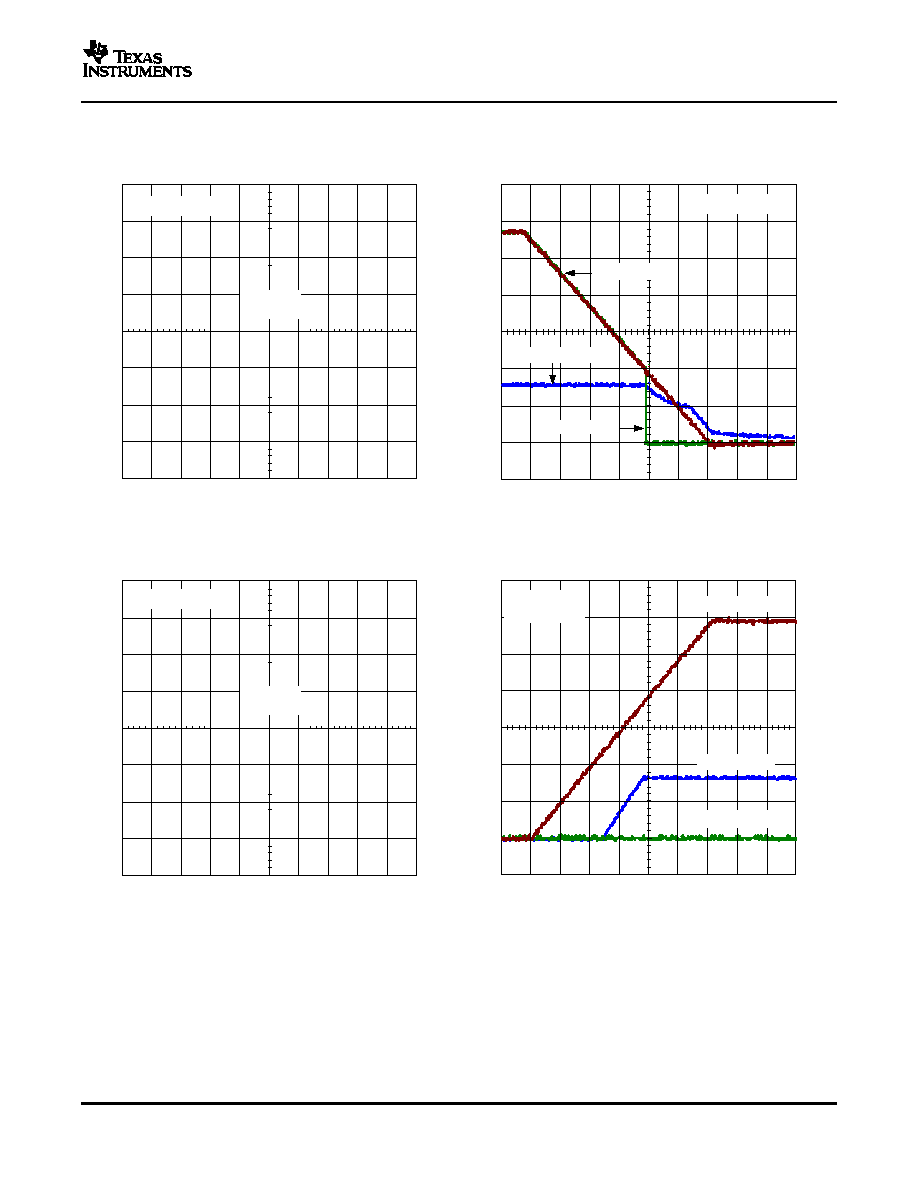
www.ti.com
t ! Time ! 40 ms/div
VDD (2 V/div)
3V3 (2 V/div)
OUTx (2 V/div)
CLK = AGND
CTRL = 3V3
t ! Time ! 40 ms/div
TBD
CLK = AGND
CTRL = 3V3
t ! Time ! 40 ns/div
Output V
oltage
!
2 V/div
t ! Time ! 40 ms/div
TBD
CLK = AGND
CTRL = 3V3
UCD8220, UCD8620
SLUS652B ≠ MARCH 2005 ≠ REVISED SEPTEMBER 2005
TYPICAL CHARACTERISTICS (continued)
UCD8620
UCD8220
START-UP BEHAVIOR AT V
DD
= 12 V
SHUT-DOWN BEHAVIOR AT V
DD
= 12 V
Figure 32.
Figure 33.
UCD8620
OUTPUT RISE AND FALL TIME
SHUT-DOWN BEHAVIOR AT V
DD
= 12 V
(V
DD
= 12 V, C
LOAD
= 10 nF)
Figure 34.
Figure 35.
16

www.ti.com
!50
50
125
!25
0
25
75
100
T
J
! Temperature ! ∞C
Current Mode Slope,
R = 100 k
ISET
0.134
0.136
0.138
0.140
0.142
0.144
0.146
Internal Slope Compensation in CMC - V/
m
s
0.518
0.520
0.522
0.524
0.526
0.528
0.530
0.532
PWM Offset at CTRL
Input
!
V
!50
50
125
!25
0
25
75
100
T
J
! Temperature ! ∞C
!50
50
125
!25
0
25
75
100
T
J
! Temperature ! ∞C
V = 76 V
I
V = 18 V
I
V
= 12 V
DD
Source Current - mA
TBD
UCD8220, UCD8620
SLUS652B ≠ MARCH 2005 ≠ REVISED SEPTEMBER 2005
TYPICAL CHARACTERISTICS (continued)
INTERNAL SLOPE COMPENSATION IN CMC
PWM OFFSET AT CTRL INPUT
vs
vs
TEMPERATURE
TEMPERATURE
Figure 36.
Figure 37.
HIGH VOLTAGE JFET CURRENT
vs
TEMPERATURE
Figure 38.
17

www.ti.com
APPLICATION INFORMATION
UCD8220, UCD8620
SLUS652B ≠ MARCH 2005 ≠ REVISED SEPTEMBER 2005
operating frequency and maximum duty cycle limit
Introduction
and hence controls the power supply operation as
The UCD8220 and UCD8620 are digitally managed
listed above. The pulse train uses a Texas Instru-
analog PWM controllers configured with push-pull
ments communication protocol which is a proprietary
drive logic. The UCD8620 has a 110-V high-voltage
communication system that provides handles for
startup circuit which can directly start up the controller
control
of
the
power
supply
operation
through
from a 48-V telecom input line.
software programming. The rising edge of the CLK
signal represents the switching frequency.
Figure 39
In systems using UCD8K devices, the PWM feedback
depicts the operation of the UCD8K device in one of
loop is closed using the traditional analog methods,
5 modes. At the time when the internal signal REF
but the UCD8K controllers include circuitry to interpret
OK is low, the UCD8K device is not ready to accept
a time-domain digital pulse train from a digital control-
CLK inputs. Once the REF OK signal goes high, then
ler. The pulse train contains the operating frequency
the device is ready to process inputs. While the CLK
and maximum duty cycle limit and hence controls the
input is low, the outputs are disabled and the CLK
power supply operation. This eases implementing a
signal is used as an enable input. Once the Digital
converter with high-level control features without the
controller completes its initialization routine and ver-
added complexity or digital PWM resolution limi-
ifies that all voltages are within their operating range,
tations encountered when closing the voltage control
then it starts the soft-start procedure by slowly
loop in the discrete time domain.
ramping up the duty cycle of the CLK signal, while
maintaining the desired switching frequency. The duty
The UCD8220 and UCD8620 can be configured for
cycle
continues
to
increase
until
it
reaches
either peak current mode or voltage mode control.
steady-state where the analog control loop takes over
They provide a programmable current limit function
and regulates the output voltage to the desire set
and a digital output current limit flag which can be
point. During steady state, the maximum duty cycle
monitored by the host controller. For fast switching
can be set using a volt second product calculation in
speeds, the output stages use the TrueDriveTM output
order to protect the primary of the power transformer
architecture, which delivers rated current of ±4 A into
from saturation during transients. When the power
the gate of a MOSFET during the Miller plateau
supply enters current limit, the outputs are quickly
region of the switching transition. Finally they also
turned off, and the CLF signal is set high in order to
include a 3.3-V, 10-mA linear regulator to provide
notify the digital controller that the last power pulse
power for the digital controller.
was truncated because of an overcurrent event. The
The UCD8620 includes circuitry and features to ease
benefit of this technique is in the flexibility it offers.
implementing a converter that is managed by a
The software is now in charge of the response to
microcontroller or a digital signal processor. Digitally
overcurrent events. In typical analog designs, the
managed
power
supplies
provide
software
power supply response to overcurrent is hardwired in
programmability and monitoring capability of the
the silicon. With this method, the user can configure
power supply operation including:
the response differently for different applications. For
∑
Switching frequency
example, the software can be configured to latch-off
the power supply in response the first overcurrent
∑
Synchronization
event, or to allow a fixed number of current limit
∑
D
MAX
events, so that the supply is capable of starting up
∑
V x S clamp
into a capacitive load. The user can also configure
∑
Input UVLO start/stop voltage
the supply to enter into hiccup mode immediately or
∑
Input OVP start/stop voltage
after a certain number of current limit events. As
described later in this data sheet, the current limit
∑
Soft-start profile
threshold can be varied in time to create unique
∑
Current limit operation
current limit profiles. For example, the current limit set
∑
Shutdown
point can be set high for a predefined number of
∑
Temperature shutdown
cycles to blow a manual fuse, and can be reduced
down to protect the system in the event of a faulty
CLK Input Time-Domain Digital Pulse Train
fuse.
While the loop is closed in the analog domain, the
UCD8K devices are managed by a time-domain
digital pulse train from a digital controller. The pulse
train, shown as CLK in
Figure 39
, contains the
18
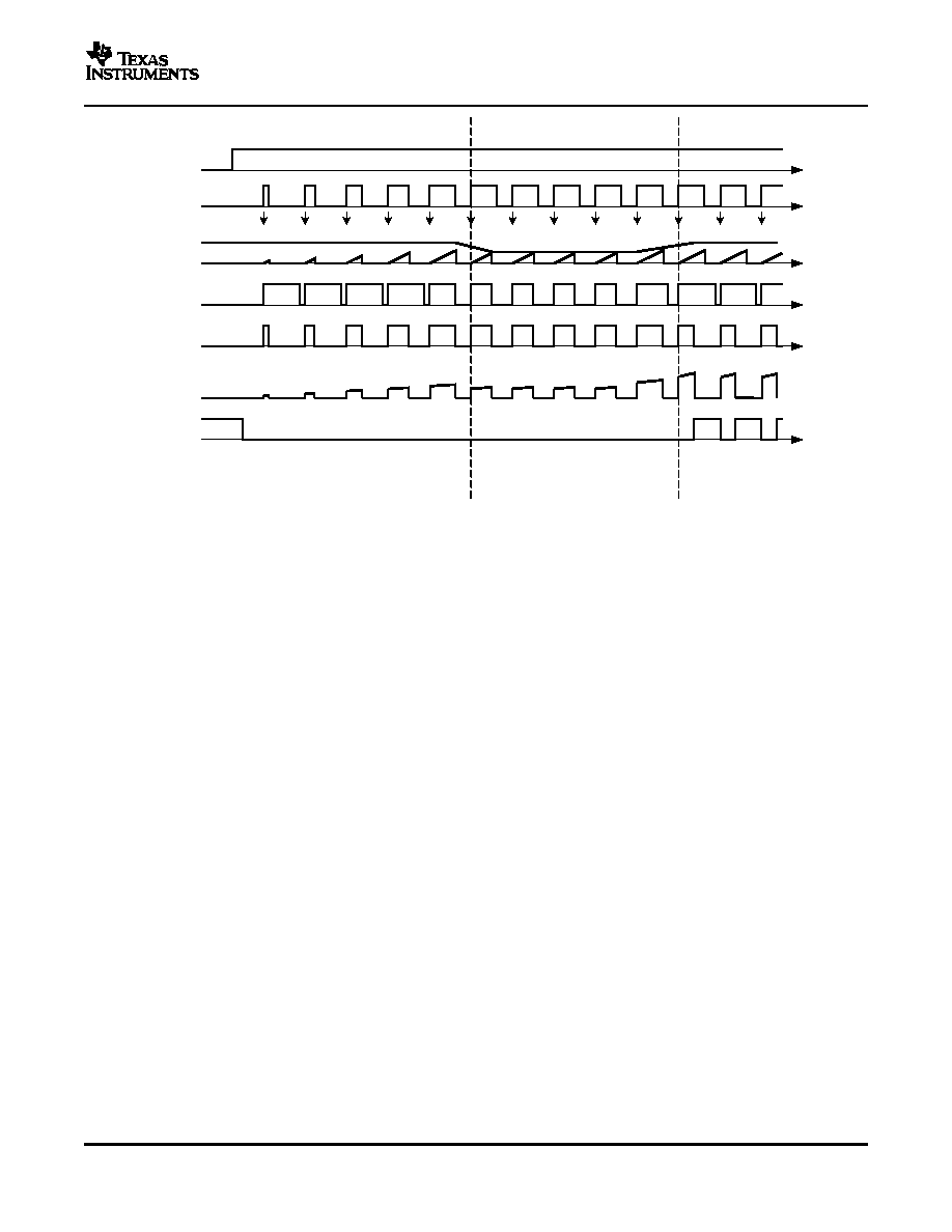
www.ti.com
OUT
RAMP*
CTRL
CLF
CLK
UVLO and
REF OK*
*
- Internal signals
PWM*
Start up
Steady State
Current Limit
CS
UCD8220, UCD8620
SLUS652B ≠ MARCH 2005 ≠ REVISED SEPTEMBER 2005
Figure 39. UCD8220 and UCD8620 Timing and Circuit Operation Diagram
to switch. The JFET remains off provided the outputs
JFET Operation (UCD8620 Only)
are switching and the VDD voltage stays above 7.5
The UCD8620 digitally managed push-pull analog
V. If the VDD voltage drops below 7.5 V while the
PWM Controller contains a 110-V start-up JFET to
outputs are switching, the outputs are immediately
simplify the start-up and standby power requirements
disabled, and the JFET is switched back on. It then
for systems with digital controllers. The JFET circuit
attempts to charge the VDD voltage back up to 13 V.
has two operating modes. When the VDD voltage is
Once the VDD voltage reaches 13 V, the outputs are
less than 5 V, the circuit is limited to 5 mA of source
enabled again and allowed to switch. If the CLK input
current into VDD. The VDD reaches 5 V, the circuit
is not switched by the digital controller, then the VDD
switches into temperature protection mode and pro-
voltage decays to 12 V, and the JFET turns on again.
vides 10 mA until the temperature of the die exceeds
This charges the VDD capacitor back to 13 V where
145
∞
C.
Figure 40
shows the operation of the JET
the cycle repeats until the input voltage drops to a
circuitry
during
various
operating
conditions.
At
point where the VDD voltage can no longer be
start-up, the JFET is on and charges up the VDD
maintained.
Figure 41
shows the graph of available
capacitor. Once the VDD voltage reaches its UVLO of
source current as a function of input and VDD
13 V, the JFET turns off and the outputs are allowed
voltage.
19

www.ti.com
0
2
4
6
8
10
12
14
!50
!40
!30
!20
!10
0
10
16
20
30
TBD
V
- Supply Voltage - V
DD
I
!
Supp;y Current
D
D
!
mA
UCD8220, UCD8620
SLUS652B ≠ MARCH 2005 ≠ REVISED SEPTEMBER 2005
(1)
For VDD to go below 12 V, the input supply must be dropping out.
Figure 40. UCD8620 JFET Operation Waveforms
Reference / External Bias Supply
All devices in the UCD8K family are capable of
supplying a regulated 3.3-V rail to power various
types of external loads such as a microcontroller or
an ASIC. The onboard linear voltage regulator is
capable of sourcing up to 10 mA of current. For
normal operation, place 0.22-µF of ceramic capaci-
tance between the 3V3 pin and the AGND pin.
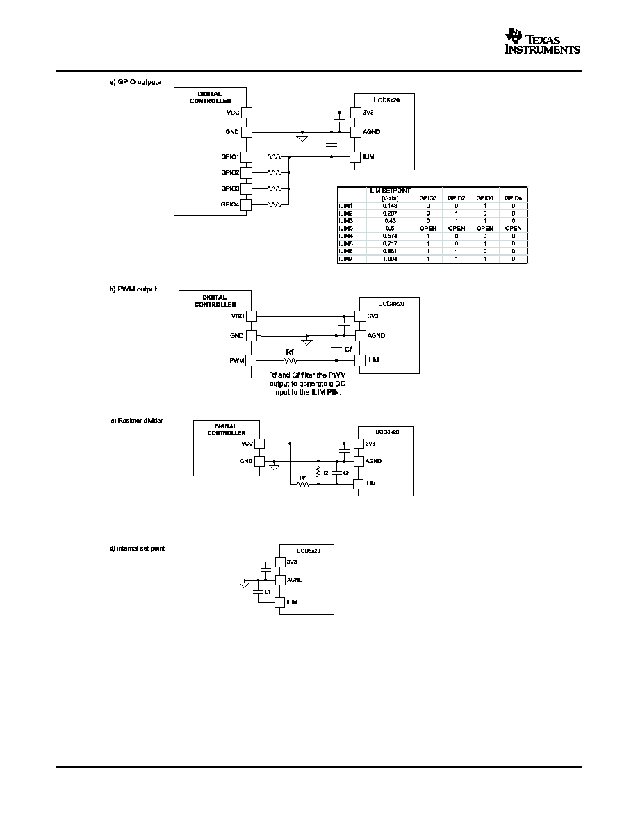
Current Sensing and Protection
Figure 42. Current Sense Filter
Figure 41. UCD8620 Supply Current vs Supply
Voltage
A fast current limit comparator connected to the CS
Supply
pin is used to protect the power stage by im-
plementing cycle-by-cycle current limiting.
Figure 43
The UCD8K devices accept an input range of 4.5 V
shows various methods for setting the ILIM threshold.
to 15.5 V. The device has an internal precision linear
regulator that produces the 3V3 output from this VDD
The current limit threshold may be set to any value
input. A separate pin, PVDD, not connected internally
between 0.25 V and 1 V by applying the desired
to the VDD supply rail provides power for the output
threshold voltage to the current limit (ILIM) pin. If the
drivers. In all applications the same bus voltage must
ILIM pin is left floating, the internal current limit
supply the two pins. It is recommended that a low
threshold is 0.5 V. When the CS level is greater than
value of resistance be placed between the two pins
the ILIM voltage minus 25 mV, the output of the
so that the local capacitance on each pin forms low
driver is forced low and the current limit flag (CLF) is
pass filters to attenuate any switching noise that may
set high. The CLF signal is latched high until the
be on the bus.
UCD8K device receives the next rising edge on the
CLK pin.
20

www.ti.com
UCD8220, UCD8620
SLUS652B ≠ MARCH 2005 ≠ REVISED SEPTEMBER 2005
When the CS voltage is below ILIM, the driver output
restart the device in the event that it is not operating
follows the PWM command. The CLF digital output
properly. But these peripherals typically do not react
flag is monitored by the host controller to determine
fast enough to save the power stage. The UCD87K's
when a current limit event occurs, and to then apply
local current limit comparator provides the required
the appropriate algorithm to obtain the desired current
fast protection for the power stage.
limit profile (i.e. straight line, fold back, hickup, or
The CS threshold is 25 mV below the ILIM voltage. If
latch-off).
the user attempts to command zero current while the
A benefit of this local protection feature is that the
CS pin is at ground, the CLF flag latches high until
UCD8620 devices protects the power stage if the
the CLK pin receives a pulse. At start-up, it is
software code in the digital controller becomes cor-
necessary to ensure that the ILIM pin is always
rupted. If the controller's PWM output stays high, the
greater than the CS pin for the handshaking to work.
local current sense circuit turns off the driver output
If for any reason the CS pin comes to within 25 mV of
when an overcurrent event occurs. The system then
the ILIM pin during start-up, then the CLF flag is
goes into retry mode because most DSP and
latched high and the digital controller must poll the
microcontrollers
have
an
on-board
watchdog,
UCD8620 device, by sending it a narrow CLK pulse.
brown-out, and other supervisory peripherals to
If a fault condition is not present, the CLK pulse
resets the CLF signal to low indicating that the
UCD8620 device is ready to process power pulses.
21
www.ti.com
40 kW
20 kW
10 kW
2.5 kW
UCD8220, UCD8620
SLUS652B ≠ MARCH 2005 ≠ REVISED SEPTEMBER 2005
Figure 43. ILIM Settings
22
www.ti.com
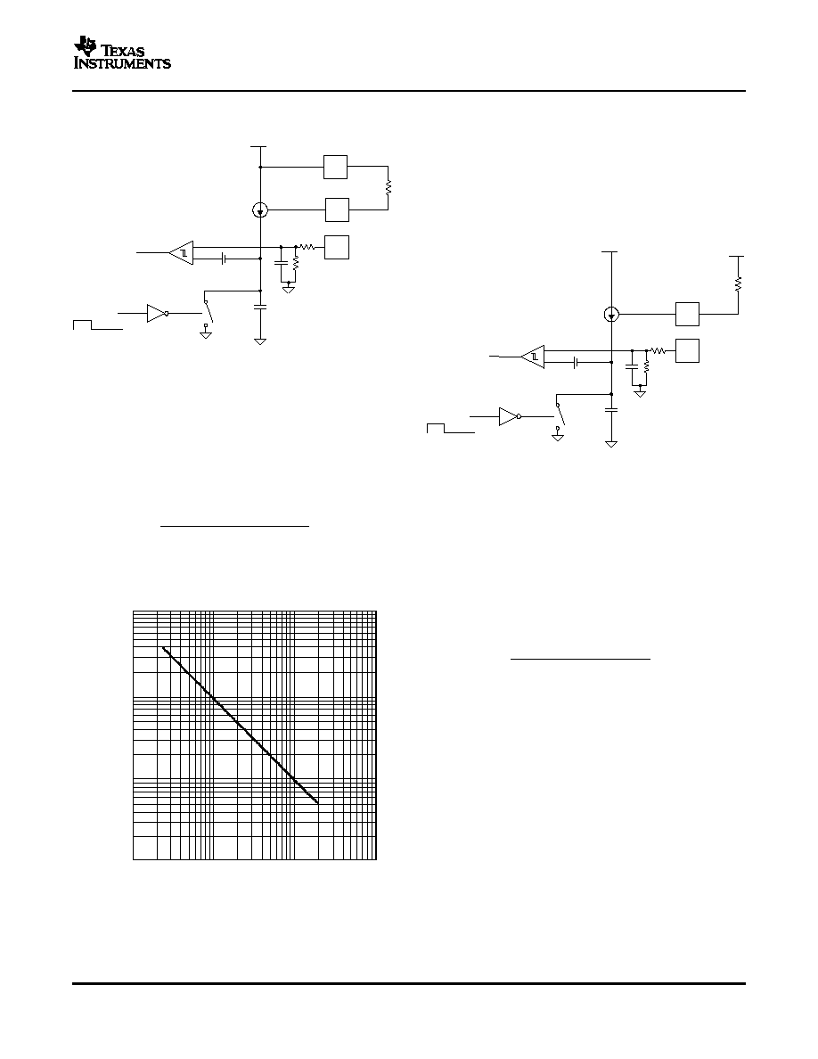
PWM
+
-
3V3
CTRL
(6)
+
ISET
(4)
C
9.4 pF
int
OUT
TO CLEAR
of
PWM LATCH
ON
OFF
I_SC = (3.3 - 1.85) / (11 x R_ISET)
R_ISET
0.25 V
S1
R
R
3V3
(3)
PWM
+
-
3V3
CTRL
(6)
+
ISET
(4)
OUT
ON
OFF
R_ISET
0.25 V
S1
R
R
VIN
C
9.4 pF
int
I_SC = (3.3 - 1.85) / (11 x R_ISET)
TO CLEAR
of
PWM LATCH
11 x 1.4 x fclk x 1000 x 9.4
12
(3.3 - 1.85) x 10
W
R_ISET =
(1)
11 x 1.4 x fclk x 9.4
12
(Vin_max - 1.85) x 10
R_ISET =
W
(2)
1 k
10 k
100 k
1 M
1000
10000
10
100
Clock Frequency ! kHz
R_ISET Resistance
!
W
UCD8220, UCD8620
SLUS652B ≠ MARCH 2005 ≠ REVISED SEPTEMBER 2005
Selecting the ISET Resistor for Voltage Mode
Figure 45
shows the nominal value of resistance to
Control
use for a desired clock frequency. Note that for the
UCD8220 and the UCD8620 controllers, which have
two outputs controlled by Push-Pull logic, the output
ripple frequency is equal to the clock frequency; and
each output switches at half the clock frequency.
Selecting the ISET Resistor for Voltage Mode
Control with Voltage Feed forward
Figure 44. UCD8x20 Configured in Voltage Mode
Control with an Internal Timing Capacitor
When the ISET resistor is configured as shown in
Figure 44
with the ISET resistor connected between
the ISET pin and the 3V3 pin, the device is set-up for
voltage mode control. For purposes of voltage loop
Figure 46. UCD8x20 Configured in Voltage Mode
compensation the, voltage ramp is 1.4 V from the
Control with Voltage Feed Forward
valley to the peak. See
Equation 1
for selecting the
proper resistance for a desired clock frequency.
When the ISET resistor is configured as shown in
Figure 46
with the ISET resistor connected between
the ISET pin and the input voltage, VIN, the device is
Where:
configured for voltage mode control with voltage feed
forward. For the purposes of voltage loop compen-
fclk = Desired Clock Frequency in Hz.
sation, the voltage ramp is 1.4 x Vin/Vin_max Volts
from the valley to the peak. See
Equation 2
for
selecting the proper resistance for a desired clock
frequency and input voltage range.
Where:
fclk = Desired Clock Frequency in Hz.
For a general discussion of the benefits of Voltage
Mode Control with Voltage feed forward, see Refer-
ence [5].
Figure 45. ISET Resistance vs Clock Frequency
23

www.ti.com
CS
(9)
+
-
3V3
+
OUT
ON
OFF
S1
S2
R
R
CTRL
(6)
ISET
(4)
R_ISET
PWM
0.25 V
C
12 pF
int
I_SC = 1.85 / (11 x R_ISET)
TO CLEAR
of
PWM LATCH
11 x R_ISET x 12
V/ s
m
6
1.85 x 10
SLOPE =
(3)
0.01
0.1
1
10
100
1 k
10 k
1 k
10 k
100 k
1 M
10
1
100
R_ISET Resistance - W
Slope - V/
s
m
UCD8220, UCD8620
SLUS652B ≠ MARCH 2005 ≠ REVISED SEPTEMBER 2005
Selecting the ISET Resistor for Peak Current
The amount of slope compensation required depends
Mode Control with Internal Slope Compensation
on the design of the power stage and the output
specifications. A general rule is to add an up-slope
equal to the down slope of the output inductor.
Handshaking
The UCD8K family of devices have a built-in hand-
shaking feature to facilitate efficient start-up of the
digitally managed power supply. At start-up the CLF
flag is held high until all the internal and external
supply voltages of the UCD8K device are within their
operating range. Once the supply voltages are within
acceptable limits, the CLF goes low and the device
processes the CLK signals. The digital controller
should monitor the CFL flag at start-up and wait for
the CLF flag to go LOW before sending CLK pulses
to the UCD8K device.
Driver Output
Figure 47. UCCD8x20 Configured in Peak Current
The high-current output stage of the UCD8K device
Control with Internal Slope Compensation
family is capable of supplying ±4-A peak current
pulses and swings to both PVDD and PGND.
When the ISET resistor is configured as shown in
The
drive
output
uses
the
Texas
Instruments
Figure 47
with the ISET resistor connected between
TrueDriveTM architecture, which delivers rated current
the ISET pin and AGND, the device is configured for
into the gate of a MOSFET when it is most needed,
peak current mode control with internal slope com-
during the Miller plateau region of the switching
pensation. The voltage at the ISET pin is 1.85 volts
transition providing efficiency gains.
so the internal slope compensation current, I_SC,
being fed into the internal slope compensation ca-
TrueDriveTM consists of pull-up/pull-down circuits with
pacitor is equal to 1.85 / (11x R_ISET). The voltage
bipolar and MOSFET transistors in parallel. The peak
slope at the PWM comparator input which is gener-
output current rating is the combined current from the
ated by this current is equal to:
bipolar and MOSFET transistors. This hybrid output
stage also allows efficient current sourcing at low
supply voltages.
Source/Sink Capabilities During Miller Plateau
Large power MOSFETs present a large load to the
control circuitry. Proper drive is required for efficient,
reliable operation. The UCD8K drivers have been
optimized to provide maximum drive to a power
MOSFET during the Miller plateau region of the
switching transition. This interval occurs while the
drain voltage is swinging between the voltage levels
dictated by the power topology, requiring the charg-
ing/discharging of the drain-gate capacitance with
current supplied or removed by the driver device. See
Reference [2].
Drive Current and Power Requirements
The UCD8620 family of controllers contains drivers
which can deliver high current into a MOSFET gate
for a period of several
hundred
nanoseconds.
High-peak current is required to turn on a MOSFET.
Then, to turn off a MOSFET, the driver is required to
sink a similar amount of current to ground. This
Figure 48. Slope vs RISET Resistance
repeats at the operating frequency of the power
device.
24

www.ti.com
E =
1
2
2
x CV
(4)
P = CV x 1
2
(5)
P = 2.2 nF x 12 x 300 kHz = 0.095 W
2
(6)
I =
=
P
V
0.095 W
12 V
= 7.9 mA
(7)
UCD8220, UCD8620
SLUS652B ≠ MARCH 2005 ≠ REVISED SEPTEMBER 2005
Reference [2] discusses the current required to drive
ture range the package must allow for the efficient
a
power
MOSFET
and
other
capacitive-input
removal of the heat produced while keeping the
switching devices.
junction temperature within rated limits. The UCD8K
family of drivers is available in PowerPADTM TSSOP
When a driver device is tested with a discrete,
and QFN/DFN packages to cover a range of appli-
capacitive load it is a fairly simple matter to calculate
cation requirements. Both have an exposed pad to
the power that is required from the bias supply. The
enhance thermal conductivity from the semiconductor
energy that must be transferred from the bias supply
junction.
to charge the capacitor is given by:
As illustrated in Reference [3], the PowerPADTM
packages offer a leadframe die pad that is exposed at
the base of the package. This pad is soldered to the
where C is the load capacitor and V is the bias
copper on the PC board (PCB) directly underneath
voltage feeding the driver.
the device package, reducing the
JA
down to
37.47∞C/W. The PC board must be designed with
There is an equal amount of energy transferred to
thermal lands and thermal vias to complete the heat
ground when the capacitor is discharged. This leads
removal subsystem, as summarized in Reference [4].
to a power loss given by the following:
Note that the PowerPADTM is not directly connected
to any leads of the package. However, it is electrically
where f is the switching frequency.
and thermally connected to the substrate which is the
ground of the device. The PowerPADTM should be
This power is dissipated in the resistive elements of
connected to the quiet ground of the circuit.
the circuit. Thus, with no external resistor between
the driver and gate, this power is dissipated inside the
Circuit Layout Recommendations
driver. Half of the total power is dissipated when the
capacitor is charged, and the other half is dissipated
In a MOSFET driver operating at high frequency, it is
when the capacitor is discharged.
critical to minimize stray inductance to minimize
overshoot/undershoot and ringing. The low output
With V
DD
= 12 V, C
LOAD
= 2.2 nF, and f = 300 kHz,
impedance of the drivers produces waveforms with
the power loss can be calculated as:
high di/dt. This tends to induce ringing in the parasitic
inductances. It is advantageous to connect the driver
device close to the MOSFETs. It is recommended
With a 12-V supply, this would equate to a current of:
that the PGND and the AGND pins be connected to
the PowerPADTM of the package with a thin trace. It
is critical to ensure that the voltage potential between
these two pins does not exceed 0.3 V. The use of
Thermal Information
schottky diodes on the outputs to PGND and PVDD is
recommended when driving gate transformers.
The useful range of a driver is greatly affected by the
drive power requirements of the load and the thermal
characteristics of the device package. In order for a
power driver to be useful over a particular tempera-
25

www.ti.com
REFERENCES
RELATED PRODUCTS
REVISION HISTORY
UCD8220, UCD8620
SLUS652B ≠ MARCH 2005 ≠ REVISED SEPTEMBER 2005
1. Power Supply Seminar SEM-1600 Topic 6: A Practical Introduction to Digital Power Supply Control, by
Laszlo Balogh, Texas Instruments Literature No. SLUP224
2. Power Supply Seminar SEM≠1400 Topic 2: Design And Application Guide For High Speed MOSFET Gate
Drive Circuits, by Laszlo Balogh, Texas Instruments Literature No. SLUP133.
3. Technical Brief, PowerPad Thermally Enhanced Package, Texas Instruments Literature No. SLMA002
4. Application Brief, PowerPADTM Made Easy, Texas Instruments Literature No. SLMA004
5. Power Supply Seminar SEM-300 Topic 2, "Closing the Feedback Loop", by Lloyd Dixon Jr., Texas
Instruments, (Literature Number SLUP068)
PRODUCT
DESCRIPTION
FEATURES
UCD9501
Digital Power Controller for High Performance Multi-loop Applications
MSP430F1232
Microcontroller
DATE
REVISION
CHANGE DESCRIPTION
03/05
SLUS652
Initial release.
08/05
SLUS652A
Extensive changes throughout
09/05
SLUS652B
Extensive changes throughout
26
PACKAGING INFORMATION
Orderable Device
Status
(1)
Package
Type
Package
Drawing
Pins Package
Qty
Eco Plan
(2)
Lead/Ball Finish
MSL Peak Temp
(3)
UCD8220PWP
PREVIEW
HTSSOP
PWP
16
90
TBD
Call TI
Call TI
UCD8220PWPR
PREVIEW
HTSSOP
PWP
16
2000
TBD
Call TI
Call TI
UCD8220RSA
PREVIEW
QFN
RSA
16
250
TBD
Call TI
Call TI
UCD8220RSAR
PREVIEW
QFN
RSA
16
3000
TBD
Call TI
Call TI
UCD8620PWP
PREVIEW
HTSSOP
PWP
16
90
TBD
Call TI
Call TI
UCD8620PWPR
PREVIEW
HTSSOP
PWP
16
2000
TBD
Call TI
Call TI
UCD8620RGWR
PREVIEW
QFN
RGW
20
3000
TBD
Call TI
Call TI
UCD8620RGWT
PREVIEW
QFN
RGW
20
250
TBD
Call TI
Call TI
(1)
The marketing status values are defined as follows:
ACTIVE: Product device recommended for new designs.
LIFEBUY: TI has announced that the device will be discontinued, and a lifetime-buy period is in effect.
NRND: Not recommended for new designs. Device is in production to support existing customers, but TI does not recommend using this part in
a new design.
PREVIEW: Device has been announced but is not in production. Samples may or may not be available.
OBSOLETE: TI has discontinued the production of the device.
(2)
Eco
Plan
-
The
planned
eco-friendly
classification:
Pb-Free
(RoHS)
or
Green
(RoHS
&
no
Sb/Br)
-
please
check
http://www.ti.com/productcontent
for the latest availability information and additional product content details.
TBD: The Pb-Free/Green conversion plan has not been defined.
Pb-Free (RoHS): TI's terms "Lead-Free" or "Pb-Free" mean semiconductor products that are compatible with the current RoHS requirements
for all 6 substances, including the requirement that lead not exceed 0.1% by weight in homogeneous materials. Where designed to be soldered
at high temperatures, TI Pb-Free products are suitable for use in specified lead-free processes.
Green (RoHS & no Sb/Br): TI defines "Green" to mean Pb-Free (RoHS compatible), and free of Bromine (Br) and Antimony (Sb) based flame
retardants (Br or Sb do not exceed 0.1% by weight in homogeneous material)
(3)
MSL, Peak Temp. -- The Moisture Sensitivity Level rating according to the JEDEC industry standard classifications, and peak solder
temperature.
Important Information and Disclaimer:The information provided on this page represents TI's knowledge and belief as of the date that it is
provided. TI bases its knowledge and belief on information provided by third parties, and makes no representation or warranty as to the
accuracy of such information. Efforts are underway to better integrate information from third parties. TI has taken and continues to take
reasonable steps to provide representative and accurate information but may not have conducted destructive testing or chemical analysis on
incoming materials and chemicals. TI and TI suppliers consider certain information to be proprietary, and thus CAS numbers and other limited
information may not be available for release.
In no event shall TI's liability arising out of such information exceed the total purchase price of the TI part(s) at issue in this document sold by TI
to Customer on an annual basis.
PACKAGE OPTION ADDENDUM
www.ti.com
23-Sep-2005
Addendum-Page 1

PACKAGING INFORMATION
Orderable Device
Status
(1)
Package
Type
Package
Drawing
Pins Package
Qty
Eco Plan
(2)
Lead/Ball Finish
MSL Peak Temp
(3)
UCD8220PWP
ACTIVE
HTSSOP
PWP
16
90
Green (RoHS &
no Sb/Br)
CU NIPDAU
Level-2-260C-1 YEAR
UCD8220PWPR
ACTIVE
HTSSOP
PWP
16
2000 Green (RoHS &
no Sb/Br)
CU NIPDAU
Level-2-260C-1 YEAR
UCD8220RSA
PREVIEW
QFN
RSA
16
250
TBD
Call TI
Call TI
UCD8220RSAR
PREVIEW
QFN
RSA
16
3000
TBD
Call TI
Call TI
UCD8620PWP
PREVIEW
HTSSOP
PWP
16
90
TBD
Call TI
Call TI
UCD8620PWPR
PREVIEW
HTSSOP
PWP
16
2000
TBD
Call TI
Call TI
UCD8620RGWR
PREVIEW
QFN
RGW
20
3000
TBD
Call TI
Call TI
UCD8620RGWT
PREVIEW
QFN
RGW
20
250
TBD
Call TI
Call TI
(1)
The marketing status values are defined as follows:
ACTIVE: Product device recommended for new designs.
LIFEBUY: TI has announced that the device will be discontinued, and a lifetime-buy period is in effect.
NRND: Not recommended for new designs. Device is in production to support existing customers, but TI does not recommend using this part in
a new design.
PREVIEW: Device has been announced but is not in production. Samples may or may not be available.
OBSOLETE: TI has discontinued the production of the device.
(2)
Eco
Plan
-
The
planned
eco-friendly
classification:
Pb-Free
(RoHS)
or
Green
(RoHS
&
no
Sb/Br)
-
please
check
http://www.ti.com/productcontent
for the latest availability information and additional product content details.
TBD: The Pb-Free/Green conversion plan has not been defined.
Pb-Free (RoHS): TI's terms "Lead-Free" or "Pb-Free" mean semiconductor products that are compatible with the current RoHS requirements
for all 6 substances, including the requirement that lead not exceed 0.1% by weight in homogeneous materials. Where designed to be soldered
at high temperatures, TI Pb-Free products are suitable for use in specified lead-free processes.
Green (RoHS & no Sb/Br): TI defines "Green" to mean Pb-Free (RoHS compatible), and free of Bromine (Br) and Antimony (Sb) based flame
retardants (Br or Sb do not exceed 0.1% by weight in homogeneous material)
(3)
MSL, Peak Temp. -- The Moisture Sensitivity Level rating according to the JEDEC industry standard classifications, and peak solder
temperature.
Important Information and Disclaimer:The information provided on this page represents TI's knowledge and belief as of the date that it is
provided. TI bases its knowledge and belief on information provided by third parties, and makes no representation or warranty as to the
accuracy of such information. Efforts are underway to better integrate information from third parties. TI has taken and continues to take
reasonable steps to provide representative and accurate information but may not have conducted destructive testing or chemical analysis on
incoming materials and chemicals. TI and TI suppliers consider certain information to be proprietary, and thus CAS numbers and other limited
information may not be available for release.
In no event shall TI's liability arising out of such information exceed the total purchase price of the TI part(s) at issue in this document sold by TI
to Customer on an annual basis.
PACKAGE OPTION ADDENDUM
www.ti.com
3-Oct-2005
Addendum-Page 1


IMPORTANT NOTICE
Texas Instruments Incorporated and its subsidiaries (TI) reserve the right to make corrections, modifications,
enhancements, improvements, and other changes to its products and services at any time and to discontinue
any product or service without notice. Customers should obtain the latest relevant information before placing
orders and should verify that such information is current and complete. All products are sold subject to TI's terms
and conditions of sale supplied at the time of order acknowledgment.
TI warrants performance of its hardware products to the specifications applicable at the time of sale in
accordance with TI's standard warranty. Testing and other quality control techniques are used to the extent TI
deems necessary to support this warranty. Except where mandated by government requirements, testing of all
parameters of each product is not necessarily performed.
TI assumes no liability for applications assistance or customer product design. Customers are responsible for
their products and applications using TI components. To minimize the risks associated with customer products
and applications, customers should provide adequate design and operating safeguards.
TI does not warrant or represent that any license, either express or implied, is granted under any TI patent right,
copyright, mask work right, or other TI intellectual property right relating to any combination, machine, or process
in which TI products or services are used. Information published by TI regarding third-party products or services
does not constitute a license from TI to use such products or services or a warranty or endorsement thereof.
Use of such information may require a license from a third party under the patents or other intellectual property
of the third party, or a license from TI under the patents or other intellectual property of TI.
Reproduction of information in TI data books or data sheets is permissible only if reproduction is without
alteration and is accompanied by all associated warranties, conditions, limitations, and notices. Reproduction
of this information with alteration is an unfair and deceptive business practice. TI is not responsible or liable for
such altered documentation.
Resale of TI products or services with statements different from or beyond the parameters stated by TI for that
product or service voids all express and any implied warranties for the associated TI product or service and
is an unfair and deceptive business practice. TI is not responsible or liable for any such statements.
Following are URLs where you can obtain information on other Texas Instruments products and application
solutions:
Products
Applications
Amplifiers
amplifier.ti.com
Audio
www.ti.com/audio
Data Converters
dataconverter.ti.com
Automotive
www.ti.com/automotive
DSP
dsp.ti.com
Broadband
www.ti.com/broadband
Interface
interface.ti.com
Digital Control
www.ti.com/digitalcontrol
Logic
logic.ti.com
Military
www.ti.com/military
Power Mgmt
power.ti.com
Optical Networking
www.ti.com/opticalnetwork
Microcontrollers
microcontroller.ti.com
Security
www.ti.com/security
Telephony
www.ti.com/telephony
Video & Imaging
www.ti.com/video
Wireless
www.ti.com/wireless
Mailing Address:
Texas Instruments
Post Office Box 655303 Dallas, Texas 75265
Copyright
2005, Texas Instruments Incorporated