UCD9112
DIGITAL DUAL PHASE SYNCHRONOUS BUCK CONTROLLER
VER. 0.5 SEPTEMBER 2006
1
Copyright
©
2001, Texas Instruments Incorporated
PRODUCT PREVIEW information concerns products in the
formative or design phase of development. Characteristic data
and other specifications are design goals. Texas Instruments
reserves the right to change or discontinue these products
without notice.
www.ti.com
∑ FEATURES
∑ Digital dual phase synchronous buck
PWM controller with 175ps PWM
resolution
∑ Digital control with programmable PID
compensation
∑ Dual-phase with current balancing
capability
∑ Vin from 4.5V to 14.5V (UCD7230)
∑ Vout from 1% to 99% of Vin
∑ Programmable switching frequency,
capable of up to 2MHz/Phase
∑ Programmable soft start and soft stop
∑ Supports pre-biased start-up
∑ Internally trimmed 0.5% 800mV
Reference
∑ Remote sensing differential amplifier
∑ Power supply monitoring via PMBus
∑ Single bias supply (3.3V VDD)
∑ Graphical user interface configuration
∑ Internal thermal sensor
∑ PMBus Support
Query Voltage, Current, Faults, etc
Voltage Setting and Calibration
Protection Threshold Adjustment
∑ 32-Pin QFN Package
∑ APPLICATIONS
∑
∑ Networking Equipment
∑ Servers
∑ Storage Systems
∑ Telecommunications Equipment
∑ DC Power Distributed Systems
∑ Industrial / ATE
∑ DESCRIPTION
The UCD9112 is dual-phase synchronous buck
digital PWM controller that supports point of load
(POL) applications. The device is configured thru
the use of a graphical user interface (GUI). The loop
compensator is configurable with the GUI to meet
dynamic converter performance allowing a single
hardware design to cover a broad range of POL
applications.
In addition to digital control loop, the UCD9112 is
able to monitor and manage power supply operating
conditions and report the status to the host system
through PMBus. The management parameters are
configurable through GUI. The GUI also allows the
power supply designer to easily configure the digital
control loop characteristics and generate the gain
and phase information for analysis using bode plots.
To ensure balanced outputs on each phase, the
UCD9112 incorporates a current balancing scheme.
The PWM output of the dual phase controller is
capable of operating at a switching frequency of up
to 2MHz with a relative phase adjustment of 180
o
.
The UCD7230 synchronous buck driver has been
designed to work with the UCD9112 controller to
provide a highly integrated digital power solution. In
addition to 4A output drive capability, the driver
integrates current limit, short circuit protection as well
as under-voltage lockout protection. The UCD7230
also has a 3.3V, 10mA linear regulator that provides
the supply current for the controller
.
ORDERING INFORMATION
PACKAGE
TAPE AND REEL QTY
PART NUMBER
QFN 250
UCD9112RHB

UCD9112
DIGITAL DUAL PHASE SYNCHRONOUS BUCK CONTROLLER
VER. 0.5 SEPTEMBER 2006
2
Copyright
©
2001, Texas Instruments Incorporated
PRODUCT PREVIEW information concerns products in the
formative or design phase of development. Characteristic data
and other specifications are design goals. Texas Instruments
reserves the right to change or discontinue these products
without notice.
www.ti.com
Table of Contents
Features
1
Device
Information
3
1.1 System Block Diagram
4
1.2 Example Dual Phase Implementation
5
1.3
Pin
Assignment
5
1.4
Pin
Functions
5
2
Device
Ratings
7
2.1 Absolute Maximum Ratings
7
2.2 Recommended Operating Conditions
7
2.3 Electronic Discharge (ESD) Protection
7
3
Electrical
Characteristics
8
4 Typical Characteristics
11
5
Function
Overview
11
5.1
Reset
11
5.1.1 Power-on Reset
11
5.1.2 Brown-out Reset
11
5.1.3
Watchdog
11
5.1.4 External Reset
11
5.2
Analog
Inputs
12
5.2.1
Resolution
12
5.2.2 Input Impedance
12
5.3
PMBus
Address
13
5.4
PID
Compensator
14
5.5 Output Voltage Sensing
15
6
PMBus
interface
16
6.1
PMBus
Timing
16
6.2 Output Configuration Commands
16
6.2.1 Remote ON/OFF
16
6.2.2 Output Voltage Set Point
16
6.2.3 Output Voltage Calibration
17
6.2.4 Margin up/down
17
6.2.5 Output Current Measurement
17
6.2.6 Start up into Pre-Bias
18
6.2.7 Output Voltage Sequencing
18
6.2.8 Output Voltage Soft Start
19
6.2.9 Output Voltage Soft Stop
19
6.2.10 Power Good (PGOOD)
20
6.3 Protection Commands
20
6.3.1 Input Under Voltage Protection
20
6.3.2 Input Over Voltage Protection
21
6.3.3 Output Over Voltage Protection
21
6.3.4 Output Under Voltage Protection
22
6.3.5 Output Over Current Protection
23
6.3.6 Over Temperature Protection
23
6.4 Status & Fault Reporting Commands
24
6.5 Non-Volatile Storage Commands
24
6.6 Host data Storage Commands
25
7 Dual Phase Current Balancing
25
8 GUI
26
9
Package
Information
29
List of Figures
Figure 1-1 UCD9112 Block Diagram
3
Figure 1-2. UCD9112 with the UCD7230
4
Figure 1-3. UCD9112 Pin Assignment
5
Figure 3-1 PMBus Timing Diagram
10
Figure 5-1 V
addr
to PMBus address translation
13
Figure 5-2 Output voltage sensing circuitry
15
Figure 6-1 Current Gain and Offset
18
Figure 8-1 GUI Interface for POL Configuration 27
Figure 9-1 32-Pin PowerPAD
TM
QFN Package 29
List of Tables
Table 1-1 UCD9112 Pin Descriptions
5
Table 5-1Device reset voltage threshold
11
Table 5-2 Analog input assignments
12
Table 5-4 Configuration of PMBus addresses
14
Table 7-1 Current balancing of two phases
26

UCD9112
DIGITAL DUAL PHASE SYNCHRONOUS BUCK CONTROLLER
VER. 0.5 SEPTEMBER 2006
3
Copyright
©
2001, Texas Instruments Incorporated
PRODUCT PREVIEW information concerns products in the
formative or design phase of development. Characteristic data
and other specifications are design goals. Texas Instruments
reserves the right to change or discontinue these products
without notice.
www.ti.com
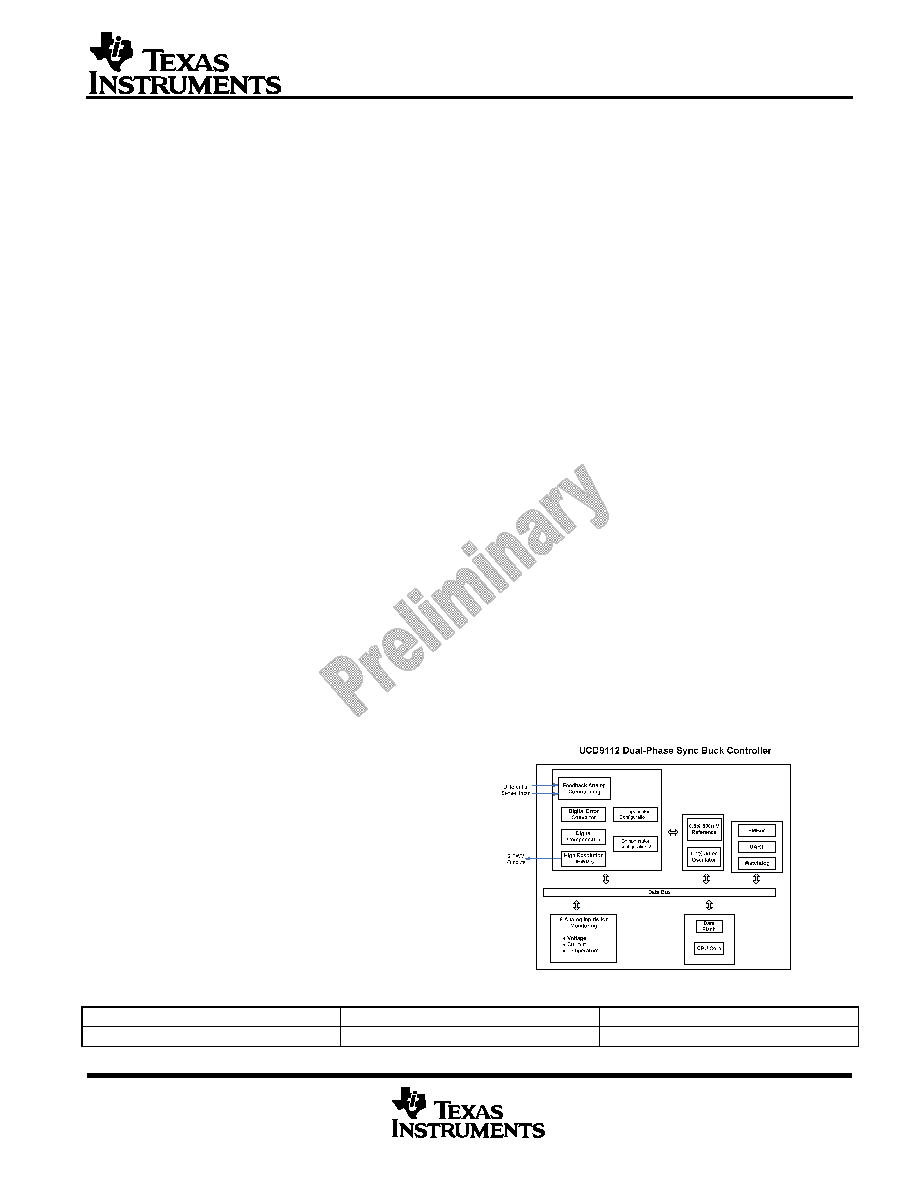
1 DEVICE INFORMATION
1.1 BLOCK DIAGRAM
Figure 1-1. UCD9112 Block Diagram
UCD9112
SEPTEMBER 2006
4
www.ti.com
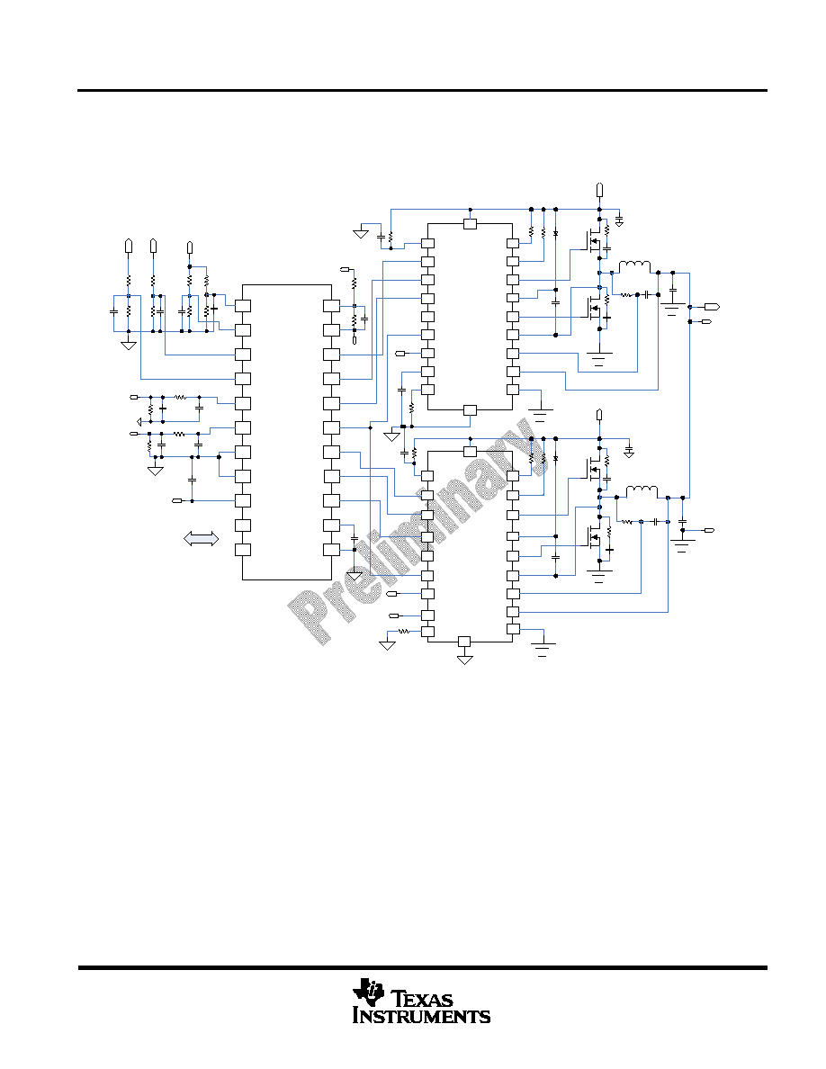
1.2 EXAMPLE DUAL PHASE IMPLEMENTATION WITH THE UCD7230 DRIVER
OUT2
NEG
BST
POS
PGND
AGND
SRE
CLF
ILIM
UCD7230
Iout0
PMBus Commun
IN
CS+
3V3
Vout
UCD9112
ADDR1
ADDR0
IOUT_0
VIN
VOUT
IOUT_1
DVSS
DV25
RST
EAP
ILIM
DPWM1A
DPWM0B
DPWM0A
DPWM1B
CLK
DATA
CLF1
EAN
CLF0
VD33
AVSS
AO
VDD
CS BIAS
PVDD
OUT1
IO
OUT2
NEG
BST
POS
PGND
AGND
SRE
CLF
ILIM
IN
CS+
3V3
AO
VDD
CS BIAS
PVDD
OUT1
IO
SW
SW
UCD7230
Vin
Vin
Vin
Vout
3.3V
Iout1
VD33
Iout0
VD33
Iout1
RS-
RS+
R1
R2
R3
R4
R10
R8
R7
R6
R5
C11
R11
R9
R12
R13
R14
R15
R16 R17
R18
R19
R20 R21
C1
C2
C3
C4
C10
C9
C8
C7
C6
C5
C12
C13
C14
C15
C16
C17
C18
C19
C20
R22
R23
R24
R25
C21
C22
C23
C24
C25
C26
R26
Q1
Q2
D1
Q3
D2
Q4
L1
L2
RS+
RS-
R27
R28
DLY
DLY
Figure 1-2. UCD9112 in a Dual Phase Configuration
UCD9112
SEPEMBER 2006
5
www.ti.com
1.2 PIN ASSIGNMENTS
Figure 1-3. UCD9112 QFN Package Pin Assignments
1.3 PIN FUNCTIONS
Table 1.1 UCD9112 Pin Descriptions
TERMINAL PIN
NAME NO.
I/O
A/D
DESCRIPTION
ADDR1 1
I
A
ADDR0 2
I
A
Addr1 and Addr0 signals are analog voltage that are sampled when
UCD9112 is released from reset. The voltage levels set the addresses.
See the below section, PMBus Address.
IOUT_0
3
I
A
Phase 0 inductor current, the value is amplified in UCD7230
VIN
4
I
A
Input DC voltage sensing through resistors.
VOUT
5
I
A
Output DC voltage sensing through resistors.
IOUT_1
6
I
A
Phase 1 inductor curren sensing, the value is amplified in UCD7230.
NC 7
-
-
Open
connection.
NC 8
-
-
Open
connection.
DVSS
9
-
DP
Digital ground of IC. This ground should be separate from power ground.
VD25
10
O
P
Internal 2.5V bypass pin for UCD9112. A 1F ceramic cap must be
connected from VD25 to DVSS.
RST
11
I
-
Pulling high resets the chip. Need a pull-down resistor and a 0.1F
decoupling capacitor.
DUM
12
-
-
Connected to analog ground AVSS.
NC 13
-
-
No
connection.

UCD9112
SEPTEMBER 2006
6
www.ti.com
CLF0
14
I
D
Phase 0 over current limit flag from UCD7230.
ILIM
15
O
D
A PWM ouptut that is used to generate an analog input to the UCD7230
current limit. The ILIM requires an RC filter consisting of 15K and 0.1uF
NC 16
-
-
Open
connection
DPWMB1
17
O
D
Phase 1 DPWM output to the drive UCD7230.
DPWMA1
18
O
D
Phase 1 DPWM output to the drive UCD7230.
DPWMB0
19
O
D
Phase 0 DPWM output to the drive UCD7230.
DPWMA0
20
O
D
Phase 0 DPWM output to the drive UCD7230.
PGOOD
21
O
D
Power good signal indicating power conversion status.
ALERT
22
O
D
Alert signal indiating PMBus status.
CTRL
23
I
D
ON/OFF command to turn on/off power supply output.
CLF1
24
I
D
Phase 1 over current flag from UCD7230.
NC 25
I
D
Open
connection.
NC 26
O
D
Open
connection.
CLK 27
I
D
PMBus/SMBus/I
2
C clock input.
DATA 28
I/O
D
PMBus/SMBus/I
2
C data (bi-directional).
EAN
29
I
A
Output voltage remote sense to error amplifier negative input.
EAP
30
I
A
Output voltage remote sense to error amplifier positivve input.
VD33
31
I
P
3.3V VDD bias supply and analog reference.
AVSS 32
-
P
Analog
ground.
PAD GND
33
-
Pad
Pad analog ground.
UCD9112
SEPEMBER 2006
7
www.ti.com
2 DEVICE RATINGS
2.1 ABSOLUTE MAXIMUM RATINGS
Over operating free-air temperature range (unless otherwise noted) (1)
Range
UNIT
VD33 relative to Vss
-0.3 to 3.6
V
IO pin relative to Vss
-0.3 to 3.6
V
Operating junction temperature, T
j
-40 to 125
∫C
Storage temperature, T
sj
-65 to 150
∫C
Lead Temperature(soldering for 10 sec)
300
∫C
(1) Stresses above these ratings may cause permanent damage. Exposure to absolute maximum conditions
for extended periods may degrade device reliability. These are stress ratings only, and functional
operation of the device at these or any other conditions beyond those specified is not implied.
2.2 RECOMMENDED OPERATING CONDITIONS
Over operating free-air temperature range (unless otherwise noted)
Min
Typ
Max
UNIT
VD33 relative to Vss
-0.2
3.3
3.5
V
VEAP relative to VEAN
0
2.45
V
Operating free-air temperature
-40
85
∫C
2.3 ELECTROSTATIC DISCHARGE (ESD) PROTECTION
PARAMETER Min
Typ
Max
UNIT
HBM (Human Body Model)
2000
V
CDM (Charged Device Model)
500
V
UCD9112
SEPTEMBER 2006
8
www.ti.com
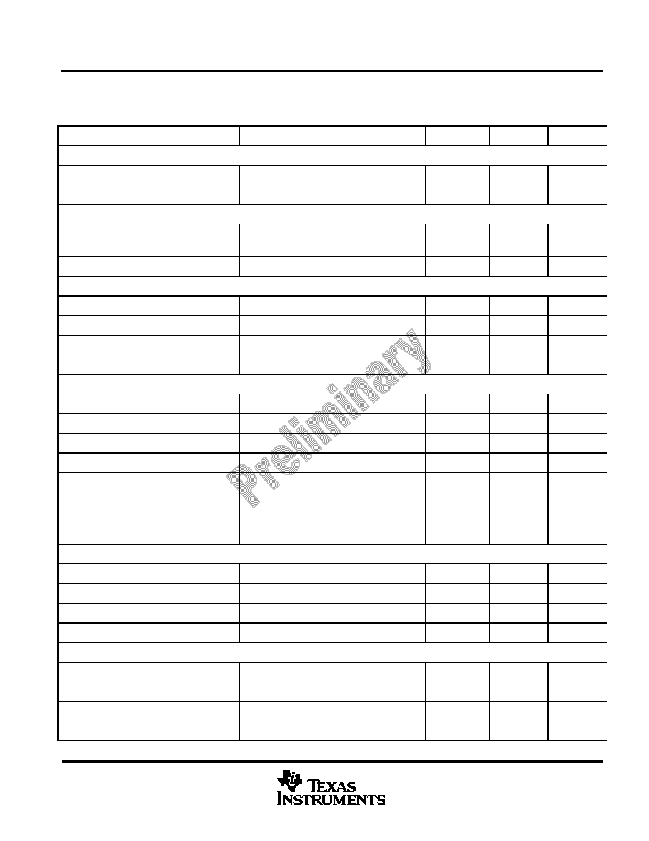
3 ELECTRICAL CHARACTERISTICS
VD33 = 3.3V, TA=-40 ∫C to 85 ∫C (unless otherwise noted)
PARAMETER CONDITIONS
MIN
TYP
MAX
UNIT
VDD Input Supply
VD33 supply voltage
3.14
3.3
3.46
V
ICC supply current
Normal operation
4
7
10
mA
VD25
Output voltage range
1uF ceramic connected,
without source current
2.4 2.45 2.5 V
Source current
1
5% maximum voltage drop
-10 mA
EAP & EAN
Input differential range
-0.2
2.5
V
Input bias current to EAP
VEAP-VEAN = 2.5V
-10
50
A
Output source current from EAN
-10
A
Bandwidth
2
MHz
PWM OUTPUT
Duty cycle
1
99
%
Rise time (t
r
)
1000pF cap load
15
ns
Fall time (t
f
)
1000pF cap load
15
ns
Dead band (t
db
)
Fs = 500KHz
20
512
ns
Fault shutdown delay (t
dl
)
The count of CLF is set
at zero
20 ns
PWM Frequency (F
sw
)
30
500
2000
KHz
Frequency set point Accuracy
T
A
= 25
∫C
5
%
ILIM
PWM Frequency (F
il
)
50
kHz
Duty cycle range
0
100
%
Fall time(t
f_il
)
1000pF cap load
15
ns
Rise time (t
f_il
)
1000pF cap load
15
ns
POWER GOOD
PGood assertion delay
TBD
s
PGood deassertion delay
TBD
s
Low level output voltage (V
OL
)
I PGood = 5 mA
0.4
V
High level output voltage (V
OH
)
I PGOOD = -5 mA
2.8
V

UCD9112
SEPEMBER 2006
9
www.ti.com
PMBus AERT
PMBus Alert assertion delay
TBD
s
PMBus Alert deassertion delay
TBD
s
Low level output voltage (V
OL
)
I alert = 5 mA
0.4
V
High level output voltage (V
OH
)
I alert = -5 mA
2.8
V
THERMAL SHUTDOWN
Shutdown temperature
Junction temperature
TBD
∫C
Hysteresis
TBD
∫C
I/O CHARACTERISTICS
High input voltage, V
IH
VD33=3.3V
2
3.45
V
Low input voltage, V
IL
VD33=3.3V
0.8
V
Input hysteresis voltage. VD33=3.3V 0.3
V
Output Voltage High (V
OH
)
VD33=3.3V, IOH = -5mA
2.8
Output Voltage Low (V
OL
)
VD33 = 3.3V, IOL = 5mA
0.4
PMBus/SMBus/I2C
FSMB PMBus/SMBus
operating frequency
Slave mode, SMBC 50%
duty cycle
100 kHz
FI2C I
2
C operating frequency
Slave mode, SCL 50%
duty cycle
400 kHz
t
(BUF)
Bus free time between
start and stop
4.7
us
t
(HD:STA)
Hold time after
(repeated) start
4.0
us
t
(SU:STA)
Repeated start setup
time
4.7
us
t
(SU:STO)
Stop setup time
4.0
us
t
(HD:DAT)
Data hold time
Receive Mode
0
ns
Transmit
Mode
300
ns
t
(SU:DAT)
Data setup time
250
ns
t
(TIMEOUT)
Error signal/detect
(1)
25 35 ms
t
(LOW)
Clock low period
4.7
us
t
(HIGH)
Clock high period
(2)
4.0 50 us
t
(LOW:SEXT)
Cumulative clock low
slave extend time
(3)
25
ms
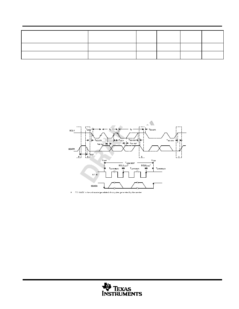
UCD9112
SEPTEMBER 2006
10
www.ti.com
t
(LOW:MEXT)
Cumulative clock low
master extend time
(4)
10
ms
t
f
Clock/data fall time
(5)
300 ns
t
r
Clock/data rise time
(6)
1000 ns
(1)
The UCD9112 times out when any clock low exceeds t
(TIMEOUT)
.
(2) t
(HIGH)
, Max, is the minimum bus idle time. SMBC = SMBD = 1 for t > 50 ms causes reset of any transaction involving
UCD9110 that is in progress. This specification is valid when the NC_SMB control bit remains in the default cleared state
(CLK[0]=0).
(3) t
(LOW:SEXT)
is the cumulative time a slave device is allowed to extend the clock cycles in one message from initial start to
the stop.
(4) t
(LOW:MEXT)
is the cumulative time a master device is allowed to extend the clock cycles in one message from initial start
to the stop.
(5) Fall time t
f
= 0.9VDD to (VILMAX ≠ 0.15)
(6) Rise time t
r
= VILMAX ≠ 0.15) to (VIHMIN + 0.15)
Figure 3-1. PMBus/SMBus/I2C Timing Diagram

UCD9112
SEPEMBER 2006
11
www.ti.com
4 TYPICAL CHARACTERISTICS
To be included in later revision of the data sheet
5 FUNCTION OVERVIEW
5.1 RESET
5.1.1 Power-on Reset
The UCD9112 has an integrated reset block which monitors the supply voltage. At power-up, the POR
detects the VD33 rise. When VD33 is greater than a predetermined reference point, VRST, a reset pulse is
generated and a startup delay sequence is initiated. At the end of the delay sequence, the system reset
signal is deasserted and the device begins normal operation. (See Table 5-1)
In applications with long VD33 rise times, the external reset (RST) should be used to ensure startup occurs
when the supply voltage is greater than the minimum operating voltage. At the normal operating condition,
this RST pin must be connected to a parallel combination of a 10k resistor and 0.1F capacitor to AVSS.
5.1.2 Brown-out Reset
The UCD9112 also has an integrated Brown-out Reset circuit that is used to generate a reset when the
supply voltage falls below a fixed trip reference voltage. The device is held in reset until the supply voltage
rises above the minimum voltage threshold, at which time a new reset pulse is generated and the POR circuit
restarts the device. (See Table 5-1)
5.1.3 Watchdog Timer
Built-in
Watchdog provide protection from unpredicted operation.
5.1.4 External Reset
The device can be forced into the reset state by an external circuit connected to the Pin RST. A logic high
voltage on this pin generates a reset signal. To avoid an erroneous trigger caused by the noise, a pull down
resistor and a decoupling cap is necessary.
Table 5-1 Device reset voltage threshold
VD33= 3.3V, TA= -40∫C to 85∫C (unless otherwise noted)
Parameter
Test Conditions
Min Typ Max
Unit
Power-on reset, VRST
2.4 2.5 2.8
V
Brown-out threshold
2.2
V
RST Delay
TBD
ms
Hysteresis
0.2
V

UCD9112
SEPTEMBER 2006
12
www.ti.com
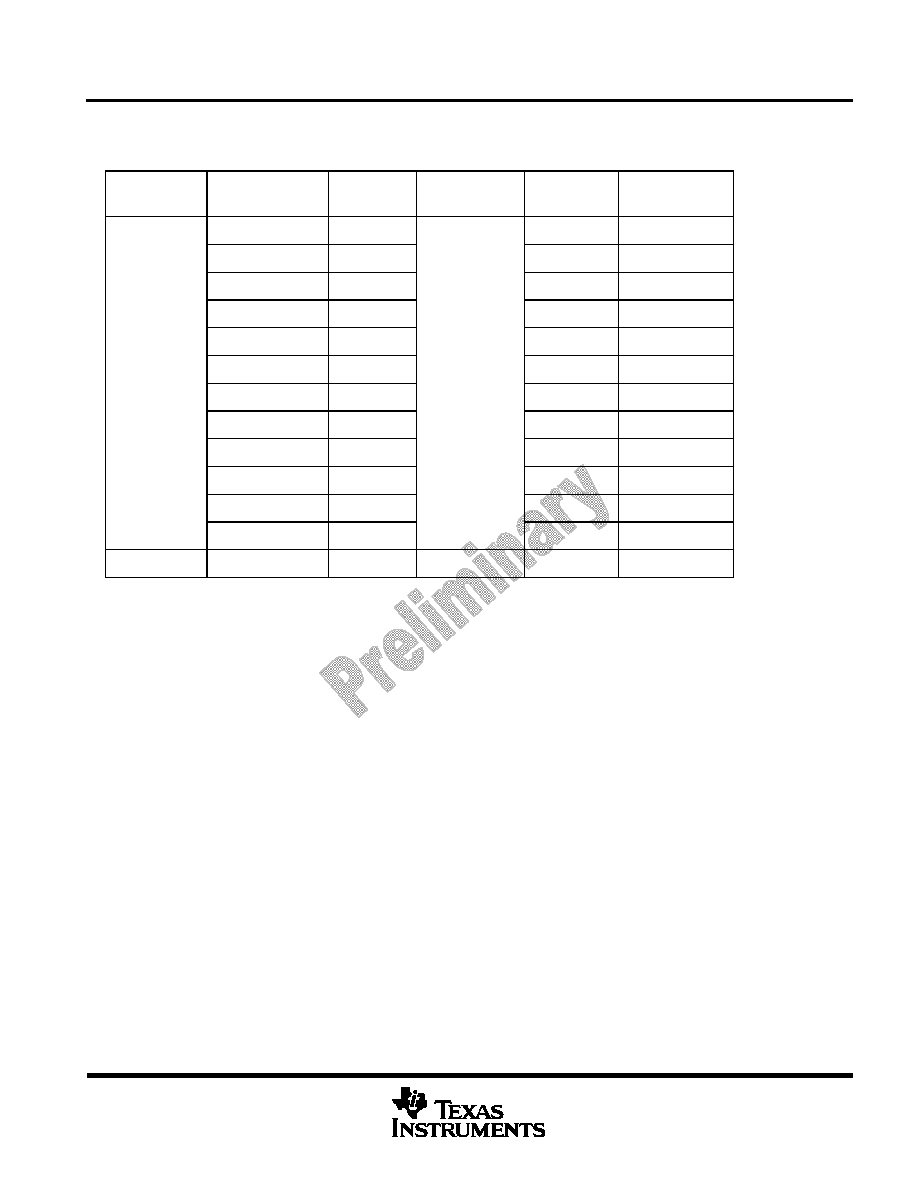
5.2 Analog Monitoring
The UCD9112 monitors 7 analog signals to determine supply operation. Table 5-2 below shows the analog
input pin assignments.
Table 5-2. Analog input assignment
Pin. No
Pin Name
Function Description
1
ADDR1
Address 1 voltage conversion
2
ADDR0
Address 0 voltage conversion
3
IOUT_0
Phase 0 output current conversion
4
VIN
POL input voltage conversion
5
VOUT
POL output voltage conversion
6
IOUT_1
Phase 1 output current conversion
Internal
-
Temperature sensing voltage conversion
The UCD9112 takes the proper action based on the information acquired from these analog inputs, for
example turning on the DC output or sending alarm signal to the host system if the output is under voltage.
The device temperature is monitored using an internal temperature sensor. The data can be reported to the
host after the UCD9112 receives the commands via PMBus. The PMBus commands will be addressed in the
section titled PMBus Interface.
5.2.1 Resolution
The external analog inputs have 3.22mV resolution based on a 3.3V VD33 input. The maximum input voltate
at the analog input should not exceed 3.0V for proper measurement.
In some applications, a voltage divider is used to reduce the voltage level applied to the analog input. The
division ratio changes the conversion resolution. .
5.2.2 Input Impedance
The input impedance is typically a 250 series input and a 30pF capacitor to ground. The inputs are
sampled and require 60ns of settling time. It is desirable to have a 0.1uF input capacitor at each analog
input pin.
UCD9112
SEPEMBER 2006
13
www.ti.com
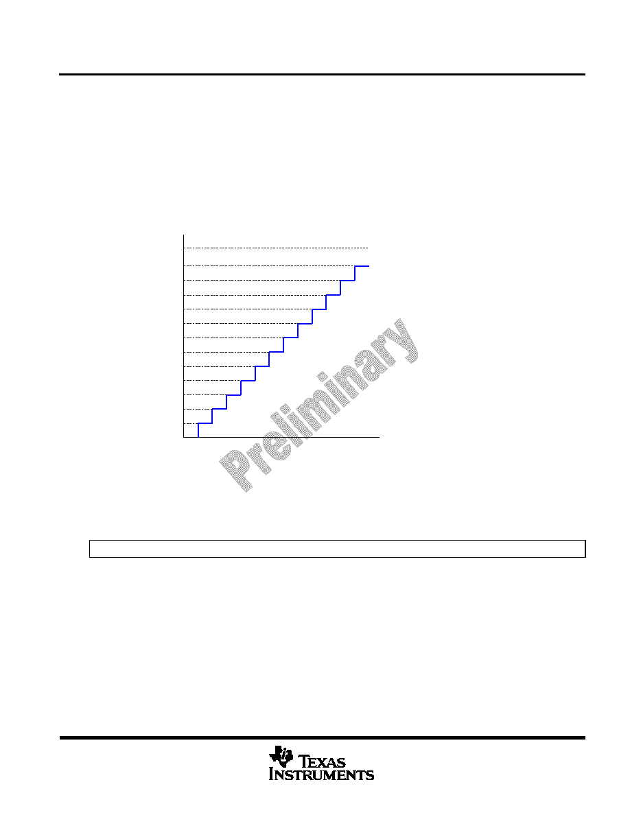
5.3 PMBus ADDRESS
The Digital POL system has the ability to be configured with different PMBus addresses. To configure
different addresses, a voltage will be applied to the pins ADDR1 and ADDR0 on the UCD9112.
The following table shows what PMBus addresses are indicated by the applied voltage.
Figure 5-1. V
addr
to PMBus address translation
Note that the nominal value for each voltage step (and each PMBus address) is in the center of each band.
The address can be represented by the formula:
PMBus_Addr = ADDR0 * 12 + ADDR1
Table 5-4 lists the examples of the PMBus address for given the voltage level on the pin1 and Pin2.
Addresses
0
1
2
3
4
5
6
7
8
9
10
11
V
ADDR
3.00
3.30
Address not valid 3.0< V
ADDR
< 3.3
0.25
0.50
0.75
1.00
1.25
1.50
1.75
2.00
2.25
2.50
2.75
UCD9112
SEPTEMBER 2006
14
www.ti.com
Table 5-4. The configuration of PMBus addresses
PMB_Addr0 PMB_Addr1
PBM
Address
PMB_Addr0 PMB_Addr
1
PBM Address
<0.25 0x00
<0.25
0x0C
0.25-0.5 0x01
0.25-0.5
0x0D
0.5-0.75 0x02
0.5-0.75
0x0E
0.75-1.0 0x03
0.75-1.0
0x0F
1.0-1.25 0x04
1.0-1.25
0x10
1.25-1.50 0x05
1.25-1.50
0x11
1.50-1.75 0x06
1.50-1.75
0x12
1.75-2.0 0x07
1.75-2.0
0x13
2.0-2.25 0x08
2.0-2.25
0x14
2.25-2.50 0x09
2.25-2.50
0x15
2.50-2.75 0x0A
2.50-2.75
0x16
<0.25
2.75-3.0 0x0B
0.25-0.50
2.75-3.0 0x17
The other address can be figured out by using the above formula. If the voltage placed on the address pins is
over 3.0V or below zero, the value is not valid.
5.4 PID COMPENSATOR
The PID compensator allows the output voltage to be regulated at the set point reference level with zero
steady state error and at the same time, maintain good dynamic performance. The high DC gain of the
control loop maintains the zero steady state error. This is realized by an integrator in the PID compensator.
However, the dynamic response may not be ideal if only an integrator exists in the control loop for different
applications. To further improve step response and stability, the PID compensator should be designed with
properly placed pole and zeros in order to achieve desired bandwidth and optimum phase margin, and gain
margin.
The synchronous buck topology is commonly used for non-isolated DC/DC converters. The placement of the
pole and zeros is determined by the output filter inductor, capacitor and the ESR parasitic. In the traditional
power supply design, an operational error amplifier and external compensation components are used to
implement the pole and zeros. Using the UCD9112, the output voltage is properly scaled and fed to the
UCD9112 error converter. The ADC output is then fed to the UCD9112's on chip PID compensator. The
compensator is configured using the graphical user interface (during development) and the configuration is
stored into the UCD9112's flash memory.
5.5 OUTPUT VOLTAGE SENSING

UCD9112
SEPEMBER 2006
15
www.ti.com
Figure 5-2. Output voltage sensing circuitry
Figure 5-2 shows the voltage sensing circuitry in UCD9112. It is part of feedback loop. Two dedicated pins,
EAP and EAN, are employed to sense the output voltage differentially. The differential sensing can
effectively reduce the noise induced by the switching devices. The maximum voltage for VEAP-VEAN
should be less than 2.45V. If output voltage is higher than 2.45V, a voltage divider should be used to
decrease the input voltage level below 2.45V.

UCD9112
SEPTEMBER 2006
16
www.ti.com
6 PMBus INTERFACE
PMBus is an industry standard specification for power management.. The UCD9112 supports all of the
PMBus data commands that are relevant to this application. Most of the functionality in the DPOL application
for the UCD9112 uses PMBus commands to support each of the functions. For each PMBus command
supported in this specification, all SMBus transaction types associated with that command are also
supported. This enables the user to write and read the support parameters through the PMBus commands,
and SMBus transactions.
The UCD9112 is PMBus compliant, in accordance with the "Compliance" section of the PMBus specification.
The firmware is also compliant with the SMBus 1.1 specification, including support for the SMBus ALERT
function.
6.1 PMBus TIMING
The timing characteristics and timing diagram for the communications interface that supports I
2
C, SMBus and
PMBus is shown at Figure 3 in the section electrical characteristics.
6.2 OUTPUT CONFIGURATION COMMANDS
6.2.1 Remote ON/OFF
Remote on/off is supported by the software in the UCD9112 controller. This behavior is configurable and is
supported by a combination of the PMBus commands below and the PMB_CTL signal which is connected to
Pin 23.
The PMBus commands that support this functionality are:
ON_OFF_CONFIG
OPERATION
The ON_OFF_CONFIG command is used to configure the policy by which the unit is turned on and off, and
the OPERATION command is used to turn the unit on and off according to this policy.
Power supply is turned on when PMB_CTL pin is pulled high; it is turned off when the pin is pulled down.
6.2.1 Output Voltage Set Point
The PMBus commands that support this functionality are:
VOUT_MODE
VOUT_COMMAND
VOUT_MAX
VOLTAGE_SCALE_LOOP
VOLTAGE_SCALE_MONITOR

UCD9112
SEPEMBER 2006
17
www.ti.com
VOUT_MODE and VOUT_COMMAND set the new output voltage mode and the VOUT_MAX command sets
the maximum output voltage. VOUT_MODE is used for commanding and reading output voltage, and it
consists of a three-bit mode and a five-bit parameter representing the exponent used in output voltage
Read/Write. The voltage set by VOUT_COMMAND is more than VOUT_MAX, the command is ignored.
The VOLTAGE_SCALE_LOOP and VOLTAGE_SCALE_MONITOR commands are used to scaling the
output voltage.
6.2.3 Output Voltage Calibration
The UCD9112 supports V
out
output calibration. Output calibration is supported dynamically and can be
changed with the supply is operational. The PMBus command that supports this functionality is:
VOUT_CAL
The VOUT_CAL command supports output voltage calibration by providing a fixed offset voltage to the
output voltage command values.
6.2.4 Margin up/down
The UCD9112 supports margin up/down linearly through a programmable rate. The PMBus commands to
support this functionality are:
VOUT_MARGIN_HIGH
VOUT_MARGIN_LOW
VOUT_TRANSITION_RATE
The VOUT_MARGIN_HIGH command is used to provide the unit with the voltage to which the output is to be
changed when the operation is set to "margin high". The VOUT_MARGIN_LOW command is used to provide
the unit with the voltage to which the output is to be changed when the operation is set to "margin low".
When margining up or down, the rate at which the voltage margining increases or decreases will be specified
by the VOUT_TRANSITION_RATE command.
6.2.5 Output Current Measurement
There are two commands in UCD9112 to measure output current. The output current is measured by sensing
the voltage drop across the DCR of each output inductor. The current of each phase is added to provide the
IOUT value. The PMBus commands that support this functionality are:
IOUT_SCALE
IOUT_CAL_OFFSET
The UCD9112 has two manufacturer specific commands to report the current on each of the two phases.
The IOUT_CAL_OFFSET command support output current calibration by nullifying any offsets in the current
sensing circuits. The IOUT_SCALE command is used to set the ratio of the voltage at the current sense pins
to the sensed current of each phase.
The output current can be calculated as:
UCD9112
SEPTEMBER 2006
18
www.ti.com
OFFSET
CAL
IOUT
SCALE
IOUT
V
I
SENSE
o
-
-
-
-
=
This can be graphically depicted as shown below.
Figure 6-1. Current Gain and Offset
6.2.6 Start up into Pre-Bias
The UCD9112 supports starting the power supply when there is an existing output voltage when the system
starts. The system will start up with an output voltage higher than the output voltage set point.
The duty cycle is calculated by dividing V
out
by V
in
(duty cycle = V
out
/ V
in
). The time constant for this operation
is 50 ms and regulation will be achieved by this time.
When the PMBus CONTROL line is asserted, the UCD9112 looks at the output voltage to determine if a
prebias is present. The algorithm for this is as follows:
If V
out
< 300 mV, then the startup is done assuming no pre-bias. Start up proceeds normally through delay
and soft start states.
If V
out
> 3.65V, then the device does not attempt startup
If V
out
> output voltage set point, then disable Overvoltage Protection (OVP), calculate the duty cycle (V
out
/
V
in
), bypass the soft start state and commence switching. When V
out
< V
out_
high limit, re-enabled OVP.
The response time from this action will be less than 10 ms.
If V
out
< output voltage set point, then turn off V
out
low protection, calculate the duty cycle, bypass the soft
start state and commence switching. When V
out
> V
out
low, then re-enable V
out
low protection.
There are no PMBus commands associated with this functionality.
6.2.7 Output Voltage Sequencing
The UCD9112 supports output voltage sequencing. Output voltage sequencing is started based on receiving
an indication from the PMB CONTROL (PMB_CTL) signal from the system host.
The PMBus commands that support this functionality are:
I
OUT
V
SENSE
Offset
Gain
Measured
value
Adjusted
value

UCD9112
SEPEMBER 2006
19
www.ti.com
TON_DELAY
TOFF_DELAY
TON_DELAY is used to specify the delay from when the PMBus CONTROL line is asserted to when the
output voltage starts to rise. TOFF_DELAY is used to specify the delay from when the PMBus CONTROL
line is deasserted to when the output voltage starts to fall.
6.2.8 Output Voltage Soft Start
Soft start timing starts when the PMB_CTL line is asserted (voltage rise). The system configures the delay
from the assertion of the PMB_CTL signal to when the output voltage entered the regulation band. The
system also configures the maximum time this process can take, without causing an undervoltage fault, and
what action to take for an error.
The PMBus commands that support this functionality are:
TON_RISE
TON_MAX_FAULT_LIMIT
TON_MAX_FAULT_RESPONSE
When the voltage is rising, the TON_RISE command specifies the time from when output voltage tracking
starts, to when the output voltage enters the regulation band. The TON_MAX_FAULT_LIMIT command
specifies the maximum amount of time that this process can take, before an undervoltage fault will occur.
The TON_MAX_FAULT_RESPONSE command specifies the action to be taken if the power supply does not
reach the regulation band before the maximum time specified by TON_RISE has elapsed.
6.2.9 Output Voltage Soft Stop
Soft stop timing starts when the PMB_CTL line is deasserted (voltage fall).
TOFF_FALL
TOFF_MAX_FAULT_LIMIT
TOFF_MAX_FAULT_RESPONSE
The TOFF_FALL command specifies the time from when the voltage starts to fall to when it is off. The
TOFF_MAX_FAULT_LIMIT command specifies the maximum amount of time that this process can take,
before an overvoltage fault will occur. The TOFF_MAX_FAULT_RESPONSE command specifies the action
to be taken if the power supply does not reach 0V by the maximum time specifies in TOFF FALL has
elapsed.
In the event that the voltage fails to rise or fall according to the criteria above, the STATUS_VOUT command
will reflect the failure to meet the configured output voltage tracking.

UCD9112
SEPTEMBER 2006
20
www.ti.com
6.2.10
Power Good (PGOOD)
The UCD9112 supports an indication of power good to the host. The UCD9112 will monitor output voltage
and will either assert or de-assert the power good signal based on this voltage. The UCD9112 uses the
PGOOD (Pin 21) as the power good signal and the polarity of this signal can be configured as active high or
active low through PMBus. This signal drives an open collector GPIO pin on the host system.
Power good is asserted when the system is operational and is delivering the configured output voltage.
Power good will be de-asserted when any condition (fault or otherwise) causes the system to ramp down
output voltage. The system will assert (or de-assert) this signal within 1ms of the event that causes the
transition.
The PMBus commands that support this functionality are:
POWER_GOOD_ON
POWER_GOOD_OFF
MFR_SPECIFIC_00
The POWER_GOOD_ON command is used to specify the voltage at which the Power Good signal should be
asserted. The POWER_GOOD_OFF command is used to specify the voltage at which the Power Good
signal should be de-asserted. The MFR_SPECIFIC_00 command configures the polarity of the Power Good
signal. A value of 0 in the least significant byte in this command means that the power good signal should be
configured to be active low. A value of 1 in the least significant byte in this command means that the power
good signal should be configured to be active high.
6.3 PROTECTION COMMANDS
UCD9112 provides many features to monitor input voltage, output voltage, output current, and temperature.
The thresholds can be programmable through PMBus, and the status and the faults are sent to the host
computer if requested.
6.3.1 Input Under Voltage Protection(VIN_UVP)
Input voltage is sensed on VIN (Pin4) of UCD9112, and the data is processed based on the threshold
programmed through PMBus. The PMBus commands that will support this functionality are:
VIN_UV_WARN_LIMIT
VIN_UV_FAULT_LIMIT
VIN_UV_FAULT_RESPONSE
VIN_ON
VIN_OFF
When the input voltage starts to rise towards the regulation band, the VIN_ON command sets the voltage at
which power conversion starts. When the voltage is in the regulation band, the system then observes the

UCD9112
SEPEMBER 2006
21
www.ti.com
input voltage for both input under and over voltage warnings and faults. If the voltage falls below the value
set by the VIN_OFF command, then power conversion will stop.
If the voltage falls below the value set through the VIN_UV_WARN_LIMIT command, then an under voltage
warning occurs.
If the voltage continues to fall and falls below the value set through the VIN_UV_FAULT_LIMIT command,
then an under voltage fault occurs. The action taken in this event is specified by the
VIN_UV_FAULT_RESPONSE command.
When an under-voltage fault occurs, the VIN_UV_FAULT_RESPONSE register instructs the system how to
react. There are two response bits that instruct the system what to do in the event of these failures. Input
Under-voltage Fault Response Actions
6.3.2 Input Over Voltage Protection (VIN_OVP)
The UCD9112 supports warnings and faults for input over voltage protection. The latency from when the
voltage goes out of range to when power is ramped down is 20ms.
The PMBus commands that support this functionality are:
VIN_OV_WARN_LIMIT
VIN_OV_FAULT_LIMIT
VIN_OV_FAULT_RESPONSE
For input over voltage
warnings
, the VIN_OV_WARN_LIMIT command is used to set the input voltage at
which an over voltage warning occurs.
6.3.3 Output Over Voltage Protection (VO_OVP)
UCD9112 monitors output voltage by the VOUT (Pin5). In order to compensate for possible transient cases,
when the first over-voltage reading happens, the firmware will monitor the output voltage more closely. If a
second over-voltage reading happens within 100
s, the firmware will flag this as an over-voltage event and
not just as a transient condition.
When an over-voltage fault event occurs, the firmware will send out a short PWM pulse and toggle the SRE
signal to latch the sync FET on. This will make sure that the driver will try to pull down the over voltage
actively through the sync FET.
The UCD9112 offers programmable output over voltage protection. The firmware can be configured to
monitor (and act upon) OVP faults and warnings independently. If this condition occurs, the UCD9112 will
take the action configured through the PMBus RESPONSE commands shown below.
The PMBus commands that support this functionality are:
VOUT_OV_WARN_LIMIT
VOUT_OV_FAULT_LIMIT
VOUT_OV_FAULT_RESPONSE

UCD9112
SEPTEMBER 2006
22
www.ti.com
For output under voltage
warnings
, the VOUT_OV_WARN_LIMIT command sets the voltage at which an
output under voltage warning will occur.
For output under voltage
faults
, the VOUT_UV_FAULT_LIMIT command sets the voltage at which an output
under voltage fault will occur. In this event, the VOUT_UV_FAULT_RESPONSE command specifies the
action to be taken.
When an OVP fault occurs, the Vout_OV_FAULT_RESPONSE register instructs the system how to react.
There are two response bits that instruct the system what to do in the event of these failures.
6.3.4 Output Under Voltage Protection (VO_UVP)
When a fault condition is detected, the PMBus ALERT signal is asserted to the host controller to announce
this event. The latency between the under voltage fault event and the PMBus ALERT to the host is 1 ms.
After this event has occurred, the system reacts according to the configuration according to the RESPONSE
commands below. The latency between the under voltage fault event happening and the UCD9112 taking
the configured action is 10 ms.
The output under voltage warning does not raise the PMBus ALERT signal. The latency between when
output under voltage warning threshold being crossed and the UCD9112 taking the configured action is 10
ms.
The PMBus commands that support this functionality are:
VOUT_UV_WARN_LIMIT
VOUT_UV_FAULT_LIMIT
VOUT_UV_FAULT_RESPONSE
For output under voltage
warnings
, the VOUT_UV_WARN_LIMIT command specifies the value of the output
voltage that will cause an under voltage warning.
For output under voltage
faults
, the VOUT_UV_FAULT_LIMIT command specifies the value of the output
voltage that will cause an under voltage fault. The VOUT_UV_FAULT_RESPONSE command will specify the
action to be taken should this event occur.
When an output under voltage fault occurs, the VOUT_UV_FAULT_RESPONSE register instructs the system
how to react. There are two response bits that instruct the system what to do in the event of these failures.
6.3.5 Output Over Current Protection (IO_OCP)
The UCD9112 cooperated with the UCD7230 drive monitors the output current and provides output current
protection. Current is sensed either by the top FET's RDSON or by DCR of the output inductor. There are
two different sensing methods and two different protections.
First, by sensing the current of top MOSFET, the cycle-by-cycle current is obtained on UCD7230. The peak
current is compared to the peak current threshold set by external resistors. If the peak current of top FET is
higher than the set point, the gate drive pulse is cut off, and the top FET is immediately turned off. In the
event the output is short and the current increases extremely fast, this pulse-by-pulse protection can take
actions immediately to avoid the damage of the power converter. When over current happens, the output of
CLF is set and kept high until the next switching cycle. The UCD9112 counts the number of CLF low to high
transitions. If over current continues for multiple switching cycles greater than the limit set in the UCD9112,

UCD9112
SEPEMBER 2006
23
www.ti.com
the decision will be made by UCD9112 to shut off the DPWM outputs. The converter is going to enter hiccup
mode or latched-off mode.
Second, the output current is also obtained by measuring the voltage across the DCR of each output
inductor. By properly selecting RC network that is connected in parallel with the output inductor, the output
inductor current is sensed and fed to the UCD7230. The UCD9112 provides current limit (I
LIM
) threshold to
the UCD7230 through a filtered PWM output. The sensed voltage across the DCR of each output inductor is
compared to I
LIM
using a high speed comparator in the UCD7230. If the ICS > I
LIM
, the CLF is set. The
UCD9112 counts the number of CLF high to low transitions. The converter enters hiccup or latched-off mode
after the number of CLF pulses is more than the limit set in the UCD9112. The current limit threshold I
LIM
and
the number of CLF pulses are programmable through PMBus.
The PMBus commands that support this functionality are:
IOUT_OC_WARN_LIMIT
IOUT_OC_FAULT_LIMIT
IOUT_OC_FAULT_RESPONSE
MFR_SPECIFIC_01
For over current warnings, the IOUT_OC_WARN_LIMIT command specifies the current at which the over
current warning occurs.
For over current faults, the IOUT_OC_FAULT_LIMIT command specifies the current at which the over
current fault occurs. When this event occurs, the IOUT_OC_FAULT_RESPONSE command specifies the
action to be taken by the system.
The number of current limit flags to accept before taking action can be configured by using the
MFR_SPECIFIC_01 command. The 16b data value from this command will represent the number of CLF
events.
The inductor current of phase0 and phase1 are amplified in the UCD7230. Then, the current of each phase is
input to UCD9112 on the IOUT_0 and IOUT_1. The software will monitor the output current and send
warning signal if the current is over limit.
6.3.6 Over Temperature Protection (OTP)
The UCD9112 supports over temperature protection warnings and faults. There is a temperature sensor in
the UCD9112 that is used for sensing over temperature events. The temperature sensor is calibrated
according to a calculation based on current output and the power scale using a manufacturer specific
command. The latency between over temperature events and system reaction time is 20ms.
The PMBus commands to support this functionality are:
OT_WARN_LIMIT
OT_FAULT_LIMIT
OT_FAULT_RESPONSE
MFR_SPECIFIC_02

UCD9112
SEPTEMBER 2006
24
www.ti.com
For over temperature warnings, the OT_WARN_LIMIT command specifies the temperature at which the
power supply will indicate an over temperature warning alarm.
For over temperature faults, the OT_FAULT_LIMIT command specifies the temperature at which the power
supply will indicate a fault. The OT_FAULT_RESPONSE command specifies the action to be taken in the
event of a temperature fault condition in the power supply.
The MFR_SPECIFIC_02 command will be used to calibrate the temperature reported by the temperature
sensor on the UCD9112.
When an over-temperature fault occurs, the OT_FAULT_RESPONSE register instructs the system how to
react. There are two response bits that instruct the system what to do in the event of these failures.
6.4 STATUS & FAULT REPORTING COMMANDS
The UCD9112 controller supports status and fault reporting, for maintenance of an operating supply. The
PMBus commands are listed below:
STATUS_BYTE
STATUS_WORD
STATUS_VOUT
STATUS_IOUT
STATUS_INPUT
STATUS_TEMPERATURE
STATUS_CML
CLEAR_FAULTS
STATUS_BYTE command returns one byte of information with a summary of the most critical faults.
STATUS_WORD command returns two bytes of information with a summary of the unit fault condition.
STATUS_VOUT command returns one byte information of output voltage
STATUS_IOUT command returns one byte information of output current
STATUS_INPUT command returns one byte information of input voltage
STATUS_TEMPERARUE command returns one byte information of temperature
CLEAR_FAULT command clears any set faults
6.5 NON-VOLATILE STORAGE COMMANDS
The UCD9112 supports storing configuration valued to it's non-volatile memory. The latency for this
operation is 1 second. The PMBus commands that support this functionality are:
STORE_DEFAULT_ALL
RESTORE_DEFAULT_ALL

UCD9112
SEPEMBER 2006
25
www.ti.com
STORE_DEFAULT_CODE
RESTORE_DEFAULT_CODE
STORE_USER_ALL
RESTORE_USER_ALL
STORE_USER_CODE
RESTORE_USER_CODE
The STORE_DEFAULT_ALL command stores all default values in the system to non-volatile memory. The
RESTORE_DEFAULT_ALL command will set all operational values to the values stored in non-volatile
memory.
The STORE_DEFAULT_CODE command will store the given value for the given command to non-volatile
memory. The RESTORE_DEFAULT_CODE restore the given value for the given command to operational
memory from non-volatile memory.
The STORE_USER_ALL command stores all user values in the system to non-volatile memory. The
RESTORE_USER_ALL command will restore all user values from non-volatile memory to operational
memory.
The STORE_USER_CODE command will store the given value for the given user command to non-volatile
memory. The RESTORE_USER_CODE will restore the given value for the given command from non-volatile
memory to operational memory.
6.5 HOST DATA STORAGE COMMANDS
The PMBus commands to support this functionality are:
MFR_ID
MFR_MODEL
MFR_REVISION
MFR_DATE
MFR_SERIAL
The MFR_ID, MFR_MODEL, MFR_REVISION, MFR_DATE and MFR_SERIAL commands will be used by
the firmware to store that appropriate data from the release of the UCD9112 and driver, as well as firmware
for the application.
7 DUAL PHASE CURRENT BALANCING
UCD9112 uses two pins, Pin Iout_0 and Iout_1, to sense the output current of each phase. The current
accuracy is important because the current values are used for current balance. DCR of output inductor varies
with temperature and is compensated for temperature changes by the UCD9112. An assumption that is

UCD9112
SEPTEMBER 2006
26
www.ti.com
made is that the internal temperature of the device is equivalent to the temperature of each inductor. The
current balancing is implemented through the software. The current balancing condition is reported to the
host. The below requirement of current balancing can be met for UCD9112 dual phase application.
Table 7-1. Current balancing of two phases
Test condition at 25C.
Output Total Current
Two Phase Current Difference
0% to 30%, 0A to 12A
TBD
30% to 50%, 12A to 20A
TBD
50% to 100%, 20A to 40A
TBD
8 GUI
UCD9112 provides GUI (Graphic User Interface) for the user to configure POL operating condition. The
functionality of GUI supporting UCD9112 is based on the PMBus specifications compliance. The key
functions of GUI are listed below:
- PID coefficients programming
- POL ON/OFF
- Vout set point
- Converter switching frequency set
- Output voltage soft start and soft stop
- Read output voltage
- Read output current
- Read input voltage
- Read temperature
- Fault threshold configuration
- Manufacturing information storage
More information is provided on the GUI User's Manual. Figure 6 is the front picture of GUI shown before
users.
UCD9112
SEPEMBER 2006
27
www.ti.com
Figure 8-1. Example GUI Interface for POL Configuration
UCD9112
SEPTEMBER 2006
28
www.ti.com
Figure 8-2. Example GUI Design Tool
9 PACKAGE INFORMATION
The UCD9112 is available in Texas Instruments' 32-pin PowerPAD
TM
plastic quad flatpack package.
Figure 9-1. 32-Pin PowerPAD
TM
QFN Package

UCD9112
SEPEMBER 2006
29
www.ti.com