TMS320F2809, TMS320F2808, TMS320F2806
TMS320F2802, TMS320F2801, UCD9501
TMS320C2802, TMS320C2801 Digital Signal Processors
Data Manual
Literature Number: SPRS230G
October 2003 ≠ Revised February 2006
UNLESS
OTHERWISE
NOTED
this
document
contains
PRODUCTION DATA information current as of publication date.
Products conform to specifications per the terms of Texas
Instruments standard warranty. Production processing does not
necessarily include testing of all parameters.

www.ti.com
Contents
TMS320F2809, TMS320F2808, TMS320F2806
TMS320F2802, TMS320F2801, UCD9501
TMS320C2802, TMS320C2801 Digital Signal Processors
SPRS230G ≠ OCTOBER 2003 ≠ REVISED FEBRUARY 2006
Revision History
...........................................................................................................................
9
1
F280x, C280x, UCD9501 DSPs
..............................................................................................
11
1.1
Features
.....................................................................................................................
11
1.2
Trademarks
.................................................................................................................
12
2
Introduction
.......................................................................................................................
13
2.1
Pin Assignments
............................................................................................................
15
2.2
Signal Descriptions
.........................................................................................................
19
3
Functional Overview
...........................................................................................................
25
3.1
Memory Map
................................................................................................................
26
3.2
Brief Descriptions
...........................................................................................................
32
3.2.1
C28x CPU
.......................................................................................................
32
3.2.2
Memory Bus (Harvard Bus Architecture)
....................................................................
32
3.2.3
Peripheral Bus
..................................................................................................
33
3.2.4
Real-Time JTAG and Analysis
................................................................................
33
3.2.5
Flash
..............................................................................................................
33
3.2.6
ROM
...............................................................................................................
33
3.2.7
M0, M1 SARAMs
...............................................................................................
34
3.2.8
L0, L1, H0 SARAMs
............................................................................................
34
3.2.9
Boot ROM
........................................................................................................
34
3.2.10
Security
..........................................................................................................
35
3.2.11
Peripheral Interrupt Expansion (PIE) Block
..................................................................
36
3.2.12
External Interrupts (XINT1, XINT2, XNMI)
...................................................................
36
3.2.13
Oscillator and PLL
..............................................................................................
36
3.2.14
Watchdog
........................................................................................................
36
3.2.15
Peripheral Clocking
.............................................................................................
36
3.2.16
Low-Power Modes
..............................................................................................
36
3.2.17
Peripheral Frames 0, 1, 2 (PFn)
..............................................................................
37
3.2.18
General-Purpose Input/Output (GPIO) Multiplexer
.........................................................
37
3.2.19
32-Bit CPU-Timers (0, 1, 2)
...................................................................................
37
3.2.20
Control Peripherals
.............................................................................................
37
3.2.21
Serial Port Peripherals
.........................................................................................
38
3.3
Register Map
................................................................................................................
38
3.4
Device Emulation Registers
...............................................................................................
41
3.5
Interrupts
....................................................................................................................
42
3.5.1
External Interrupts
..............................................................................................
44
3.6
System Control
.............................................................................................................
45
3.6.1
OSC and PLL Block
............................................................................................
47
3.6.2
Watchdog Block
.................................................................................................
49
3.7
Low-Power Modes Block
..................................................................................................
51
4
Peripherals
........................................................................................................................
52
4.1
32-Bit CPU-Timers 0/1/2
..................................................................................................
52
4.2
Enhanced PWM Modules (ePWM1/2/3/4/5/6)
..........................................................................
54
4.3
Hi-Resolution PWM (HRPWM)
...........................................................................................
56
4.4
Enhanced CAP Modules (eCAP1/2/3/4)
................................................................................
57
4.5
Enhanced QEP Modules (eQEP1/2)
.....................................................................................
59
4.6
Enhanced Analog-to-Digital Converter (ADC) Module
................................................................
61
4.7
Enhanced Controller Area Network (eCAN) Modules (eCAN-A and eCAN-B)
.....................................
66
4.8
Serial Communications Interface (SCI) Modules (SCI-A, SCI-B)
....................................................
71
4.9
Serial Peripheral Interface (SPI) Modules (SPI-A, SPI-B, SPI-C, SPI-D)
...........................................
74
4.10
Inter-Integrated Circuit (I
2
C)
...............................................................................................
78
2
Contents

www.ti.com
TMS320F2809, TMS320F2808, TMS320F2806
TMS320F2802, TMS320F2801, UCD9501
TMS320C2802, TMS320C2801 Digital Signal Processors
SPRS230G ≠ OCTOBER 2003 ≠ REVISED FEBRUARY 2006
4.11
GPIO MUX
..................................................................................................................
80
5
Device Support
..................................................................................................................
84
5.1
Device and Development Support Tool Nomenclature
................................................................
84
5.2
Documentation Support
...................................................................................................
86
6
Electrical Specifications
......................................................................................................
88
6.1
Absolute Maximum Ratings
...............................................................................................
88
6.2
Recommended Operating Conditions
...................................................................................
89
6.3
Electrical Characteristics
.................................................................................................
89
6.4
Current Consumption
.....................................................................................................
90
6.4.1
Reducing Current Consumption
..............................................................................
94
6.4.2
Current Consumption Graphs
..................................................................................
95
6.5
Timing Parameter Symbology
............................................................................................
96
6.5.1
General Notes on Timing Parameters
........................................................................
96
6.5.2
Test Load Circuit
................................................................................................
97
6.5.3
Device Clock Table
.............................................................................................
97
6.6
Clock Requirements and Characteristics
...............................................................................
98
6.7
Power Sequencing
.........................................................................................................
99
6.7.1
Power Management and Supervisory Circuit Solutions
....................................................
99
6.8
General-Purpose Input/Output (GPIO)
.................................................................................
102
6.8.1
GPIO - Output Timing
.........................................................................................
102
6.8.2
GPIO - Input Timing
...........................................................................................
103
6.9
Enhanced Control Peripherals
..........................................................................................
108
6.9.1
Enhanced Pulse Width Modulator (ePWM) Timing
........................................................
108
6.9.3
External Interrupt Timing
.................................................................................................
110
6.9.4
I
2
C Electrical Specification and Timing
................................................................................
111
6.9.5
Serial Peripheral Interface (SPI) Master Mode Timing
..............................................................
111
6.9.6
SPI Slave Mode Timing
..................................................................................................
115
6.9.7
On-Chip Analog-to-Digital Converter
...................................................................................
118
6.9.7.1
ADC Power-Up Control Bit Timing
..........................................................................
119
6.9.7.2
Definitions
......................................................................................................
120
6.9.7.3
Sequential Sampling Mode (Single-Channel) (SMODE = 0)
............................................
121
6.9.7.4
Simultaneous Sampling Mode (Dual-Channel) (SMODE = 1)
...........................................
122
6.10
Detailed Descriptions
....................................................................................................
123
6.11
Flash Timing
...............................................................................................................
124
6.12
ROM Timing
...............................................................................................................
125
7
Migrating From F280x Devices to C280x Devices
..................................................................
126
7.1
Migration Issues
...........................................................................................................
126
8
Mechanical Data
...............................................................................................................
127
Contents
3

www.ti.com
TMS320F2809, TMS320F2808, TMS320F2806
TMS320F2802, TMS320F2801, UCD9501
TMS320C2802, TMS320C2801 Digital Signal Processors
SPRS230G ≠ OCTOBER 2003 ≠ REVISED FEBRUARY 2006
List of Figures
2-1
TMS320F2808 100-Pin PZ LQFP (Top View)
.................................................................................
15
2-2
TMS320F2806 100-Pin PZ LQFP (Top View)
.................................................................................
16
2-3
TMS320F2802, TMS320F2801/UCD9501, TMS320C2802, TMS320C2801 100-Pin PZ LQFP
(Top View)
.........................................................................................................................
17
2-4
TMS320F2808, TMS320F2806,TMS320F2802, TMS320F2801,
TMS320C2802, TMS320C2801 100-Ball GGM and ZGM MicroStar BGATM (Bottom View)
...........................
18
3-1
Functional Block Diagram
........................................................................................................
25
3-2
F2808 Memory Map
..............................................................................................................
26
3-3
F2806 Memory Map
..............................................................................................................
27
3-4
F2802, C2802 Memory Map
.....................................................................................................
28
3-5
F2801/9501, C2801 Memory Map
..............................................................................................
29
3-6
External and PIE Interrupt Sources
.............................................................................................
42
3-7
Multiplexing of Interrupts Using the PIE Block
................................................................................
43
3-8
Clock and Reset Domains
.......................................................................................................
45
3-9
OSC and PLL Block Diagram
...................................................................................................
47
3-10
Using a 3.3-V External Oscillator
...............................................................................................
47
3-11
Using a 1.8-V External Oscillator
...............................................................................................
47
3-12
Using the Internal Oscillator
.....................................................................................................
47
3-13
Watchdog Module
.................................................................................................................
50
4-1
CPU-Timers
........................................................................................................................
52
4-2
CPU-Timer Interrupt Signals and Output Signal
..............................................................................
53
4-3
Multiple PWM Modules in a 280x System
.....................................................................................
54
4-4
ePWM Sub-Modules Showing Critical Internal Signal Interconnections
...................................................
56
4-5
eCAP Functional Block Diagram
................................................................................................
57
4-6
eQEP Functional Block Diagram
................................................................................................
59
4-7
Block Diagram of the ADC Module
.............................................................................................
62
4-8
ADC Pin Connections With Internal Reference
...............................................................................
63
4-9
ADC Pin Connections With External Reference
..............................................................................
64
4-10
eCAN Block Diagram and Interface Circuit
....................................................................................
67
4-11
eCAN-A Memory Map
............................................................................................................
68
4-12
eCAN-B Memory Map
............................................................................................................
69
4-13
Serial Communications Interface (SCI) Module Block Diagram
............................................................
73
4-14
SPI Module Block Diagram (Slave Mode)
.....................................................................................
77
4-15
I
2
C Peripheral Module Interfaces
...............................................................................................
79
4-16
GPIO MUX Block Diagram
.......................................................................................................
80
4-17
Qualification Using Sampling Window
..........................................................................................
83
5-1
Example of TMS320x280x Device Nomenclature
............................................................................
85
5-2
Example of UCD Device Nomenclature
........................................................................................
85
6-1
Typical Operational Current Versus Frequency (F2808)
....................................................................
95
6-2
Typical Operational Power Versus Frequency (F2808)
......................................................................
95
4
List of Figures

www.ti.com
TMS320F2809, TMS320F2808, TMS320F2806
TMS320F2802, TMS320F2801, UCD9501
TMS320C2802, TMS320C2801 Digital Signal Processors
SPRS230G ≠ OCTOBER 2003 ≠ REVISED FEBRUARY 2006
6-3
3.3-V Test Load Circuit
...........................................................................................................
97
6-4
Clock Timing
.......................................................................................................................
99
6-5
Power-on Reset
..................................................................................................................
100
6-6
Warm Reset
......................................................................................................................
101
6-7
Example of Effect of Writing Into PLLCR Register
..........................................................................
102
6-8
General-Purpose Output Timing
...............................................................................................
102
6-9
Sampling Mode
..................................................................................................................
103
6-10
General-Purpose Input Timing
.................................................................................................
104
6-11
IDLE Entry and Exit Timing
....................................................................................................
105
6-12
STANDBY Entry and Exit Timing Diagram
...................................................................................
106
6-13
HALT Wake-Up Using GPIOn
.................................................................................................
107
6-14
PWM Hi-Z Characteristics
......................................................................................................
108
6-15
ADCSOCAO or ADCSOCBO Timing
.........................................................................................
110
6-16
External Interrupt Timing
.......................................................................................................
110
6-17
SPI Master Mode External Timing (Clock Phase = 0)
......................................................................
113
6-18
SPI Master External Timing (Clock Phase = 1)
..............................................................................
115
6-19
SPI Slave Mode External Timing (Clock Phase = 0)
........................................................................
116
6-20
SPI Slave Mode External Timing (Clock Phase = 1)
........................................................................
117
6-21
ADC Power-Up Control Bit Timing
............................................................................................
119
6-22
ADC Analog Input Impedance Model
.........................................................................................
120
6-23
Sequential Sampling Mode (Single-Channel) Timing
.......................................................................
121
6-24
Simultaneous Sampling Mode Timing
........................................................................................
122
List of Figures
5

www.ti.com
TMS320F2809, TMS320F2808, TMS320F2806
TMS320F2802, TMS320F2801, UCD9501
TMS320C2802, TMS320C2801 Digital Signal Processors
SPRS230G ≠ OCTOBER 2003 ≠ REVISED FEBRUARY 2006
List of Tables
2-1
Hardware Features
...............................................................................................................
14
2-2
Signal Descriptions
...............................................................................................................
19
3-1
Addresses of Flash Sectors in F2809
..........................................................................................
30
3-2
Addresses of Flash Sectors in F2808
..........................................................................................
30
3-3
Addresses of Flash Sectors in F2806, F2802
.................................................................................
31
3-4
Addresses of Flash Sectors in F2801/9501
...................................................................................
31
3-5
Wait States
.........................................................................................................................
32
3-6
Boot Mode Selection
..............................................................................................................
34
3-7
Peripheral Frame 0 Registers
...................................................................................................
39
3-8
Peripheral Frame 1 Registers
...................................................................................................
40
3-9
Peripheral Frame 2 Registers
...................................................................................................
41
3-10
Device Emulation Registers
.....................................................................................................
41
3-11
PIE Peripheral Interrupts
.........................................................................................................
43
3-12
PIE Configuration and Control Registers
......................................................................................
44
3-13
External Interrupt Registers
......................................................................................................
44
3-14
PLL, Clocking, Watchdog, and Low-Power Mode Registers
................................................................
46
3-15
PLLCR Register Bit Definitions
..................................................................................................
48
3-16
Possible PLL Configuration Modes
.............................................................................................
49
3-17
Low-Power Modes
................................................................................................................
51
4-1
CPU-Timers 0, 1, 2 Configuration and Control Registers
...................................................................
53
4-2
ePWM Control and Status Registers
...........................................................................................
55
4-3
eCAP Control and Status Registers
............................................................................................
58
4-4
eQEP Control and Status Registers
............................................................................................
60
4-5
ADC Registers
.....................................................................................................................
65
4-6
3.3-V eCAN Transceivers
.......................................................................................................
67
4-7
CAN Register Map
................................................................................................................
70
4-8
SCI-A Registers
...................................................................................................................
72
4-9
SCI-B Registers
...................................................................................................................
72
4-10
SPI-A Registers
...................................................................................................................
75
4-11
SPI-B Registers
...................................................................................................................
75
4-12
SPI-C Registers
...................................................................................................................
76
4-13
SPI-D Registers
...................................................................................................................
76
4-14
I
2
C-A Registers
....................................................................................................................
79
4-15
GPIO Registers
...................................................................................................................
81
4-16
F2808 GPIO MUX Table
.........................................................................................................
82
6-1
TMS320F2808 Current Consumption by Power-Supply Pins at 100-MHz SYSCLKOUT
...............................
90
6-2
TMS320F2806 Current Consumption by Power-Supply Pins at 100-MHz SYSCLKOUT
..............................
91
6-3
TMS320F2802, TMS320F2801/UCD9501 Current Consumption by Power-Supply Pins at 100-MHz
SYSCLKOUT
......................................................................................................................
92
6-4
TMS320C2802, TMS320C2801 Current Consumption by Power-Supply Pins at 100-MHz SYSCLKOUT
...........
93
6
List of Tables

www.ti.com
TMS320F2809, TMS320F2808, TMS320F2806
TMS320F2802, TMS320F2801, UCD9501
TMS320C2802, TMS320C2801 Digital Signal Processors
SPRS230G ≠ OCTOBER 2003 ≠ REVISED FEBRUARY 2006
6-5
Typical Current Consumption by Various Peripherals (at 100 MHz)
.......................................................
94
6-6
TMS320x280x Clock Table and Nomenclature
...............................................................................
97
6-7
Input Clock Frequency
...........................................................................................................
98
6-8
XCLKIN Timing Requirements - PLL Enabled
................................................................................
98
6-9
XCLKIN Timing Requirements - PLL Disabled
................................................................................
98
6-10
XCLKOUT Switching Characteristics (PLL Bypassed or Enabled)
.........................................................
98
6-11
Power Management and Supervisory Circuit Solutions
......................................................................
99
6-12
Reset (XRS) Timing Requirements
...........................................................................................
101
6-13
General-Purpose Output Switching Characteristics
.........................................................................
102
6-14
General-Purpose Input Timing Requirements
...............................................................................
103
6-15
IDLE Mode Timing Requirements
.............................................................................................
105
6-16
IDLE Mode Switching Characteristics
.........................................................................................
105
6-17
STANDBY Mode Timing Requirements
......................................................................................
105
6-18
STANDBY Mode Switching Characteristics
.................................................................................
106
6-19
HALT Mode Timing Requirements
............................................................................................
106
6-20
HALT Mode Switching Characteristics
.......................................................................................
107
6-21
ePWM Timing Requirements
...................................................................................................
108
6-22
ePWM Switching Characteristics
..............................................................................................
108
6-23
Trip-Zone input Timing Requirements
........................................................................................
108
6-24
High Resolution PWM Characteristics at SYSCLKOUT = (60 - 100 MHz)
..............................................
109
6-25
Enhanced Capture (eCAP) Timing Requirement
............................................................................
109
6-26
eCAP Switching Characteristics
...............................................................................................
109
6-27
Enhanced Quadrature Encoder Pulse (eQEP) Timing Requirements
....................................................
109
6-28
eQEP Switching Characteristics
...............................................................................................
109
6-29
External ADC Start-of-Conversion Switching Characteristics
..............................................................
110
6-30
External Interrupt Timing Requirements
......................................................................................
110
6-31
External Interrupt Switching Characteristics
.................................................................................
110
6-32
I
2
C Timing
........................................................................................................................
111
6-33
SPI Master Mode External Timing (Clock Phase = 0)
......................................................................
112
6-34
SPI Master Mode External Timing (Clock Phase = 1)
......................................................................
114
6-35
SPI Slave Mode External Timing (Clock Phase = 0)
........................................................................
115
6-36
SPI Slave Mode External Timing (Clock Phase = 1)
........................................................................
116
6-37
ADC Electrical Characteristics (over recommended operating conditions)
..............................................
118
6-38
ADC Power-Up Delays
..........................................................................................................
119
6-39
Current Consumption for Different ADC Configurations (at 12.5-MHz ADCCLK)
.......................................
119
6-40
Sequential Sampling Mode Timing
............................................................................................
121
6-41
Simultaneous Sampling Mode Timing
........................................................................................
122
6-42
Flash Endurance
.................................................................................................................
124
6-43
Flash Parameters at 100-MHz SYSCLKOUT
................................................................................
124
6-44
Flash/OTP Access Timing
......................................................................................................
124
6-45
Minimum Required Wait-States at Different Frequencies
..................................................................
125
List of Tables
7

www.ti.com
TMS320F2809, TMS320F2808, TMS320F2806
TMS320F2802, TMS320F2801, UCD9501
TMS320C2802, TMS320C2801 Digital Signal Processors
SPRS230G ≠ OCTOBER 2003 ≠ REVISED FEBRUARY 2006
6-46
ROM/OTP Access Timing
......................................................................................................
125
6-47
Minimum Required Wait-States at Different Frequencies
..................................................................
125
8-1
F280x, UCD9501 Thermal Model 100-pin GGM Results
..................................................................
127
8-2
F280x, UCD9501 Thermal Model 100-pin PZ Results
.....................................................................
127
8-3
C280x Thermal Model 100-pin GGM Results
................................................................................
127
8-4
C280x Thermal Model 100-pin PZ Results
...................................................................................
127
8
List of Tables
www.ti.com
Revision History
TMS320F2809, TMS320F2808, TMS320F2806
TMS320F2802, TMS320F2801, UCD9501
TMS320C2802, TMS320C2801 Digital Signal Processors
SPRS230G ≠ OCTOBER 2003 ≠ REVISED FEBRUARY 2006
This data manual was revised from SPRS230F to SPRS230G.
Scope: Added information/data on TMS320F2809, TMS320F2802, TMS320C2802, and TMS320C2801.
∑
Information/data on TMS320F2809 is PRODUCT PREVIEW.
≠
PRODUCT PREVIEW information concerns products in the formative or design phase of
development. Characteristic data and other specifications are design goals. Texas Instruments
reserves the right to change or discontinue these products without notice.
∑
Information/data on TMS320F2802, TMS320C2802, and TMS320C2801 is PRODUCTION DATA.
≠
PRODUCTION DATA information is current as of publication date. Products conform to
specifications per the terms of Texas Instruments standard warranty. Production processing does
not necessarily include testing of all parameters.
This document has been reviewed for technical accuracy; the technical content is up to date as of the
specified release date with the following changes:
Technical Changes Made for Revision G
Location
Additions, Deletions, Changes
Global
Added information/data on TMS320F2809 (PRODUCT PREVIEW)
Added information/data on TMS320F2802 (PRODUCTION DATA)
Added information/data on TMS320C2802 (PRODUCTION DATA)
Added information/data on TMS320C2801 (PRODUCTION DATA)
Section 1
Updated "On-Chip Memory" feature
Updated "Enhanced Control Peripherals" feature
Updated "12-Bit ADC, 16 Channels" feature
Section 2
Updated paragraph about device applications
Added "Information/data on TMS320F2809 is PRODUCT PREVIEW" NOTE
Table 2-1
Updated table
Added F2809, F2802, C2802, and C2801 data
Updated "One-time programmable (OTP) ROM" FEATURE for all devices
Removed "External memory interface" FEATURE
Updated "Serial Communications Interface (SCI)" FEATURE for F2802
Removed "The Q temperature version will be available once the S version is qualified for the Q100
automotive fault grading." footnote.
Figure 2-1
Updated signal names of pins 83, 91, and 99
Added "F2809 is pin-compatible to F2808" note below figure.
Figure 2-2
Updated signal names of pins 9 and 72
Figure 2-3
Changed title to "TMS320F2802, TMS320F2801/UCD9501, TMS320C2802, TMS320C2801 100-Pin
PZ LQFP (Top View)"
Added footnote
Figure 2-4
Changed title to "TMS320F2808, TMS320F2806, TMS320F2802, TMS320F2801, TMS320C2802,
TMS320C2801 100-Ball GGM and ZGM MicroStar BGATM (Bottom View)"
Table 2-2
Added ZGM to "PIN NO." column heading
Updated DESCRIPTION of EMU0, EMU1, and V
DD3VFL
"GPIOA AND PERIPHERAL SIGNAL" section:
∑
Updated DESCRIPTION column of GPIO1, GPIO3, GPIO5≠GPIO27
Figure 3-1
Updated Functional Block Diagram with F2809, F2802, C2802, and C2801 data
Figure 3-4
Added "F2802, C2802 Memory Map"
Figure 3-5
Changed title to "F2801/9501, C2801 Memory Map"
Updated Memory Map with C2801 data
Table 3-1
Added "Addresses of Flash Sectors in F2809" table
Revision History
9
www.ti.com
TMS320F2809, TMS320F2808, TMS320F2806
TMS320F2802, TMS320F2801, UCD9501
TMS320C2802, TMS320C2801 Digital Signal Processors
SPRS230G ≠ OCTOBER 2003 ≠ REVISED FEBRUARY 2006
Technical Changes Made for Revision G (continued)
Location
Additions, Deletions, Changes
Table 3-3
Changed title to "Addresses of Flash Sectors in F2806, F2802"
Section 3.2.5
Updated section with F2809 and F2802 data
Section 3.2.6
Added "ROM" section
Section 3.2.8
Updated section with F2809, F2802, C2802, and C2801 data
Section 3.2.9
Updated "Boot ROM" section
Table 3-6
Updated "Boot Mode Selection" table
Section 3.2.15
Changed "(except eCAN)" to "(except I
2
C and eCAN)"
Section 3.2.16
Updated "HALT" description
Table 3-10
Updated PARTID with F2802, C2802, and C2801 data
Updated REVID with "TMS" data
Figure 4-8
Changed capacitor symbol
Figure 4-9
Changed capacitor symbol
Table 4-16
Updated "This table pertains to the 2808 device ..." footnote
Figure 5-1
Added 2809 and 2802 under DEVICE
Section 6
Added "Information/data on TMS320F2809 is PRODUCT PREVIEW" NOTE
Section 6.3
Updated I
IL
, I
IH
, and I
OZ
Table 6-1
Updated footnote about I
DDA18
"Operational (Flash)" MODE: added "All I/O pins are left unconnected." to TEST CONDITIONS
Table 6-2
Updated footnote about I
DDA18
"Operational (Flash)" MODE: added "All I/O pins are left unconnected." to TEST CONDITIONS
Table 6-3
Changed title to "TMS320F2802, TMS320F2801/UCD9501 Current Consumption by Power-Supply
Pins at 100-MHz SYSCLKOUT"
Updated footnote about I
DDA18
"Operational (Flash)" MODE: added "All I/O pins are left unconnected." to TEST CONDITIONS
Added CAUTION note below table
Table 6-4
Added "TMS320C2802, TMS320C2801 Current Consumption by Power-Supply Pins at
100-MHz SYSCLKOUT" table
Added CAUTION note below table
Table 6-7
Changed description of f
I
from "Limp mode clock frequency range" to "Limp mode SYSCLKOUT
frequency range (with /2 enabled)"
Figure 6-5
Added "See
Section 6.7
for requirements to ensure a high-impedance state for GPIO pins during
power-up." footnote
Figure 6-9
Changed "GPxQSELn = 1,1 (6 samples)" to "GPxQSELn = 1,0 (6 samples)"
Table 6-38
t
d(BGR)
: deleted TYP value of 5 ms; added MAX value of 5 ms
Table 6-39
Mode B: changed unit from "ma" to "mA"
Section 6.12
Added "ROM Timing" section
Section 7
Added "Migrating From F280x Devices to C280x Devices" section
Table 8-1
Changed title to "F280x, UCD9501 Thermal Model 100-pin GGM Results"
Table 8-2
Changed title to "F280x, UCD9501 Thermal Model 100-pin PZ Results"
Table 8-3
Added "C280x Thermal Model 100-pin GGM Results" table
Table 8-4
Added "C280x Thermal Model 100-pin PZ Results" table
Revision History
10

www.ti.com
1
F280x, C280x, UCD9501 DSPs
1.1
Features
TMS320F2809, TMS320F2808, TMS320F2806
TMS320F2802, TMS320F2801, UCD9501
TMS320C2802, TMS320C2801 Digital Signal Processors
SPRS230G ≠ OCTOBER 2003 ≠ REVISED FEBRUARY 2006
≠
Up to Six 32-bit/Six 16-bit Timers
∑
High-Performance Static CMOS Technology
∑
Three 32-Bit CPU Timers
≠
100 MHz (10-ns Cycle Time)
∑
Serial Port Peripherals
≠
Low-Power (1.8-V Core, 3.3-V I/O) Design
≠
Up to 4 Serial Peripheral Interface (SPI)
≠
3.3-V Flash Voltage
Modules
∑
JTAG Boundary Scan Support
≠
Up to 2 Serial Communications Interface
∑
High-Performance 32-Bit CPU (TMS320C28x)
(SCI), Standard UART Modules
≠
16 x 16 and 32 x 32 MAC Operations
≠
Up to 2 CAN Modules
≠
16 x 16 Dual MAC
≠
One Inter-Integrated-Circuit (I
2
C) Bus
≠
Harvard Bus Architecture
∑
12-Bit ADC, 16 Channels
≠
Atomic Operations
≠
2 x 8 Channel Input Multiplexer
≠
Fast Interrupt Response and Processing
≠
Two Sample-and-Hold
≠
Unified Memory Programming Model
≠
Single/Simultaneous Conversions
≠
Code-Efficient (in C/C++ and Assembly)
≠
Fast Conversion Rate: 160 ns/6.25 MSPS
∑
On-Chip Memory
(12.5 MSPS on F2809)
≠
F2809: 128K X 16 Flash, 18K X 16 SARAM
≠
Internal or External Reference
F2808: 64K X 16 Flash, 18K X 16 SARAM
∑
Up to 35 Individually Programmable,
F2806: 32K X 16 Flash, 10K X 16 SARAM
Multiplexed General-Purpose Input/Output
F2802: 32K X 16 Flash, 6K X 16 SARAM
(GPIO) Pins With Input Filtering
F2801: 16K X 16 Flash, 6K X 16 SARAM
9501: 16K X 16 Flash, 6K X 16 SARAM
∑
Advanced Emulation Features
≠
C2802: 32K X 16 ROM, 6K X 16 SARAM
≠
Analysis and Breakpoint Functions
C2801: 16K X 16 ROM, 6K X 16 SARAM
≠
Real-Time Debug via Hardware
≠
1K x 16 OTP ROM (F280x Only)
∑
Development Tools Include
∑
Boot ROM (4K x 16)
≠
ANSI C/C++ Compiler/Assembler/Linker
≠
With Software Boot Modes (via SCI, SPI,
≠
Supports TMS320C24xTM/240x Instructions
CAN, I
2
C, and Parallel I/O)
≠
Code Composer StudioTM IDE
≠
Standard Math Tables
≠
DSP/BIOSTM
∑
Clock and System Control
≠
JTAG Scan Controllers
(1)
≠
Dynamic PLL Ratio Changes Supported
[Texas Instruments (TI) or Third-Party]
≠
On-Chip Oscillator
≠
Evaluation Modules
≠
Clock-Fail-Detect Mode
≠
Broad Third-Party Digital Motor Control
≠
Watchdog Timer Module
Support
∑
Any GPIO A Pin Can Be Connected to One of
∑
Low-Power Modes and Power Savings
the Three External Core Interrupts
≠
IDLE, STANDBY, HALT Modes Supported
≠
Disable Individual Peripheral Clocks
∑
Peripheral Interrupt Expansion (PIE) Block
That Supports All 43 Peripheral Interrupts
∑
Package Options
∑
128-Bit Security Key/Lock
≠
Thin Quad Flatpack (PZ)
≠
Protects Flash/OTP/L0/L1 Blocks
≠
MicroStar BGATM (GGM, ZGM)
≠
Prevents Firmware Reverse Engineering
∑
Temperature Options:
∑
Enhanced Control Peripherals
≠
A: -40∞C to 85∞C (PZ, GGM, ZGM)
≠
Up to 16 PWM Outputs
≠
S: -40∞C to 125∞C (PZ, GGM, ZGM)
≠
Up to 4 HRPWM Outputs With 150 ps MEP
≠
Q: -40∞C to 125∞C (PZ)
Resolution (6 HRPWM Outputs on F2809)
≠
Up to Four Capture Inputs
≠
Up to Two Quadrature Encoder Interfaces
(1)
IEEE Standard 1149.1-1990 Standard Test Access Port and
Boundary Scan Architecture
Please be aware that an important notice concerning availability, standard warranty, and use in critical applications of Texas
Instruments semiconductor products and disclaimers thereto appears at the end of this document.
UNLESS
OTHERWISE
NOTED
this
document
contains
Copyright © 2003≠2006, Texas Instruments Incorporated
PRODUCTION DATA information current as of publication date.
Products conform to specifications per the terms of Texas
Instruments standard warranty. Production processing does not
necessarily include testing of all parameters.

www.ti.com
1.2
Trademarks
TMS320F2809, TMS320F2808, TMS320F2806
TMS320F2802, TMS320F2801, UCD9501
TMS320C2802, TMS320C2801 Digital Signal Processors
SPRS230G ≠ OCTOBER 2003 ≠ REVISED FEBRUARY 2006
MicroStar BGA, TMS320C24x, Code Composer Studio, DSP/BIOS, TMS320C28x, C28x, TMS320C2000,
TMS320 are trademarks of Texas Instruments.
eZdsp, XDS510USB are trademarks of Spectrum Digital.
All trademarks are the property of their respective owners.
12
F280x, C280x, UCD9501 DSPs

www.ti.com
2
Introduction
TMS320F2809, TMS320F2808, TMS320F2806
TMS320F2802, TMS320F2801, UCD9501
TMS320C2802, TMS320C2801 Digital Signal Processors
SPRS230G ≠ OCTOBER 2003 ≠ REVISED FEBRUARY 2006
The TMS320F2809, TMS320F2808, TMS320F2806, TMS320F2802, TMS320F2801, TMS320C2802, and
TMS320C2801 devices, members of the TMS320C28xTM DSP generation, are highly integrated,
high-performance solutions for demanding control applications. UCD9501 is a member of the same device
family specifically targeting power management control applications.
Throughout
this
document,
TMS320F2809,
TMS320F2808,
TMS320F2806,
TMS320F2802,
TMS320F2801/UCD9501, TMS320C2802, and TMS320C2801 are abbreviated as F2809, F2808, F2806,
F2802, F2801/9501, C2802, and C2801, respectively. TMS320x280x device reference guides, flash tools,
and other collateral are applicable to the UCD9501 device as well.
Table 2-1
provides a summary of each
device's features.
NOTE
Information/data on TMS320F2809 is PRODUCT PREVIEW.
PRODUCT PREVIEW information concerns products in the formative or design phase of
development. Characteristic data and other specifications are design goals. Texas
Instruments reserves the right to change or discontinue these products without notice.
Introduction
13

www.ti.com
TMS320F2809, TMS320F2808, TMS320F2806
TMS320F2802, TMS320F2801, UCD9501
TMS320C2802, TMS320C2801 Digital Signal Processors
SPRS230G ≠ OCTOBER 2003 ≠ REVISED FEBRUARY 2006
Table 2-1. Hardware Features
FEATURE
F2809
F2808
F2806
F2802
F2801/9501
C2802
C2801
Instruction cycle (at 100 MHz)
10 ns
10 ns
10 ns
10 ns
10 ns
10 ns
10 ns
18K
18K
10K
6K
6K
6K
6K
Single-access RAM (SARAM) (16-bit word)
(L0, L1, M0, M1,
(L0, L1, M0, M1,
(L0, L1, M0, M1)
(L0, M0, M1)
(L0, M0, M1)
(L0, M0, M1)
(L0, M0, M1)
H0)
H0)
3.3-V on-chip flash (16-bit word)
128K
64K
32K
32K
16K
≠
≠
On-chip ROM (16-bit word)
≠
≠
≠
≠
≠
32K
16K
Code security for on-chip flash/SARAM/OTP blocks
Yes
Yes
Yes
Yes
Yes
Yes
Yes
Boot ROM (4K X16)
Yes
Yes
Yes
Yes
Yes
Yes
Yes
One-time programmable (OTP) ROM
1K
1K
1K
1K
1K
≠
≠
(16-bit word)
PWM outputs
ePWM1/2/3/4/5/6
ePWM1/2/3/4/5/6
ePWM1/2/3/4/5/6
ePWM1/2/3
ePWM1/2/3
ePWM1/2/3
ePWM1/2/3
ePWM1A/2A/3A/
ePWM1A/2A/
ePWM1A/2A/
HRPWM channels
ePWM1A/2A/3A
ePWM1A/2A/3A
ePWM1A/2A/3A
ePWM1A/2A/3A
4A/5A/6A
3A/4A
3A/4A
32-bit CAPTURE inputs or auxiliary PWM outputs
eCAP1/2/3/4
eCAP1/2/3/4
eCAP1/2/3/4
eCAP1/2
eCAP1/2
eCAP1/2
eCAP1/2
32-bit QEP channels (four inputs/channel)
eQEP1/2
eQEP1/2
eQEP1/2
eQEP1
eQEP1
eQEP1
eQEP1
Watchdog timer
Yes
Yes
Yes
Yes
Yes
Yes
Yes
12-Bit ADC channels
16
16
16
16
16
16
16
32-Bit CPU timers
3
3
3
3
3
3
3
Serial Peripheral Interface (SPI)
SPI-A/B/C/D
SPI-A/B/C/D
SPI-A/B/C/D
SPI-A/B
SPI-A/B
SPI-A/B
SPI-A/B
Serial Communications Interface (SCI)
SCI-A/B
SCI-A/B
SCI-A/B
SCI-A
SCI-A
SCI-A
SCI-A
Enhanced Controller Area Network (eCAN)
eCAN-A/B
eCAN-A/B
eCAN-A
eCAN-A
eCAN-A
eCAN-A
eCAN-A
Inter-Integrated Circuit (I
2
C)
I
2
C-A
I
2
C-A
I
2
C-A
I
2
C-A
I
2
C-A
I
2
C-A
I
2
C-A
Digital I/O pins (shared)
35
35
35
35
35
35
35
External interrupts
3
3
3
3
3
3
3
Supply voltage
1.8-V Core, 3.3-V I/O
Yes
Yes
Yes
Yes
Yes
Yes
Yes
100-Pin PZ
Yes
Yes
Yes
Yes
Yes
Yes
Yes
Packaging
100-Ball GGM, ZGM
Yes
Yes
Yes
Yes
Yes
Yes
Yes
A: -40
∞
C to 85
∞
C
(PZ, GGM, ZGM)
(PZ, GGM, ZGM)
(PZ, GGM, ZGM)
(PZ, GGM, ZGM)
(PZ, GGM, ZGM)
(PZ, GGM, ZGM)
(PZ, GGM, ZGM)
Temperature options
S: -40
∞
C to 125
∞
C
(PZ, GGM, ZGM)
(PZ, GGM, ZGM)
(PZ, GGM, ZGM)
(PZ, GGM, ZGM)
(PZ, GGM, ZGM)
(PZ, GGM, ZGM)
(PZ, GGM, ZGM)
Q: -40
∞
C to 125
∞
C
(PZ)
(PZ)
(PZ)
(PZ)
(PZ)
(PZ)
(PZ)
Product status
(1)
TMX
TMS
TMS
TMS
TMS
TMS
TMS
(1)
See Section 5.1, Device and Development Support Nomenclature for descriptions of device stages.
TMS is a fully qualified production device. For UCD9501, the production qualified device is labeled UCD9501. The UCD9501 device is not available in the Q temperature option or
in ZGM/GGM packages.
14
Introduction
www.ti.com
2.1
Pin Assignments
50
49
48
47
46
45
44
43
42
41
40
39
38
37
36
35
34
33
32
31
30
29
28
27
26
76
77
78
79
80
81
82
83
84
85
86
87
88
89
90
91
92
93
94
95
96
97
98
99
100
75
74
73
72
71
70
69
68
67
66
65
64
63
62
61
60
59
58
57
56
55
54
53
52
51
1
2
3
4
5
6
7
8
9
10
1
1
12
13
14
15
16
17
18
19
20
21
22
23
24
25
GPIO0/EPWM1A
TCK
TMS
TDI
GPIO23/EQEP1I/SPISTEC/SCIRXDB
GPIO22/EQEP1S/SPICLKC/SCITXDB
GPIO1
1/EPWM6B/SCIRXDB/ECAP4
GPIO21/EQEP1B/SPISOMIC/CANRXB
XCLKOUT
GPIO20/EQEP1A/SPISIMOC/CANTXB
GPIO9/EPWM5B/SCITXDB/ECAP3
GPIO7/EPWM4B/SPISTED/ECAP2
GPIO19/SPISTEA/SCIRXDB
GPIO6/EPWM4A/EPWMSYNCI/EPWMSYNCO
GPIO18/SPICLKA/SCITXDB
GPIO5/EPWM3B/SPICLKD/ECAP1
GPIO4/EPWM3A
XRS
TRST
V
S
S
V
D
D
V
D
D
I
O
GPIO10/EPWM6A/CANRXB/ADCSOCBO
V
S
S
GPIO8/EPWM5A/CANTXB/ADCSOCAO
V
D
D
V
S
S
GPIO17/SPISOMIA/CANRXB/TZ6
V
SS
V
SS
V
DD
V
DDIO
GPIO16/SPISIMOA/CANTXB/TZ5
V
DD2A18
V
SS2AGND
V
DDAIO
GPIO12/TZ1
/CANTXB/SPISIMOB
V
S
S
V
D
D
I
O
GPIO29/SCITXDA/TZ6
GPIO33/SCLA/EPWMSYNCO/ADCSOCBO
GPIO14/TZ3
/SCITXDB/SPICLKB
V
S
S
V
D
D
V
D
D
1
A
1
8
V
S
S
1
A
G
N
D
V
S
S
A
2
V
D
D
A
2
GPIO15/TZ4
/SCIRXDB/SPISTEB
V
S
S
A
I
O
GPIO32/SDAA/EPWMSYNCI/ADCSOCAO
GPIO13/TZ2/CANRXB/SPISOMIB
V
DD3VFL
V
SS
V
DD
GPIO28/SCIRXDA/TZ5
V
SS
V
SS
V
DD
V
SS
V
DDIO
GPIO26/ECAP3/EQEP2I/SPICLKB
TEST2
TEST1
GPIO25/ECAP2/EQEP2B/SPISOMIB
XCLKIN
X1
X2
EMU1
EMU0
GPIO24/ECAP1/EQEP2A/SPISIMOB
GPIO27/ECAP4/EQEP2S/SPISTEB
TDO
GPIO30/CANRXA
GPIO31/CANTXA
ADCINA7
ADCINA6
ADCINA5
ADCINA4
ADCINA3
ADCINA2
ADCINA1
ADCINA0
ADCLO
ADCINB0
ADCINB1
ADCINB2
ADCINB3
ADCINB4
ADCINB5
ADCINB6
ADCINB7
ADCREFIN
ADCREFM
ADCREFP
ADCRESEXT
GPIO34
GPIO1/EPWM1B/SPISIMOD
GPIO2/EPWM2A
GPIO2/EPWM2B/SPISOMID
TMS320F2809, TMS320F2808, TMS320F2806
TMS320F2802, TMS320F2801, UCD9501
TMS320C2802, TMS320C2801 Digital Signal Processors
SPRS230G ≠ OCTOBER 2003 ≠ REVISED FEBRUARY 2006
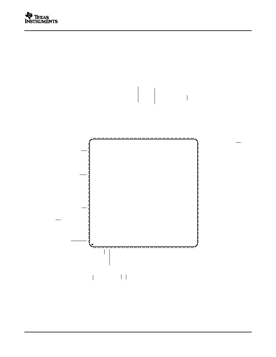
The TMS320F2808, TMS320F2806, TMS320F2802, TMS320F2801/UCD9501, TMS320C2802, and
TMS320C2801 100-pin PZ low-profile quad flatpack (LQFP) pin assignments are shown in
Figure 2-1
,
Figure 2-2
and
Figure 2-3
. The TMS320F2808, TMS320F2806, TMS320F2802, TMS320F2801,
TMS320C2802, and TMS320C2801 100-ball GGM and ZGM ball grid array (BGA) terminal assignments
are shown in
Figure 2-4
.
Table 2-2
describes the function(s) of each pin.
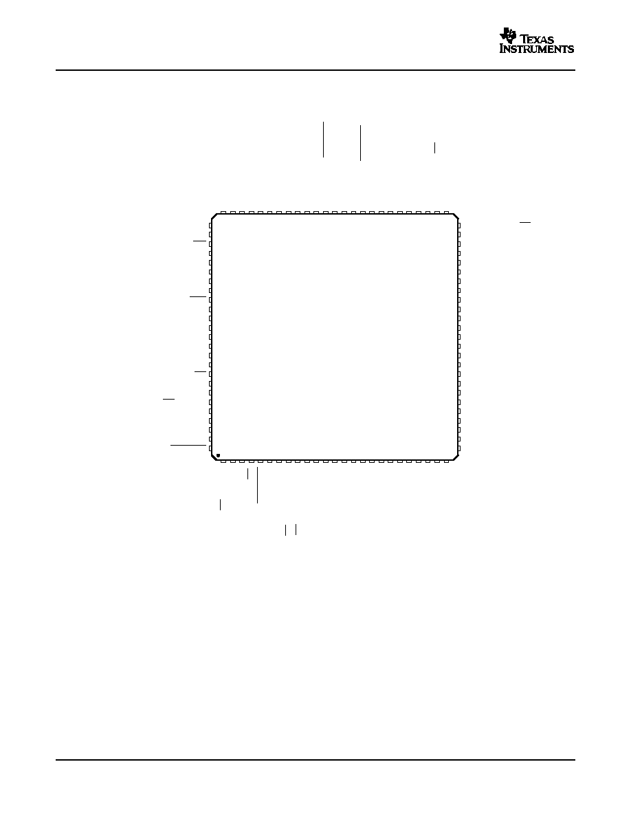
Figure 2-1. TMS320F2808 100-Pin PZ LQFP (Top View)
NOTE: F2809 is pin-compatible to F2808.
Introduction
15
www.ti.com
50
49
48
47
46
45
44
43
42
41
40
39
38
37
36
35
34
33
32
31
30
29
28
27
26
76
77
78
79
80
81
82
83
84
85
86
87
88
89
90
91
92
93
94
95
96
97
98
99
100
75
74
73
72
71
70
69
68
67
66
65
64
63
62
61
60
59
58
57
56
55
54
53
52
51
1
2
3
4
5
6
7
8
9
10
1
1
12
13
14
15
16
17
18
19
20
21
22
23
24
25
GPIO3/EPWM2B/SPISOMID
GPIO0/EPWM1A
GPIO2/EPWM2A
GPIO1/EPWM1B/SPISIMOD
GPIO34
ADCRESEXT
ADCREFP
ADCREFM
ADCREFIN
ADCINB7
ADCINB6
ADCINB5
ADCINB4
ADCINB3
ADCINB2
ADCINB1
ADCINB0
TCK
TMS
TDI
GPIO23/EQEP1I/SPISTEC/SCIRXDB
GPIO22/EQEP1S/SPICLKC/SCITXDB
XCLKOUT
GPIO20/EQEP1A/SPISIMOC
GPIO9/EPWM5B/SCITXDB/ECAP3
GPIO7/EPWM4B/SPISTED/ECAP2
GPIO19/SPISTEA/SCIRXDB
GPIO6/EPWM4A/EPWMSYNCI/EPWMSYNCO
GPIO18/SPICLKA/SCITXDB
GPIO5/EPWM3B/SPICLKD/ECAP1
GPIO4/EPWM3A
GPIO30/CANRXA
GPIO31/CANTXA
ADCINA7
ADCINA6
ADCINA5
ADCINA4
ADCINA3
ADCINA2
ADCINA1
ADCINA0
ADCLO
XRS
TRST
GPIO1
1/EPWM6B/SCIRXDB/ECAP4
GPIO21/EQEP1B/SPISOMIC
V
SS
V
SS
V
DD
V
DDIO
GPIO16/SPISIMOA/TZ5
V
DD2A18
V
SS2AGND
V
DDAIO
V
S
S
V
D
D
V
D
D
I
O
GPIO10/EPWM6A/ADCSOCBO
V
S
S
GPIO8/EPWM5A/ADCSOCAO
V
D
D
V
S
S
GPIO17/SPISOMIA/TZ6
V
DD3VFL
V
SS
V
DD
GPIO28/SCIRXDA/TZ5
V
SS
V
SS
V
DD
V
SS
V
DDIO
GPIO13/TZ2/SPISOMIB
GPIO12/TZ1
/SPISIMOB
GPIO29/SCITXDA/TZ6
GPIO33/SCLA/EPWMSYNCO/ADCSOCBO
GPIO14/TZ3
/SCITXDB/SPICLKB
V
D
D
V
D
D
1
A
1
8
V
S
S
1
A
G
N
D
V
S
S
A
2
V
D
D
A
2
GPIO15/TZ4
/SCIRXDB/SPISTEB
V
S
S
A
I
O
V
S
S
V
D
D
I
O
GPIO32/SDAA/EPWMSYNCI/ADCSOCAO
GPIO26/ECAP3/EQEP2I/SPICLKB
TEST2
TEST1
GPIO25/ECAP2/EQEP2B/SPISOMIB
XCLKIN
X1
X2
GPIO24/ECAP1/EQEP2A/SPISIMOB
EMU1
EMU0
GPIO27/ECAP4/EQEP2S/SPISTEB
TDO
V
S
S
TMS320F2809, TMS320F2808, TMS320F2806
TMS320F2802, TMS320F2801, UCD9501
TMS320C2802, TMS320C2801 Digital Signal Processors
SPRS230G ≠ OCTOBER 2003 ≠ REVISED FEBRUARY 2006
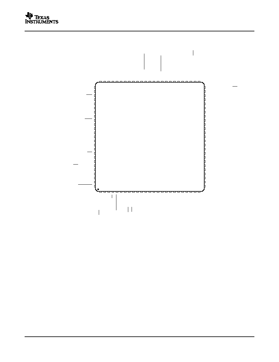
Figure 2-2. TMS320F2806 100-Pin PZ LQFP (Top View)
16
Introduction
www.ti.com
50
49
48
47
46
45
44
43
42
41
40
39
38
37
36
35
34
33
32
31
30
29
28
27
26
76
77
78
79
80
81
82
83
84
85
86
87
88
89
90
91
92
93
94
95
96
97
98
99
100
75
74
73
72
71
70
69
68
67
66
65
64
63
62
61
60
59
58
57
56
55
54
53
52
51
1
2
3
4
5
6
7
8
9
10
1
1
12
13
14
15
16
17
18
19
20
21
22
23
24
25
GPIO0/EPWM1A
GPIO2/EPWM2A
GPIO1/EPWM1B
GPIO34
ADCRESEXT
ADCREFP
ADCREFM
ADCREFIN
ADCINB7
ADCINB6
ADCINB5
ADCINB4
ADCINB3
ADCINB2
ADCINB1
ADCINB0
TCK
TMS
TDI
XCLKOUT
GPIO30/CANRXA
GPIO31/CANTXA
ADCINA7
ADCINA6
ADCINA5
ADCINA4
ADCINA3
ADCINA2
ADCINA1
ADCINA0
ADCLO
XRS
TRST
GPIO12/TZ1
/SPISIMOB
V
S
S
V
D
D
I
O
GPIO29/SCITXDA/TZ6
GPIO33/SCLA/EPWMSYNCO/ADCSOCBO
GPIO14/TZ3
/SPICLKB
V
S
S
V
D
D
V
D
D
1
A
1
8
V
S
S
1
A
G
N
D
V
S
S
A
2
V
D
D
A
2
GPIO32/SDAA/EPWMSYNCI/ADSOCAO
GPIO13/TZ2/SPISOMIB
V
DD3VFL
(A)
V
SS
V
DD
GPIO28/SCIRXDA/TZ5
V
SS
V
SS
V
DD
GPIO21/EQEP1B
V
S
S
V
D
D
GPIO23/EQEP1I
GPIO22/EQEP1S
V
D
D
I
O
GPIO10/ADCSOCBO
GPIO20/EQEP1A
V
S
S
GPIO9
GPIO8/ADCSOCAO
V
D
D
GPIO7/ECAP2
GPIO19/SPISTEA
GPIO6/EPWMSYNCI/EPWMSYNCO
GPIO1
1
V
S
S
GPIO18/SPICLKA
GPIO5/EPWM3B/ECAP1
GPIO17/SPISOMIA/TZ6
GPIO4/EPWM3A
V
SS
V
SS
V
DD
V
DDIO
GPIO16/SPISIMOA/TZ5
GPIO3/EPWM2B
V
DD2A18
V
SS2AGND
V
DDAIO
GPIO15/TZ4
/SPISTEB
V
SS
GPIO27/SPISTEB
V
DDIO
GPIO24/ECAP1/SPISIMOB
V
S
S
A
I
O
GPIO25/ECAP2/SPISIMOB
GPIO26/SPICLKB
TEST2
TEST1
XCLKIN
X1
X2
EMU1
EMU0
TDO
TMS320F2809, TMS320F2808, TMS320F2806
TMS320F2802, TMS320F2801, UCD9501
TMS320C2802, TMS320C2801 Digital Signal Processors
SPRS230G ≠ OCTOBER 2003 ≠ REVISED FEBRUARY 2006
A.
On the C280x devices, the V
DD3VFL
pin is V
DDIO
.
Figure 2-3. TMS320F2802, TMS320F2801/UCD9501, TMS320C2802, TMS320C2801 100-Pin PZ LQFP
(Top View)
Introduction
17
www.ti.com
4
C
B
A
D
E
2
1
3
K
F
G
H
J
5
7
6
9
8
10
Bottom View
TRST
TCK
TDI
TDO
TMS
EMU0
EMU1
V
DD3VFL
TEST1
TEST2
XCLKOUT
XCLKIN
X1
X2
XRS
GPIO0
GPIO1
GPIO2
GPIO3
GPIO4
GPIO5
GPIO6
GPIO7
GPIO9
GPIO8
GPIO10
GPIO11
GPIO12
GPIO13
GPIO14
GPIO15
GPIO16
GPIO17
GPIO18
GPIO19
GPIO20
GPIO21
GPIO22
GPIO23
GPIO24
GPIO25
GPIO26
GPIO27
GPIO28
GPIO29
GPIO30
GPIO31
GPIO32
GPIO33
GPIO34
V
DDA2
V
DD1A18
V
SS1AGND
V
DD
V
DDIO
VSSAIO
V
DDAIO
VSSA2
ADCINA7
V
SS2AGND
V
DD2A18
V
DD
V
DD
V
DD
V
DD
V
DD
V
DDIO
V
DDIO
V
DDIO
VSS
V
SS
V
SS
V
SS
V
SS
VSS
V
SS
V
SS
V
SS
V
SS
V
SS
ADCINB2
ADCINA6
ADCINA5
ADCINA4
ADCINA3
ADCINA2
ADCINA1
ADCINA0
ADCINB7
ADCINB1
ADCINB0
ADCLO
ADCRESEXT
ADCREFIN
ADCREFP
ADCREFM
ADCINB3
ADCINB5
ADCINB4
ADCINB6
TMS320F2809, TMS320F2808, TMS320F2806
TMS320F2802, TMS320F2801, UCD9501
TMS320C2802, TMS320C2801 Digital Signal Processors
SPRS230G ≠ OCTOBER 2003 ≠ REVISED FEBRUARY 2006
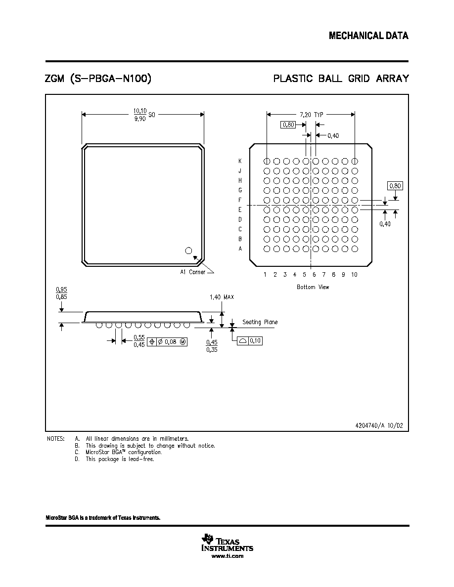
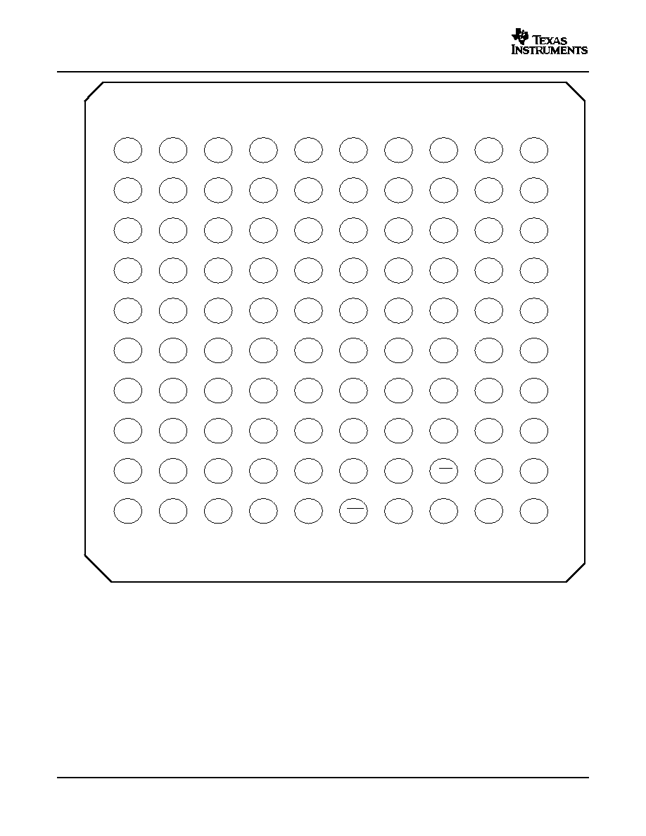
Figure 2-4. TMS320F2808, TMS320F2806,TMS320F2802, TMS320F2801,
TMS320C2802, TMS320C2801 100-Ball GGM and ZGM MicroStar BGATM (Bottom View)
Introduction
18
www.ti.com
2.2
Signal Descriptions
TMS320F2809, TMS320F2808, TMS320F2806
TMS320F2802, TMS320F2801, UCD9501
TMS320C2802, TMS320C2801 Digital Signal Processors
SPRS230G ≠ OCTOBER 2003 ≠ REVISED FEBRUARY 2006
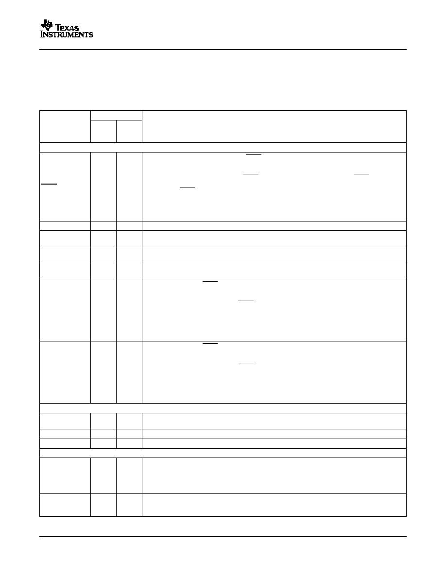
Table 2-2
describes the signals on the 280x devices. All digital inputs are TTL-compatible. All outputs are
3.3 V with CMOS levels. Inputs are not 5-V tolerant.
Table 2-2. Signal Descriptions
PIN NO.
GGM/
NAME
DESCRIPTION
(1)
PZ
ZGM
PIN #
BALL #
JTAG
JTAG test reset with internal pulldown. TRST, when driven high, gives the scan system control of
the operations of the device. If this signal is not connected or driven low, the device operates in its
functional mode, and the test reset signals are ignored.
NOTE: Do not use pullup resistors on TRST; it has an internal pull-down device. TRST is an active
high test pin and must be maintained low at all times during normal device operation. In a low-noise
TRST
84
A6
environment, TRST may be left floating. In other instances, an external pulldown resistor is highly
recommended. The value of this resistor should be based on drive strength of the debugger pods
applicable to the design. A 2.2-k
resistor generally offers adequate protection. Since this is
application-specific, it is recommended that each target board be validated for proper operation of
the debugger and the application. (I,
)
TCK
75
A10
JTAG test clock with internal pullup (I,
)
JTAG test-mode select (TMS) with internal pullup. This serial control input is clocked into the TAP
TMS
74
B10
controller on the rising edge of TCK. (I,
)
JTAG test data input (TDI) with internal pullup. TDI is clocked into the selected register (instruction
TDI
73
C9
or data) on a rising edge of TCK. (I,
)
JTAG scan out, test data output (TDO). The contents of the selected register (instruction or data)
TDO
76
B9
are shifted out of TDO on the falling edge of TCK. (O/Z 8 mA drive)
Emulator pin 0. When TRST is driven high, this pin is used as an interrupt to or from the emulator
system and is defined as input/output through the JTAG scan. This pin is also used to put the
device into boundary-scan mode. With the EMU0 pin at a logic-high state and the EMU1 pin at a
logic-low state, a rising edge on the TRST pin would latch the device into boundary-scan mode.
EMU0
80
A8
(I/O/Z, 8 mA drive
)
NOTE: An external pullup resistor is recommended on this pin. The value of this resistor should be
based on the drive strength of the debugger pods applicable to the design. A 2.2-k
to 4.7-k
resistor is generally adequate. Since this is application-specific, it is recommended that each target
board be validated for proper operation of the debugger and the application.
Emulator pin 1. When TRST is driven high, this pin is used as an interrupt to or from the emulator
system and is defined as input/output through the JTAG scan. This pin is also used to put the
device into boundary-scan mode. With the EMU0 pin at a logic-high state and the EMU1 pin at a
logic-low state, a rising edge on the TRST pin would latch the device into boundary-scan mode.
EMU1
81
B7
(I/O/Z, 8 mA drive
)
NOTE: An external pullup resistor is recommended on this pin. The value of this resistor should be
based on the drive strength of the debugger pods applicable to the design. A 2.2-k
to 4.7-k
resistor is generally adequate. Since this is application-specific, it is recommended that each target
board be validated for proper operation of the debugger and the application.
FLASH
3.3-V Flash Core Power Pin. This pin should be connected to 3.3 V at all times. On the ROM
V
DD3VFL
96
C4
parts (C280x), this pin should be connected to V
DDIO
.
TEST1
97
A3
Test Pin. Reserved for TI. Must be left unconnected. (I/O)
TEST2
98
B3
Test Pin. Reserved for TI. Must be left unconnected. (I/O)
CLOCK
Output clock derived from SYSCLKOUT. XCLKOUT is either the same frequency, one-half the
frequency, or one-fourth the frequency of SYSCLKOUT. This is controlled by the bits 1, 0
XCLKOUT
66
E8
(XCLKOUTDIV) in the XCLK register. At reset, XCLKOUT = SYSCLKOUT/4. The XCLKOUT signal
can be turned off by setting XCLKOUTDIV to 3. Unlike other GPIO pins, the XCLKOUT pin is not
placed in high-impedance state during a reset. (O/Z, 8 mA drive).
External Oscillator Input. This pin is to feed a clock from an external 3.3-V oscillator. In this case,
XCLKIN
90
B5
the X1 pin must be tied to GND. If a crystal/resonator is used (or if an external 1.8-V oscillator is
used to feed clock to X1 pin), this pin must be tied to GND. (I)
(1)
I = Input, O = Output, Z = High impedance, OD = Open drain,
= Pullup,
= Pulldown
Introduction
19
www.ti.com
TMS320F2809, TMS320F2808, TMS320F2806
TMS320F2802, TMS320F2801, UCD9501
TMS320C2802, TMS320C2801 Digital Signal Processors
SPRS230G ≠ OCTOBER 2003 ≠ REVISED FEBRUARY 2006
Table 2-2. Signal Descriptions (continued)
PIN NO.
GGM/
NAME
DESCRIPTION
(1)
PZ
ZGM
PIN #
BALL #
Internal/External Oscillator Input. To use the internal oscillator, a quartz crystal or a ceramic
resonator may be connected across X1 and X2. The X1 pin is referenced to the 1.8-V core digital
X1
88
E6
power supply. A 1.8-V external oscillator may be connected to the X1 pin. In this case, the XCLKIN
pin must be connected to ground. If a 3.3-V external oscillator is used with the XCLKIN pin, X1 must
be tied to GND. (I)
Internal Oscillator Output. A quartz crystal or a ceramic resonator may be connected across X1 and
X2
86
C6
X2. If X2 is not used it must be left unconnected. (O)
RESET
Device Reset (in) and Watchdog Reset (out).
Device reset. XRS causes the device to terminate execution. The PC will point to the address
contained at the location 0x3FFFC0. When XRS is brought to a high level, execution begins at the
location pointed to by the PC. This pin is driven low by the DSP when a watchdog reset occurs.
XRS
78
B8
During watchdog reset, the XRS pin is driven low for the watchdog reset duration of 512 OSCCLK
cycles. (I/OD,
)
The output buffer of this pin is an open-drain with an internal pullup (100
µ
A, typical). It is
recommended that this pin be driven by an open-drain device.
ADC SIGNALS
ADCINA7
16
F3
ADC Group A, Channel 7 input (I)
ADCINA6
17
F4
ADC Group A, Channel 6 input (I)
ADCINA5
18
G4
ADC Group A, Channel 5 input (I)
ADCINA4
19
G1
ADC Group A, Channel 4 input (I)
ADCINA3
20
G2
ADC Group A, Channel 3 input (I)
ADCINA2
21
G3
ADC Group A, Channel 2 input (I)
ADCINA1
22
H1
ADC Group A, Channel 1 input (I)
ADCINA0
23
H2
ADC Group A, Channel 0 input (I)
ADCINB7
34
K5
ADC Group B, Channel 7 input (I)
ADCINB6
33
H4
ADC Group B, Channel 6 input (I)
ADCINB5
32
K4
ADC Group B, Channel 5 input (I)
ADCINB4
31
J4
ADC Group B, Channel 4 input (I)
ADCINB3
30
K3
ADC Group B, Channel 3 input (I)
ADCINB2
29
H3
ADC Group B, Channel 2 input (I)
ADCINB1
28
J3
ADC Group B, Channel 1 input (I)
ADCINB0
27
K2
ADC Group B, Channel 0 input (I)
ADCLO
24
J1
Low Reference (connect to analog ground) (I)
ADCRESEXT
38
F5
ADC External Current Bias Resistor. Connect a 22-k
resistor to analog ground.
ADCREFIN
35
J5
External reference input (I)
Internal Reference Positive Output. Requires a low ESR (50 m
- 1.5
) ceramic bypass capacitor
ADCREFP
37
G5
of 2.2
µ
F to analog ground. (O)
Internal Reference Medium Output. Requires a low ESR (50 m
- 1.5
) ceramic bypass capacitor
ADCREFM
36
H5
of 2.2
µ
F to analog ground. (O)
CPU AND I/O POWER PINS
V
DDA2
15
F2
ADC Analog Power Pin (3.3 V)
V
SSA2
14
F1
ADC Analog Ground Pin
V
DDAIO
26
J2
ADC Analog I/O Power Pin (3.3 V)
V
SSAIO
25
K1
ADC Analog I/O Ground Pin
V
DD1A18
12
E4
ADC Analog Power Pin (1.8 V)
V
SS1AGND
13
E5
ADC Analog Ground Pin
V
DD2A18
40
J6
ADC Analog Power Pin (1.8 V)
V
SS2AGND
39
K6
ADC Analog Ground Pin
20
Introduction
www.ti.com
TMS320F2809, TMS320F2808, TMS320F2806
TMS320F2802, TMS320F2801, UCD9501
TMS320C2802, TMS320C2801 Digital Signal Processors
SPRS230G ≠ OCTOBER 2003 ≠ REVISED FEBRUARY 2006
Table 2-2. Signal Descriptions (continued)
PIN NO.
GGM/
NAME
DESCRIPTION
(1)
PZ
ZGM
PIN #
BALL #
V
DD
10
E2
V
DD
42
G6
V
DD
59
F10
CPU and Logic Digital Power Pins (1.8 V)
V
DD
68
D7
V
DD
85
B6
V
DD
93
D4
V
DDIO
3
C2
V
DDIO
46
H7
Digital I/O Power Pin (3.3 V)
V
DDIO
65
E9
V
DDIO
82
A7
V
SS
2
B1
V
SS
11
E3
V
SS
41
H6
V
SS
49
K9
V
SS
55
H10
V
SS
62
F7
Digital Ground Pins
V
SS
69
D10
V
SS
77
A9
V
SS
87
D6
V
SS
89
A5
V
SS
94
A4
GPIOA AND PERIPHERAL SIGNALS
(2)
GPIO0
General purpose input/output 0 (I/O/Z)
(3)
EPWM1A
Enhanced PWM1 Output A and HRPWM channel (O)
47
K8
-
-
-
-
GPIO1
General purpose input/output 1 (I/O/Z)
(3)
EPWM1B
Enhanced PWM1 Output B (O)
44
K7
SPISIMOD
SPI-D slave in, master out (I/O) (not available on 2801/9501, 2802)
-
-
GPIO2
General purpose input/output 2 (I/O/Z)
(3)
EPWM2A
Enhanced PWM2 Output A and HRPWM channel (O)
45
J7
-
-
-
-
GPIO3
General purpose input/output 3 (I/O/Z)
(3)
EPWM2B
Enhanced PWM2 Output B (O)
48
J8
SPISOMID
SPI-D slave out, master in (I/O) (not available on 2801/9501, 2802)
-
-
GPIO4
General purpose input/output 4 (I/O/Z)
(3)
EPWM3A
Enhanced PWM3 output A and HRPWM channel (O)
51
J9
-
-
-
-
GPIO5
General purpose input/output 5 (I/O/Z)
(3)
EPWM3B
Enhanced PWM3 output B (O)
53
H9
SPICLKD
SPI-D clock (I/O) (not available on 2801/9501, 2802)
ECAP1
Enhanced capture input/output 1 (I/O)
(2)
All GPIO pins are I/O/Z, 4-mA drive typical (unless otherwise indicated), and have an internal pullup, which can be selectively
enabled/disabled on a per-pin basis. This feature only applies to the GPIO pins. The GPIO function (shown in Italics) is the default at
reset. The peripheral signals that are listed under them are alternate functions.
(3)
The pullups on GPIO0-GPIO11 pins are not enabled at reset.
Introduction
21
www.ti.com
TMS320F2809, TMS320F2808, TMS320F2806
TMS320F2802, TMS320F2801, UCD9501
TMS320C2802, TMS320C2801 Digital Signal Processors
SPRS230G ≠ OCTOBER 2003 ≠ REVISED FEBRUARY 2006
Table 2-2. Signal Descriptions (continued)
PIN NO.
GGM/
NAME
DESCRIPTION
(1)
PZ
ZGM
PIN #
BALL #
GPIO6
General purpose input/output 6 (I/O/Z)
(3)
EPWM4A
Enhanced PWM4 output A and HRPWM channel (not available on 2801/9501, 2802) (O)
56
G9
EPWMSYNCI
External ePWM sync pulse input (I)
EPWMSYNCO
External ePWM sync pulse output (O)
GPIO7
General purpose input/output 7 (I/O/Z)
(3)
EPWM4B
Enhanced PWM4 output B (not available on 2801/9501, 2802) (O)
58
G8
SPISTED
SPI-D slave transmit enable (not available on 2801/9501, 2802) (I/O)
ECAP2
Enhanced capture input/output 2 (I/O)
GPIO8
General purpose input/output 8 (I/O/Z)
(3)
EPWM5A
Enhanced PWM5 output A (not available on 2801/9501, 2802) (O)
60
F9
CANTXB
Enhanced CAN-B transmit (not available on 2801/9501, 2802, F2806) (O)
ADCSOCAO
ADC start-of-conversion A (O)
GPIO9
General purpose input/output 9 (I/O/Z)
(3)
EPWM5B
Enhanced PWM5 output B (not available on 2801/9501, 2802) (O)
61
F8
SCITXDB
SCI-B transmit data (not available on 2801/9501, 2802) (O)
ECAP3
Enhanced capture input/output 3 (not available on 2801/9501, 2802) (I/O)
GPIO10
General purpose input/output 10 (I/O/Z)
(3)
EPWM6A
Enhanced PWM6 output A (not available on 2801/9501, 2802) (O)
64
E10
CANRXB
Enhanced CAN-B receive (not available on 2801/9501, 2802, F2806) (I)
ADCSOCBO
ADC start-of-conversion B (O)
GPIO11
General purpose input/output 11 (I/O/Z)
(3)
EPWM6B
Enhanced PWM6 output B (not available on 2801/9501, 2802) (O)
70
D9
SCIRXDB
SCI-B receive data (not available on 2801/9501, 2802) (I)
ECAP4
Enhanced CAP Input/Output 4 (not available on 2801/9501, 2802) (I/O)
GPIO12
General purpose input/output 12 (I/O/Z)
(4)
TZ1
Trip Zone input 1 (I)
1
B2
CANTXB
Enhanced CAN-B transmit (not available on 2801/9501, 2802, F2806) (O)
SPISIMOB
SPI-B Slave in, Master out (I/O)
GPIO13
General purpose input/output 13 (I/O/Z)
(4)
TZ2
Trip zone input 2 (I)
95
B4
CANRXB
Enhanced CAN-B receive (not available on 2801/9501, 2802, F2806) (I)
SPISOMIB
SPI-B slave out, master in (I/O)
GPIO14
General purpose input/output 14 (I/O/Z)
(4)
TZ3
Trip zone input 3 (I)
8
D3
SCITXDB
SCI-B transmit (not available on 2801/9501, 2802) (O)
SPICLKB
SPI-B clock input/output (I/O)
GPIO15
General purpose input/output 15 (I/O/Z)
(4)
TZ4
Trip zone input (I)
9
E1
SCIRXDB
SCI-B receive (not available on 2801/9501, 2802) (I)
SPISTEB
SPI-B slave transmit enable (I/O)
GPIO16
General purpose input/output 16 (I/O/Z)
(4)
SPISIMOA
SPI-A slave in, master out (I/O)
50
K10
CANTXB
Enhanced CAN-B transmit (not available on 2801/9501, 2802, F2806) (O)
TZ5
Trip zone input 5 (I)
GPIO17
General purpose input/output 17 (I/O/Z)
(4)
SPISOMIA
SPI-A slave out, master in (I/O)
52
J10
CANRXB
Enhanced CAN-B receive (not available on 2801/9501, 2802, F2806) (I)
TZ6
Trip zone input 6(I)
GPIO18
General purpose input/output 18 (I/O/Z)
(4)
SPICLKA
SPI-A clock input/output (I/O)
SCITXDB
54
H8
SCI-B transmit (not available on 2801/9501, 2802) (O)
-
-
-
-
GPIO19
General purpose input/output 19 (I/O/Z)
(4)
SPISTEA
SPI-A slave transmit enable input/output (I/O)
SCIRXDB
57
G10
SCI-B receive (not available on 2801/9501, 2802) (I)
-
-
-
-
(4)
The pullups on GPIO12-GPIO34 are enabled upon reset.
22
Introduction

www.ti.com
TMS320F2809, TMS320F2808, TMS320F2806
TMS320F2802, TMS320F2801, UCD9501
TMS320C2802, TMS320C2801 Digital Signal Processors
SPRS230G ≠ OCTOBER 2003 ≠ REVISED FEBRUARY 2006
Table 2-2. Signal Descriptions (continued)
PIN NO.
GGM/
NAME
DESCRIPTION
(1)
PZ
ZGM
PIN #
BALL #
GPIO20
General purpose input/output 20 (I/O/Z)
(4)
EQEP1A
Enhanced QEP1 input A (I)
63
F6
SPISIMOC
SPI-C slave in, master out (not available on 2801/9501, 2802) (I/O)
CANTXB
Enhanced CAN-B transmit (not available on 2801/9501, 2802, F2806) (O)
GPIO21
General purpose input/output 21 (I/O/Z)
(4)
EQEP1B
Enhanced QEP1 input A (I)
67
E7
SPISOMIC
SPI-C master in, slave out (not available on 2801/9501, 2802) (I/O)
CANRXB
Enhanced CAN-B receive (not available on 2801/9501, 2802, F2806) (I)
GPIO22
General purpose input/output 22 (I/O/Z)
(4)
EQEP1S
Enhanced QEP1 strobe (I/O)
71
D8
SPICLKC
SPI-C clock (not available on 2801/9501, 2802) (I/O)
SCITXDB
SCI-B transmit (not available on 2801/9501, 2802) (O)
GPIO23
General purpose input/output 23 (I/O/Z)
(4)
EQEP1I
Enhanced QEP1 index (I/O)
72
C10
SPISTEC
SPI-C slave transmit enable (not available on 2801/9501, 2802) (I/O)
SCIRXDB
SCI-B receive (I) (not available on 2801/9501, 2802)
GPIO24
General purpose input/output 24 (I/O/Z)
(4)
ECAP1
Enhanced capture 1 (I/O)
83
C7
EQEP2A
Enhanced QEP2 input A (I) (not available on 2801/9501, 2802)
SPISIMOB
SPI-B slave in, master out (I/O)
GPIO25
General purpose input/output 25 (I/O/Z)
(4)
ECAP2
Enhanced capture 2 (I/O)
91
C5
EQEP2B
Enhanced QEP2 input B (I) (not available on 2801/9501, 2802)
SPISOMIB
SPI-B master in, slave out (I/O)
GPIO26
General purpose input/output 26 (I/O/Z)
(4)
ECAP3
Enhanced capture 3 (I/O) (not available on 2801/9501, 2802)
99
A2
EQEP2I
Enhanced QEP2 index (I/O) (not available on 2801/9501, 2802)
SPICLKB
SPI-B clock (I/O)
GPIO27
General purpose input/output 27 (I/O/Z)
(4)
ECAP4
Enhanced capture 4 (I/O) (not available on 2801/9501, 2802)
79
C8
EQEP2S
Enhanced QEP2 strobe (I/O) (not available on 2801, 2802)
SPISTEB
SPI-B slave transmit enable (I/O)
GPIO28
General purpose input/output 28. This pin has an 8-mA (typical) output buffer. (I/O/Z)
(4)
SCIRXDA
SCI receive data (I)
92
D5
-
-
TZ5
Trip zone 5 (I)
GPIO29
General purpose input/output 29. This pin has an 8-mA (typical) output buffer. (I/O/Z)
(4)
SCITXDA
SCI transmit data (O)
4
C3
-
-
TZ6
Trip zone 6 (I)
GPIO30
General purpose input/output 30. This pin has an 8-mA (typical) output buffer. (I/O/Z)
(4)
CANRXA
Enhanced CAN-A receive data (I)
6
D2
-
-
-
-
GPIO31
General purpose input/output 31. This pin has an 8-mA (typical) output buffer. (I/O/Z)
(4)
CANTXA
Enhanced CAN-A transmit data (O)
7
D1
-
-
-
-
GPIO32
General purpose input/output 32 (I/O/Z)
(4)
SDAA
I2C data open-drain bidirectional port (I/OD)
100
A1
EPWMSYNCI
Enhanced PWM external sync pulse input (I)
ADCSOCAO
ADC start-of-conversion (O)
Introduction
23
www.ti.com
TMS320F2809, TMS320F2808, TMS320F2806
TMS320F2802, TMS320F2801, UCD9501
TMS320C2802, TMS320C2801 Digital Signal Processors
SPRS230G ≠ OCTOBER 2003 ≠ REVISED FEBRUARY 2006
Table 2-2. Signal Descriptions (continued)
PIN NO.
GGM/
NAME
DESCRIPTION
(1)
PZ
ZGM
PIN #
BALL #
GPIO33
General-Purpose Input/Output 33 (I/O/Z)
(1)
SCLA
I2C clock open-drain bidirectional port (I/OD)
5
C1
EPWMSYNCO
Enhanced PWM external synch pulse output (O)
ADCSOCBO
ADC start-of-conversion (O)
GPIO34
General-Purpose Input/Output 34 (I/O/Z)
(1)
-
-
43
G7
-
-
-
-
(1)
The pullups on GPIO12-GPIO34 are enabled upon reset.
24
Introduction
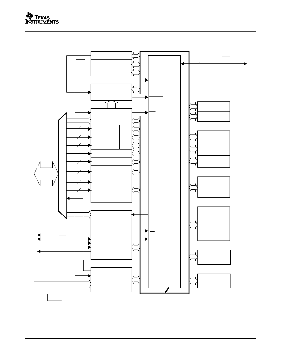
www.ti.com
3
Functional Overview
° ° ° ° °
° ° ° ° °
° ° ° ° °
° ° ° ° °
° ° ° ° °
° ° ° ° °
° ° ° ° °
° ° ° ° °
° ° ° ° °
° ° ° ° °
° ° ° ° °
INT[12:1]
Real-Time JTAG
(TDI, TDO, TRST, TCK,
TMS, EMU0, EMU1)
C28x CPU
(100 MHz)
NMI, INT13
Memory Bus
Boot ROM
4 K
y
16
(1-wait state)
FLASH
128K
x 16 (F2809)
64K
x 16 (F2808)
32K x 16 (F2806)
32K
x 16 (F2802)
16K x 16 (F2801)
16K x 16 (9501)
H0 SARAM
(C)
8 K
y
16
(0-wait)
L1 SARAM
(B)
4 K
y
16
(0-wait)
L0 SARAM
4 K
y
16
(0-wait)
M0 SARAM
1 K
y
16
M1 SARAM
1 K
y
16
INT14
32-bit CPU TIMER 0
32-bit CPU TIMER 1
32-bit CPU TIMER 2
SYSCLKOUT
RS
CLKIN
12-Bit ADC
ADCSOCA/B
SOCA/B
16 Channels
12
6
32
XCLKOUT
XRS
XCLKIN
X1
X2
32
System Control
(Oscillator, PLL,
Peripheral Clocking,
Low Power Modes,
WatchDog)
ePWM1/2/3/4/5/6
(12 PWM outputs,
6 trip zones,
6 timers 16-bit)
eCAP1/2/3/4
(4 timers 32-bit)
eQEP1/2
eCAN-A/B (32 mbox)
External Interrupt
Control
PIE
(96 Interrupts)
(A)
FIFO
FIFO
FIFO
SCI-A/B
SPI-A/B/C/D
I
2
C-A
4
8
4
2
16
4
GPIO MUX
GPIOs
(35)
TINT0
TINT1
TINT2
7
° ° ° ° °
° ° ° ° °
° ° ° ° °
OTP
(D)
1K
y
16
Peripheral Bus
¢°¢°¢
¢°¢°¢
Protected by the code-security module.
° ° ° ° °
° ° ° ° °
° ° ° ° °
° ° ° ° °
ROM
32K
x 16 (C2802)
16K x 16 (C2801)
TMS320F2809, TMS320F2808, TMS320F2806
TMS320F2802, TMS320F2801, UCD9501
TMS320C2802, TMS320C2801 Digital Signal Processors
SPRS230G ≠ OCTOBER 2003 ≠ REVISED FEBRUARY 2006
A.
43 of the possible 96 interrupts are used on the devices.
B.
Not available in F2802, F2801/9501, C2802, and C2801.
C.
Not available in F2806, F2802, F2801/9501, C2802, and C2801.
D.
The 1K x 16 OTP has been replaced with 1K x 16 ROM for C280x devices.
Figure 3-1. Functional Block Diagram
Functional Overview
25
www.ti.com
3.1
Memory Map
° ¢ ¢ ¢ ¢ ¢ ¢ ¢ ¢ ¢
° ¢ ¢ ¢ ¢ ¢ ¢ ¢ ¢ ¢
° ¢ ¢ ¢ ¢
° ¢ ¢ ¢ ¢
° ¢ ¢ ¢ ¢
0x00 0000
Block Start
Address
Data Space
Prog Space
M0 SARAM (1 K
y
16)
M1 SARAM (1 K
y
16)
0x00 0400
Peripheral Frame 0
0x00 0800
° ¢ ¢ ¢ ¢
° ¢ ¢ ¢ ¢
0x00 0D00
Peripheral Frame 1
(protected)
0x00 6000
Peripheral Frame 2
(protected)
0x00 7000
L0 SARAM (0-wait)
(4 k
y
16, Secure Zone, Dual Mapped)
0x00 8000
L1 SARAM (0-wait)
(4 k
y
16, Secure Zone, Dual Mapped)
0x00 9000
H0 SARAM (0-wait)
(8 k
y
16, Dual Mapped)
0x00 A000
0x00 C000
OTP
(1 k
y
16, Secure Zone)
0x3D 7800
0x3D 7C00
FLASH
(64 k
y
16, Secure Zone)
0x3E 8000
0x3F 7FF8
128-bit Password
L0 SARAM (0-wait)
(4 k
y
16, Secure Zone, Dual Mapped)
0x3F 8000
L1 SARAM (0-wait)
(4 k
y
16, Secure Zone, Dual Mapped)
0x3F 9000
H0 SARAM (0-wait)
(8 k
y
16, Dual Mapped)
0x3F A000
0x3F F000
° ¢ ¢ ¢ ¢ ¢ ¢ ¢ ¢ ¢
° ¢ ¢ ¢ ¢ ¢ ¢ ¢ ¢ ¢
Boot ROM (4 k
y
16)
Vectors (32
y
32)
(enabled if VMAP = 1, ENPIE = 0)
0x3F FFC0
Low 64K [0000 - FFFF]
(24x/240x equivalent data space)
High 64K [3F0000 - 3FFFFF]
(24x/240x equivalent program space)
° ¢
° ¢
Reserved
° ¢ ¢ ¢ ¢ ¢ ¢ ¢ ¢ ¢
° ¢ ¢ ¢ ¢ ¢ ¢ ¢ ¢ ¢
° ¢ ¢ ¢ ¢ ¢ ¢ ¢ ¢ ¢
° ¢ ¢ ¢ ¢ ¢ ¢ ¢ ¢ ¢
° ¢ ¢ ¢ ¢ ¢ ¢ ¢ ¢ ¢
° ¢ ¢ ¢ ¢ ¢ ¢ ¢ ¢ ¢
° ¢ ¢ ¢ ¢
° ¢ ¢ ¢ ¢
° ¢ ¢ ¢ ¢
° ¢ ¢ ¢ ¢
° ¢ ¢ ¢ ¢
PIE Vector - RAM
(256 x 16)
(Enabled if ENPIE = 1)
0x00 0E00
0x3F C000
TMS320F2809, TMS320F2808, TMS320F2806
TMS320F2802, TMS320F2801, UCD9501
TMS320C2802, TMS320C2801 Digital Signal Processors
SPRS230G ≠ OCTOBER 2003 ≠ REVISED FEBRUARY 2006
A.
Memory blocks are not to scale.
B.
Peripheral Frame 0, Peripheral Frame 1, and Peripheral Frame 2 memory maps are restricted to data memory only.
User program cannot access these memory maps in program space.
C.
" Protected" means the order of Write followed by Read operations is preserved rather than the pipeline order.
D.
Certain memory ranges are EALLOW protected against spurious writes after configuration.
Figure 3-2. F2808 Memory Map
26
Functional Overview
www.ti.com
° ° ° ° ° ° ° ° °
° ° ° ° ° ° ° ° °
° ° ° ° ° ° ° ° °
0x00 0000
Block Start
Address
Data Space
M0 SARAM (1K
y
16)
0x00 0400
0x00 0800
0x00 0D00
0x00 6000
0x00 7000
0x00 8000
0x00 9000
0x00 A000
0x3D 7800
0x3D 7C00
0x3F 7FF8
0x3F 8000
0x3F 9000
0x3F A000
0x3F F000
0x3F FFC0
OTP
(1 K
y
16, Secure Zone)
FLASH
(32 K
y
16, Secure Zone)
° ° ° ° ° ° ° ° °
° ° ° ° ° ° ° ° °
° ° ° ° ° ° ° ° °
Boot ROM (4 K
y
16)
Low 64K [0000-FFFF]
(24x/240x equivalent data space)
High 64K [3F0000 -3FFFF]
(24x/240x equivalent program space)
° ° °
° ° °
Reserved
M1 SARAM (1K
y
16)
L0 SARAM (0-wait)
(4k
y
16, Secure Zone, Dual Mapped)
L1 SARAM (0-wait)
(4k
y
16, Secure Zone, Dual Mapped)
L0 SARAM (0-wait) (4k
y
16,
Secure Zone, Dual Mapped)
L1 SARAM (0-wait) (4k
y
16,
Secure Zone, Dual Mapped)
128-bit Password
0x3F 0000
Prog Space
° ° ° ° ° ° ° ° °
° ° ° ° ° ° ° ° °
° ° ° ° ° ° ° ° °
° ° ° ° ° ° ° ° °
° ° ° ° ° ° ° ° °
° ° ° ° ° ° ° ° °
° ° ° ° ° ° ° ° °
° ° ° °
° ° ° °
° ° ° °
° ° ° °
Peripheral Frame 0
° ° ° ° °
° ° ° ° °
Peripheral Frame 1
(protected)
Peripheral Frame 2
(protected)
° ° ° °
° ° ° °
° ° ° °
° ° ° °
° ° ° °
PIE Vector - RAM
(256 x 16)
(Enabled if ENPIE = 1)
Vectors (32
y
32)
(enabled if VMAP = 1, ENPIE = 0)
0x00 0E00
TMS320F2809, TMS320F2808, TMS320F2806
TMS320F2802, TMS320F2801, UCD9501
TMS320C2802, TMS320C2801 Digital Signal Processors
SPRS230G ≠ OCTOBER 2003 ≠ REVISED FEBRUARY 2006
A.
Memory blocks are not to scale.
B.
Peripheral Frame 0, Peripheral Frame 1, and Peripheral Frame 2 memory maps are restricted to data memory only.
User program cannot access these memory maps in program space.
C.
" Protected" means the order of Write followed by Read operations is preserved rather than the pipeline order.
D.
Certain memory ranges are EALLOW protected against spurious writes after configuration.
Figure 3-3. F2806 Memory Map
Functional Overview
27

www.ti.com
0x00 0000
Block Start
Address
0x00 0400
0x00 0800
0x00 0D00
0x00 6000
0x00 7000
0x00 8000
0x00 9000
0x3D 7800
0x3F 0000
0x3F 7FF8
0x3F 8000
0x3F 9000
0x3F F000
0x3F FFC0
° ° ° ° ° ° ° ° °
° ° ° ° ° ° ° ° °
° ° ° ° ° ° ° ° °
° ° ° ° ° ° ° ° °
° ° ° ° ° ° ° ° °
° ° ° ° ° ° ° ° °
° ° ° ° ° ° ° ° °
° ° ° ° ° ° ° ° °
OTP (F2802 Only)
(A)
(1K
y
16, Secure Zone)
° ° ° ° ° ° ° ° °
° ° ° ° ° ° ° ° °
° ° ° ° ° ° ° ° °
FLASH (F2802) or ROM (C2802)
(32K
y
16, Secure Zone)
L0 (0-wait)
(4K
y
16, Secure Zone, Dual Mapped)
° ° ° ° ° ° ° ° °
° ° ° ° ° ° ° ° °
° ° ° ° ° ° ° ° °
° ° ° ° ° ° ° ° °
Boot ROM (4 K
y
16)
° °
° °
Reserved
128-bit Password
Data Space
Prog Space
0x3D 7C00
Vectors (32
y
32)
(enabled if VMAP = 1, ENPIE = 0)
Low 64K [0000-FFFF]
(24x/240x equivalent data space)
High 64K [3F0000 -3FFFF]
(24x/240x equivalent program space)
° ° ° ° °
° ° ° ° °
° ° ° ° °
° ° ° ° °
M0 SARAM (1K
y
16)
M1 SARAM (1K
y
16)
Peripheral Frame 0
° ° ° °
° ° ° °
Peripheral Frame 1
(protected)
Peripheral Frame 2
(protected)
L0 SARAM (0-wait)
(4K
y
16, Secure Zone, Dual Mapped)
° ° ° ° °
° ° ° ° °
° ° ° ° °
° ° ° ° °
° ° ° ° °
PIE Vector - RAM
(256 x 16)
(Enabled if ENPIE = 1)
0x00 0E00
TMS320F2809, TMS320F2808, TMS320F2806
TMS320F2802, TMS320F2801, UCD9501
TMS320C2802, TMS320C2801 Digital Signal Processors
SPRS230G ≠ OCTOBER 2003 ≠ REVISED FEBRUARY 2006
A.
The 1K x 16 OTP has been replaced with 1K x 16 ROM in C2802.
B.
Memory blocks are not to scale.
C.
Peripheral Frame 0, Peripheral Frame 1, and Peripheral Frame 2 memory maps are restricted to data memory only.
User program cannot access these memory maps in program space.
D.
" Protected" means the order of Write followed by Read operations is preserved rather than the pipeline order.
E.
Certain memory ranges are EALLOW protected against spurious writes after configuration.
Figure 3-4. F2802, C2802 Memory Map
28
Functional Overview
www.ti.com
0x00 0000
Block Start
Address
0x00 0400
0x00 0800
0x00 0D00
0x00 6000
0x00 7000
0x00 8000
0x00 9000
0x3D 7800
0x3F 4000
0x3F 7FF8
0x3F 8000
0x3F 9000
0x3F F000
0x3F FFC0
° ° ° ° ° ° ° ° °
° ° ° ° ° ° ° ° °
° ° ° ° ° ° ° ° °
° ° ° ° ° ° ° ° °
° ° ° ° ° ° ° ° °
° ° ° ° ° ° ° ° °
° ° ° ° ° ° ° ° °
° ° ° ° ° ° ° ° °
OTP (F2801/9501 Only)
(A)
(1K
y
16, Secure Zone)
° ° ° ° ° ° ° ° °
° ° ° ° ° ° ° ° °
° ° ° ° ° ° ° ° °
FLASH (F2801/9501) or ROM (C2801)
(16K
y
16, Secure Zone)
L0 (0-wait)
(4K
y
16, Secure Zone, Dual Mapped)
° ° ° ° ° ° ° ° °
° ° ° ° ° ° ° ° °
° ° ° ° ° ° ° ° °
° ° ° ° ° ° ° ° °
Boot ROM (4K
y
16)
° °
° °
Reserved
128-bit Password
Data Space
Prog Space
0x3D 7C00
Vectors (32
y
32)
(enabled if VMAP = 1, ENPIE = 0)
Low 64K [0000-FFFF]
(24x/240x equivalent data space)
High 64K [3F0000 -3FFFF]
(24x/240x equivalent program space)
° ° ° ° °
° ° ° ° °
° ° ° ° °
° ° ° ° °
M0 SARAM (1K
y
16)
M1 SARAM (1K
y
16)
Peripheral Frame 0
° ° ° °
° ° ° °
Peripheral Frame 1
(protected)
Peripheral Frame 2
(protected)
L0 SARAM (0-wait)
(4K
y
16, Secure Zone, Dual Mapped)
° ° ° ° °
° ° ° ° °
° ° ° ° °
° ° ° ° °
° ° ° ° °
PIE Vector - RAM
(256 x 16)
(Enabled if ENPIE = 1)
0x00 0E00
TMS320F2809, TMS320F2808, TMS320F2806
TMS320F2802, TMS320F2801, UCD9501
TMS320C2802, TMS320C2801 Digital Signal Processors
SPRS230G ≠ OCTOBER 2003 ≠ REVISED FEBRUARY 2006
A.
The 1K x 16 OTP has been replaced with 1K x 16 ROM in C2801.
B.
Memory blocks are not to scale.
C.
Peripheral Frame 0, Peripheral Frame 1, and Peripheral Frame 2 memory maps are restricted to data memory only.
User program cannot access these memory maps in program space.
D.
" Protected" means the order of Write followed by Read operations is preserved rather than the pipeline order.
E.
Certain memory ranges are EALLOW protected against spurious writes after configuration.
Figure 3-5. F2801/9501, C2801 Memory Map
Functional Overview
29

www.ti.com
TMS320F2809, TMS320F2808, TMS320F2806
TMS320F2802, TMS320F2801, UCD9501
TMS320C2802, TMS320C2801 Digital Signal Processors
SPRS230G ≠ OCTOBER 2003 ≠ REVISED FEBRUARY 2006
Table 3-1. Addresses of Flash Sectors in F2809
ADDRESS RANGE
PROGRAM AND DATA SPACE
0x3D 8000
Sector H (16K x 16)
0x3D BFFF
0x3D C000
Sector G (16K x 16)
0x3D FFFF
0x3E 0000
Sector F (16K x 16)
0x3E 3FFF
0x3E 4000
Sector E (16K x 16)
0x3E 7FFF
0x3E 8000
Sector D (16K x 16)
0x3E BFFF
0x3E C000
Sector C (16K x 16)
0x3E FFFF
0x3F 0000
Sector B (16K x 16)
0x3F 3FFF
0x3F 4000
Sector A (16K x 16)
0x3F 7F7F
0x3F 7F80
Program to 0x0000 when using the
0x3F 7FF5
Code Security Module
0x3F 7FF6
Boot-to-Flash Entry Point
0x3F 7FF7
(program branch instruction here)
0x3F 7FF8
Security Password (128-Bit)
0x3F 7FFF
(Do not program to all zeros)
Table 3-2. Addresses of Flash Sectors in F2808
ADDRESS RANGE
PROGRAM AND DATA SPACE
0x3E 8000
Sector D (16K x 16)
0x3E BFFF
0x3E C000
Sector C (16K x 16)
0x3E FFFF
0x3F 0000
Sector B (16K x 16)
0x3F 3FFF
0x3F 4000
Sector A (16K x 16)
0x3F 7F7F
0x3F 7F80
Program to 0x0000 when using the
0x3F 7FF5
Code Security Module
0x3F 7FF6
Boot-to-Flash Entry Point
0x3F 7FF7
(program branch instruction here)
0x3F 7FF8
Security Password (128-Bit)
0x3F 7FFF
(Do not program to all zeros)
Functional Overview
30

www.ti.com
TMS320F2809, TMS320F2808, TMS320F2806
TMS320F2802, TMS320F2801, UCD9501
TMS320C2802, TMS320C2801 Digital Signal Processors
SPRS230G ≠ OCTOBER 2003 ≠ REVISED FEBRUARY 2006
Table 3-3. Addresses of Flash Sectors in F2806, F2802
ADDRESS RANGE
PROGRAM AND DATA SPACE
0x3F 0000
Sector D (8K x 16)
0x3F 1FFF
0x3F 2000
Sector C (8K x 16)
0x3F 3FFF
0x3F 4000
Sector B (8K x 16)
0x3F 5FFF
0x3F 6000
Sector A (8K x 16)
0x3F 7F7F
0x3F 7F80
Program to 0x0000 when using the
0x3F 7FF5
Code Security Module
0x3F 7FF6
Boot-to-Flash Entry Point
0x3F 7FF7
(program branch instruction here)
0x3F 7FF8
Security Password (128-Bit)
0x3F 7FFF
(Do not program to all zeros)
Table 3-4. Addresses of Flash Sectors in F2801/9501
ADDRESS RANGE
PROGRAM AND DATA SPACE
0x3F 4000
Sector D (4K x 16)
0x3F 4FFF
0x3F 5000
Sector C (4K x 16)
0x3F 5FFF
0x3F 6000
Sector B (4K x 16)
0x3F 6FFF
0x3F 7000
Sector A (4K x 16)
0x3F 7F7F
0x3F 7F80
Program to 0x0000 when using the
0x3F 7FF5
Code Security Module
0x3F 7FF6
Boot-to-Flash Entry Point
0x3F 7FF7
(program branch instruction here)
0x3F 7FF8
Security Password (128-Bit)
0x3F 7FFF
(Do not program to all zeros)
NOTE
For code security operation, all addresses between 0x3F7F80 and 0x3F7FF5 cannot be
used as program code or data, but must be programmed to 0x0000 when the
code-security passwords are programmed. If security is not a concern, addresses
0x3F7F80 through 0x3F7FEF may be used for code or data. Addresses 0x3F7FF0 ≠
0x3F7FF5 are reserved for data variables and should not contain program code.
Peripheral Frame 1 and Peripheral Frame 2 are grouped together so as to enable these blocks to be
write/read peripheral block protected. The protected mode ensures that all accesses to these blocks
happen as written. Because of the C28x pipeline, a write immediately followed by a read, to different
memory locations, will appear in reverse order on the memory bus of the CPU. This can cause problems
in certain peripheral applications where the user expected the write to occur first (as written). The C28x
CPU supports a block protection mode where a region of memory can be protected so as to make sure
that operations occur as written (the penalty is extra cycles are added to align the operations). This mode
is programmable and by default, it will protect the selected zones.
The wait states for the various spaces in the memory map area are listed in
Table 3-5
.
Functional Overview
31

www.ti.com
3.2
Brief Descriptions
3.2.1
C28x CPU
3.2.2
Memory Bus (Harvard Bus Architecture)
TMS320F2809, TMS320F2808, TMS320F2806
TMS320F2802, TMS320F2801, UCD9501
TMS320C2802, TMS320C2801 Digital Signal Processors
SPRS230G ≠ OCTOBER 2003 ≠ REVISED FEBRUARY 2006
Table 3-5. Wait States
AREA
WAIT-STATES
COMMENTS
M0 and M1 SARAMs
0-wait
Fixed
Peripheral Frame 0
0-wait
Fixed
0-wait (writes)
Peripheral Frame 1
Fixed. The eCAN peripheral can extend a cycle as needed.
2-wait (reads)
0-wait (writes)
Peripheral Frame 2
Fixed
2-wait (reads)
L0 & L1 SARAMs
0-wait
Programmed via the Flash registers. 1-wait-state operation
Programmable,
OTP
is possible at a reduced CPU frequency. See Section
1-wait minimum
Section 3.2.5
for more information.
Programmed via the Flash registers. 0-wait-state operation
Programmable,
is possible at reduced CPU frequency. The CSM password
Flash
0-wait minimum
locations are hardwired for 16 wait-states. See Section
Section 3.2.5
for more information.
H0 SARAM
0-wait
Fixed
Boot-ROM
1-wait
Fixed
The C28xTM DSP generation is the newest member of the TMS320C2000TM DSP platform. The C28x is a
very efficient C/C++ engine, hence enabling users to develop not only their system control software in a
high-level language, but also enables math algorithms to be developed using C/C++. The C28x is as
efficient in DSP math tasks as it is in system control tasks that typically are handled by microcontroller
devices. This efficiency removes the need for a second processor in many systems. The 32 x 32-bit MAC
capabilities of the C28x and its 64-bit processing capabilities, enable the C28x to efficiently handle higher
numerical resolution problems that would otherwise demand a more expensive floating-point processor
solution. Add to this the fast interrupt response with automatic context save of critical registers, resulting in
a device that is capable of servicing many asynchronous events with minimal latency. The C28x has an
8-level-deep protected pipeline with pipelined memory accesses. This pipelining enables the C28x to
execute at high speeds without resorting to expensive high-speed memories. Special branch-look-ahead
hardware minimizes the latency for conditional discontinuities. Special store conditional operations further
improve performance.
As with many DSP type devices, multiple busses are used to move data between the memories and
peripherals and the CPU. The C28x memory bus architecture contains a program read bus, data read bus
and data write bus. The program read bus consists of 22 address lines and 32 data lines. The data read
and write busses consist of 32 address lines and 32 data lines each. The 32-bit-wide data busses enable
single cycle 32-bit operations. The multiple bus architecture, commonly termed "Harvard Bus", enables the
C28x to fetch an instruction, read a data value and write a data value in a single cycle. All peripherals and
memories attached to the memory bus will prioritize memory accesses. Generally, the priority of memory
bus accesses can be summarized as follows:
Highest:
Data Writes
(Simultaneous data and program writes cannot occur on the memory bus.)
Program Writes
(Simultaneous data and program writes cannot occur on the memory bus.)
Data Reads
Program Reads
(Simultaneous program reads and fetches cannot occur on the memory bus.)
Lowest:
Fetches
(Simultaneous program reads and fetches cannot occur on the memory bus.)
Functional Overview
32

www.ti.com
3.2.3
Peripheral Bus
3.2.4
Real-Time JTAG and Analysis
3.2.5
Flash
3.2.6
ROM
TMS320F2809, TMS320F2808, TMS320F2806
TMS320F2802, TMS320F2801, UCD9501
TMS320C2802, TMS320C2801 Digital Signal Processors
SPRS230G ≠ OCTOBER 2003 ≠ REVISED FEBRUARY 2006
To enable migration of peripherals between various Texas Instruments (TI) DSP family of devices, the
280x devices adopt a peripheral bus standard for peripheral interconnect. The peripheral bus bridge
multiplexes the various busses that make up the processor Memory Bus into a single bus consisting of 16
address lines and 16 or 32 data lines and associated control signals. Two versions of the peripheral bus
are supported on the 280x. One version only supports 16-bit accesses (called peripheral frame 2). The
other version supports both 16- and 32-bit accesses (called peripheral frame 1).
The 280x implements the standard IEEE 1149.1 JTAG interface. Additionally, the 280x supports real-time
mode of operation whereby the contents of memory, peripheral and register locations can be modified
while the processor is running and executing code and servicing interrupts. The user can also single step
through non-time critical code while enabling time-critical interrupts to be serviced without interference.
The 280x implements the real-time mode in hardware within the CPU. This is a unique feature to the
280x, no software monitor is required. Additionally, special analysis hardware is provided which allows the
user to set hardware breakpoint or data/address watch-points and generate various user-selectable break
events when a match occurs.
The F2809 contains 128K x 16 of embedded flash memory, segregated into eight 16K X 16 sectors. The
F2808 contains 64K x 16 of embedded flash memory, segregated into four 16K X 16 sectors. The F2806
and F2802 have 32K X 16 of embedded flash, segregated into four 8K X 16 sectors. The F2801/UCD9501
devices contain 16K X 16 of embedded flash, segregated into four 4K X 16 sectors. All five devices also
contain a single 1K x 16 of OTP memory at address range 0x3D 7800 ≠ 0x3D 7BFF. The user can
individually erase, program, and validate a flash sector while leaving other sectors untouched. However, it
is not possible to use one sector of the flash or the OTP to execute flash algorithms that erase/program
other sectors. Special memory pipelining is provided to enable the flash module to achieve higher
performance. The flash/OTP is mapped to both program and data space; therefore, it can be used to
execute code or store data information. Note that addresses 0x3F7FF0 ≠ 0x3F7FF5 are reserved for data
variables and should not contain program code.
NOTE
The F2809/F2808/F2806/F2802/F2801 Flash and OTP wait states can be configured by
the application. This allows applications running at slower frequencies to configure the
flash to use fewer wait states.
Flash effective performance can be improved by enabling the flash pipeline mode in the
Flash options register. With this mode enabled, effective performance of linear code
execution will be much faster than the raw performance indicated by the wait state
configuration alone. The exact performance gain when using the Flash pipeline mode is
application-dependent.
For more information on the Flash options, Flash wait-state, and OTP wait-state registers,
see the TMS320x280x System Control and Interrupts Reference Guide (literature number
SPRU712).
The C2802 contains 32K x 16 of ROM, while the C2801 contains 16K x 16 of ROM.
Functional Overview
33
www.ti.com
3.2.7
M0, M1 SARAMs
3.2.8
L0, L1, H0 SARAMs
3.2.9
Boot ROM
TMS320F2809, TMS320F2808, TMS320F2806
TMS320F2802, TMS320F2801, UCD9501
TMS320C2802, TMS320C2801 Digital Signal Processors
SPRS230G ≠ OCTOBER 2003 ≠ REVISED FEBRUARY 2006
All 280x devices contain these two blocks of single access memory, each 1K x 16 in size. The stack
pointer points to the beginning of block M1 on reset. The M0 and M1 blocks, like all other memory blocks
on C28x devices, are mapped to both program and data space. Hence, the user can use M0 and M1 to
execute code or for data variables. The partitioning is performed within the linker. The C28x device
presents a unified memory map to the programmer. This makes for easier programming in high-level
languages.
The F2809 and F2808 each contain an additional 16K x 16 of single-access RAM, divided into 3 blocks
(L0-4K, L1-4K, H0-8K). The F2806 contains an additional 8K x 16 of single-access RAM, divided into
2 blocks (L0-4K, L1-4K). The F2802, F2801/UCD9501, C2802, and C2801 each contain an additional
4K x 16 of single-access RAM (L0-4K). Each block can be independently accessed to minimize CPU
pipeline stalls. Each block is mapped to both program and data space.
The Boot ROM is factory-programmed with boot-loading software. Boot-mode signals are provided to tell
the bootloader software what boot mode to use on power up. The user can select to boot normally or to
download new software from an external connection or to select boot software that is programmed in the
internal Flash/ROM. The Boot ROM also contains standard tables, such as SIN/COS waveforms, for use
in math related algorithms.
Table 3-6. Boot Mode Selection
GPIO18
GPIO29
MODE
DESCRIPTION
SPICLKA
GPIO34
SCITXDA
SCITXDB
Boot to Flash/ROM
Jump to Flash/ROM address 0x3F 7FF6
1
1
1
You must have programmed a branch instruction here prior
to reset to redirect code execution as desired.
SCI-A Boot
Load a data stream from SCI-A
1
1
0
SPI-A Boot
Load from an external serial SPI EEPROM on SPI-A
1
0
1
I
2
C Boot
Load data from an external EEPROM at address 0x50 on
1
0
0
the I
2
C bus
eCAN-A Boot
Call CAN_Boot to load from eCAN-A mailbox 1.
0
1
1
Boot to M0 SARAM
Jump to M0 SARAM address 0x00 0000.
0
1
0
Boot to OTP
Jump to OTP address 0x3D 7800
0
0
1
Parallel I/O Boot
Load data from GPIO0 - GPIO15
0
0
0
Functional Overview
34

www.ti.com
3.2.10
Security
TMS320F2809, TMS320F2808, TMS320F2806
TMS320F2802, TMS320F2801, UCD9501
TMS320C2802, TMS320C2801 Digital Signal Processors
SPRS230G ≠ OCTOBER 2003 ≠ REVISED FEBRUARY 2006
The 280x devices support high levels of security to protect the user firmware from being reverse
engineered. The security features a 128-bit password (hardcoded for 16 wait states), which the user
programs into the flash. One code security module (CSM) is used to protect the flash/OTP and the L0/L1
SARAM blocks. The security feature prevents unauthorized users from examining the memory contents
via the JTAG port, executing code from external memory or trying to boot-load some undesirable software
that would export the secure memory contents. To enable access to the secure blocks, the user must
write the correct 128-bit "KEY" value, which matches the value stored in the password locations within the
Flash.
NOTE
For code security operation, all addresses between 0x3F7F80 and 0x3F7FF5 cannot be
used as program code or data, but must be programmed to 0x0000 when the Code
Security Password is programmed. If security is not a concern, addresses 0x3F7F80
through 0x3F7FEF may be used for code or data. Addresses 0x3F7FF0 ≠ 0x3F7FF5 are
reserved for data variables and should not contain program code.
The 128-bit password (at 0x3F 7FF8 - 0x3F 7FFF) must not be programmed to zeros.
Doing so would permanently lock the device.
NOTE
Code Security Module Disclaimer
The Code Security Module ("CSM") included on this device was designed to password
protect the data stored in the associated memory (either ROM or Flash) and is warranted
by Texas Instruments (TI), in accordance with its standard terms and conditions, to
conform to TI's published specifications for the warranty period applicable for this device.
TI DOES NOT, HOWEVER, WARRANT OR REPRESENT THAT THE CSM CANNOT BE
COMPROMISED OR BREACHED OR THAT THE DATA STORED IN THE ASSOCIATED
MEMORY CANNOT BE ACCESSED THROUGH OTHER MEANS. MOREOVER,
EXCEPT
AS
SET
FORTH
ABOVE,
TI
MAKES
NO
WARRANTIES
OR
REPRESENTATIONS CONCERNING THE CSM OR OPERATION OF THIS DEVICE,
INCLUDING ANY IMPLIED WARRANTIES OF MERCHANTABILITY OR FITNESS FOR
A PARTICULAR PURPOSE.
IN NO EVENT SHALL TI BE LIABLE FOR ANY CONSEQUENTIAL, SPECIAL,
INDIRECT, INCIDENTAL, OR PUNITIVE DAMAGES, HOWEVER CAUSED, ARISING IN
ANY WAY OUT OF YOUR USE OF THE CSM OR THIS DEVICE, WHETHER OR NOT
TI HAS BEEN ADVISED OF THE POSSIBILITY OF SUCH DAMAGES. EXCLUDED
DAMAGES INCLUDE, BUT ARE NOT LIMITED TO LOSS OF DATA, LOSS OF
GOODWILL, LOSS OF USE OR INTERRUPTION OF BUSINESS OR OTHER
ECONOMIC LOSS.
Functional Overview
35

www.ti.com
3.2.11
Peripheral Interrupt Expansion (PIE) Block
3.2.12
External Interrupts (XINT1, XINT2, XNMI)
3.2.13
Oscillator and PLL
3.2.14
Watchdog
3.2.15
Peripheral Clocking
3.2.16
Low-Power Modes
TMS320F2809, TMS320F2808, TMS320F2806
TMS320F2802, TMS320F2801, UCD9501
TMS320C2802, TMS320C2801 Digital Signal Processors
SPRS230G ≠ OCTOBER 2003 ≠ REVISED FEBRUARY 2006
The PIE block serves to multiplex numerous interrupt sources into a smaller set of interrupt inputs. The
PIE block can support up to 96 peripheral interrupts. On the 280x, 43 of the possible 96 interrupts are
used by peripherals. The 96 interrupts are grouped into blocks of 8 and each group is fed into 1 of 12
CPU interrupt lines (INT1 to INT12). Each of the 96 interrupts is supported by its own vector stored in a
dedicated RAM block that can be overwritten by the user. The vector is automatically fetched by the CPU
on servicing the interrupt. It takes 8 CPU clock cycles to fetch the vector and save critical CPU registers.
Hence the CPU can quickly respond to interrupt events. Prioritization of interrupts is controlled in
hardware and software. Each individual interrupt can be enabled/disabled within the PIE block.
The 280x supports three masked external interrupts (XINT1, XINT2, XNMI). XNMI can be connected to
the INT13 or NMI interrupt of the CPU. Each of the interrupts can be selected for negative, positive, or
both negative and positive edge triggering and can also be enabled/disabled (including the XNMI). The
masked interrupts also contain a 16-bit free running up counter, which is reset to zero when a valid
interrupt edge is detected. This counter can be used to accurately time stamp the interrupt. Unlike the
281x devices, there are no dedicated pins for the external interrupts. Rather, any Port A GPIO pin can be
configured to trigger any external interrupt.
The 280x can be clocked by an external oscillator or by a crystal attached to the on-chip oscillator circuit.
A PLL is provided supporting up to 10 input-clock-scaling ratios. The PLL ratios can be changed on-the-fly
in software, enabling the user to scale back on operating frequency if lower power operation is desired.
Refer to the Electrical Specification section for timing details. The PLL block can be set in bypass mode.
The 280x devices contain a watchdog timer. The user software must regularly reset the watchdog counter
within a certain time frame; otherwise, the watchdog will generate a reset to the processor. The watchdog
can be disabled if necessary.
The clocks to each individual peripheral can be enabled/disabled so as to reduce power consumption
when a peripheral is not in use. Additionally, the system clock to the serial ports (except I
2
C and eCAN)
and the ADC blocks can be scaled relative to the CPU clock. This enables the timing of peripherals to be
decoupled from increasing CPU clock speeds.
The 280x devices are full static CMOS devices. Three low-power modes are provided:
IDLE:
Place CPU into low-power mode. Peripheral clocks may be turned off selectively and only
those peripherals that need to function during IDLE are left operating. An enabled interrupt
from an active peripheral or the watchdog timer will wake the processor from IDLE mode.
STANDBY:
Turns off clock to CPU and peripherals. This mode leaves the oscillator and PLL functional.
An external interrupt event will wake the processor and the peripherals. Execution begins
on the next valid cycle after detection of the interrupt event
HALT:
Turns off the internal oscillator. This mode basically shuts down the device and places it in
the lowest possible power consumption mode. A reset or external signal can wake the
device from this mode.
Functional Overview
36

www.ti.com
3.2.17
Peripheral Frames 0, 1, 2 (PFn)
3.2.18
General-Purpose Input/Output (GPIO) Multiplexer
3.2.19
32-Bit CPU-Timers (0, 1, 2)
3.2.20
Control Peripherals
TMS320F2809, TMS320F2808, TMS320F2806
TMS320F2802, TMS320F2801, UCD9501
TMS320C2802, TMS320C2801 Digital Signal Processors
SPRS230G ≠ OCTOBER 2003 ≠ REVISED FEBRUARY 2006
The 280x segregate peripherals into three sections. The mapping of peripherals is as follows:
PF0:
PIE:
PIE Interrupt Enable and Control Registers Plus PIE Vector Table
Flash:
Flash Control, Programming, Erase, Verify Registers
Timers:
CPU-Timers 0, 1, 2 Registers
CSM:
Code Security Module KEY Registers
ADC:
ADC Result Registers (dual-mapped)
PF1:
eCAN:
eCAN Mailbox and Control Registers
GPIO:
GPIO MUX Configuration and Control Registers
ePWM:
Enhanced Pulse Width Modulator Module and Registers
eCAP:
Enhanced Capture Module and Registers
eQEP:
Enhanced Quadrature Encoder Pulse Module and Registers
PF2:
SYS:
System Control Registers
SCI:
Serial Communications Interface (SCI) Control and RX/TX Registers
SPI:
Serial Port Interface (SPI) Control and RX/TX Registers
ADC:
ADC Status, Control, and Result Register
I
2
C:
Inter-Integrated Circuit Module and Registers
Most of the peripheral signals are multiplexed with general-purpose input/output (GPIO) signals. This
enables the user to use a pin as GPIO if the peripheral signal or function is not used. On reset, GPIO pins
are configured as inputs. The user can individually program each pin for GPIO mode or peripheral signal
mode. For specific inputs, the user can also select the number of input qualification cycles. This is to filter
unwanted noise glitches. The GPIO signals can also be used to bring the device out of specific low-power
modes.
CPU-Timers 0, 1, and 2 are identical 32-bit timers with presettable periods and with 16-bit clock
prescaling. The timers have a 32-bit count down register, which generates an interrupt when the counter
reaches zero. The counter is decremented at the CPU clock speed divided by the prescale value setting.
When the counter reaches zero, it is automatically reloaded with a 32-bit period value. CPU-Timer 2 is
reserved for Real-Time OS (RTOS)/BIOS applications. CPU-Timer 1 is also reserved for TI system
functions. CPU-Timer 2 is connected to INT14 of the CPU. CPU-Timer 1 can be connected to INT13 of
the CPU. CPU-Timer 0 is for general use and is connected to the PIE block.
The 280x devices support the following peripherals which are used for embedded control and
communication:
ePWM:
The enhanced PWM peripheral supports independent/complementary PWM generation,
adjustable dead-band generation for leading/trailing edges, latched/cycle-by-cycle trip
mechanism. Some of the PWM pins support HRPWM features.
eCAP:
The enhanced capture peripheral uses a 32-bit time base and registers up to four
programmable events in continuous/one-shot capture modes.
This peripheral can also be configured to generate an auxiliary PWM signal.
Functional Overview
37

www.ti.com
3.2.21
Serial Port Peripherals
3.3
Register Map
TMS320F2809, TMS320F2808, TMS320F2806
TMS320F2802, TMS320F2801, UCD9501
TMS320C2802, TMS320C2801 Digital Signal Processors
SPRS230G ≠ OCTOBER 2003 ≠ REVISED FEBRUARY 2006
eQEP:
The enhanced QEP peripheral uses a 32-bit position counter, supports low-speed
measurement using capture unit and high-speed measurement using a 32-bit unit timer.
This peripheral has a watchdog timer to detect motor stall and input error detection logic
to identify simultaneous edge transition in QEP signals.
ADC:
The ADC block is a 12-bit converter, single ended, 16-channels. It contains two
sample-and-hold units for simultaneous sampling.
The 280x devices support the following serial communication peripherals:
eCAN:
This is the enhanced version of the CAN peripheral. It supports 32 mailboxes, time
stamping of messages, and is CAN 2.0B-compliant.
SPI:
The SPI is a high-speed, synchronous serial I/O port that allows a serial bit stream of
programmed length (one to sixteen bits) to be shifted into and out of the device at a
programmable bit-transfer rate. Normally, the SPI is used for communications between the
DSP controller and external peripherals or another processor. Typical applications include
external I/O or peripheral expansion through devices such as shift registers, display
drivers, and ADCs. Multi-device communications are supported by the master/slave
operation of the SPI. On the 280x, the SPI contains a 16-level receive and transmit FIFO
for reducing interrupt servicing overhead.
SCI:
The serial communications interface is a two-wire asynchronous serial port, commonly
known as UART. On the 280x, the SCI contains a 16-level receive and transmit FIFO for
reducing interrupt servicing overhead.
I
2
C:
The inter-integrated circuit (I
2
C) module provides an interface between a DSP and other
devices compliant with Philips Semiconductors Inter-IC bus (I
2
C-bus) specification version
2.1 and connected by way of an I
2
C-bus. External components attached to this 2-wire
serial bus can transmit/receive up to 8-bit data to/from the DSP through the I
2
C module.
On the 280x, the I
2
C contains a 16-level receive and transmit FIFO for reducing interrupt
servicing overhead.
The 280x devices contain three peripheral register spaces. The spaces are categorized as follows:
Peripheral
These are peripherals that are mapped directly to the CPU memory bus.
Frame 0:
See
Table 3-7
Peripheral
These are peripherals that are mapped to the 32-bit peripheral bus.
Frame 1
See
Table 3-8
Peripheral
These are peripherals that are mapped to the 16-bit peripheral bus.
Frame 2:
See
Table 3-9
Functional Overview
38
www.ti.com
TMS320F2809, TMS320F2808, TMS320F2806
TMS320F2802, TMS320F2801, UCD9501
TMS320C2802, TMS320C2801 Digital Signal Processors
SPRS230G ≠ OCTOBER 2003 ≠ REVISED FEBRUARY 2006
Table 3-7. Peripheral Frame 0 Registers
(1) (2)
NAME
ADDRESS RANGE
SIZE (x16)
ACCESS TYPE
(3)
0x0880
Device Emulation Registers
384
EALLOW protected
0x09FF
0x0A80
EALLOW protected
FLASH Registers
(4)
96
0x0ADF
CSM Protected
0x0AE0
Code Security Module Registers
16
EALLOW protected
0x0AEF
ADC Result Registers
0xB00
16
Not EALLOW protected
(dual-mapped)
0xB0F
0x0C00
CPU-TIMER0/1/2 Registers
64
Not EALLOW protected
0x0C3F
0x0CE0
PIE Registers
32
Not EALLOW protected
0x0CFF
0x0D00
PIE Vector Table
256
EALLOW protected
0x0DFF
(1)
Registers in Frame 0 support 16-bit and 32-bit accesses.
(2)
Missing segments of memory space are reserved and should not be used in applications.
(3)
If registers are EALLOW protected, then writes cannot be performed until the EALLOW instruction is executed. The EDIS instruction
disables writes to prevent stray code or pointers from corrupting register contents.
(4)
The Flash Registers are also protected by the Code Security Module (CSM).
Functional Overview
39

www.ti.com
TMS320F2809, TMS320F2808, TMS320F2806
TMS320F2802, TMS320F2801, UCD9501
TMS320C2802, TMS320C2801 Digital Signal Processors
SPRS230G ≠ OCTOBER 2003 ≠ REVISED FEBRUARY 2006
Table 3-8. Peripheral Frame 1 Registers
(1) (2)
NAME
ADDRESS RANGE
SIZE (x16)
ACCESS TYPE
0x6000
256
Some eCAN control registers (and selected bits in other eCAN
eCANA Registers
0x60FF
(128 x 32)
control registers) are EALLOW-protected.
0x6100
256
eCANA Mailbox RAM
Not EALLOW-protected
0x61FF
(128 x 32)
0x6200
256
Some eCAN control registers (and selected bits in other eCAN
eCANB Registers
0x62FF
(128 x 32)
control registers) are EALLOW-protected.
0x6300
256
eCANB Mailbox RAM
Not EALLOW-protected
0x63FF
(128 x 32)
0x6800
64
Some ePWM registers are EALLOW protected.
ePWM1 Registers
0x683F
(32 x 32)
See Table 4-2
0x6840
64
Some ePWM registers are EALLOW protected.
ePWM2 Registers
0x687F
(32 x 32)
See Table 4-2.
0x6880
64
Some ePWM registers are EALLOW protected.
ePWM3 Registers
0x68BF
(32 x 32)
See Table 4-2.
0x68C0
64
Some ePWM registers are EALLOW protected.
ePWM4 Registers
0x68FF
(32 x 32)
See Table 4-2.
0x6900
64
Some ePWM registers are EALLOW protected.
ePWM5 Registers
0x693F
(32 x 32)
See Table 4-2.
0x6940
64
Some ePWM registers are EALLOW protected.
ePWM6 Registers
0x697F
(32 x 32)
See Table 4-2.
0x6A00
32
eCAP1 Registers
Not EALLOW protected
0x6A1F
(16 x 32)
0x6A20
32
eCAP2 Registers
Not EALLOW protected
0x6A3F
(16 x 32)
0x6A40
32
eCAP3 Registers
Not EALLOW protected
0x6A5F
(16 x 32)
0x6A60
32
eCAP4 Registers
Not EALLOW protected
0x6A7F
(16 x 32)
0x6B00
64
eQEP1 Registers
Not EALLOW protected
0x6B3F
(32 x 32)
0x6B40
64
eQEP2 Registers
Not EALLOW protected
0x6B7F
(32 x 32)
0x6F80
128
GPIO Control Registers
EALLOW protected
0x6FBF
(64 x 32)
0x6FC0
32
GPIO Data Registers
Not EALLOW protected
0x6FDF
(16 x 32)
GPIO Interrupt and LPM
0x6FE0
32
EALLOW protected
Select Registers
0x6FFF
(16 x 32)
(1)
The eCAN control registers only support 32-bit read/write operations. All 32-bit accesses are aligned to even address boundaries.
(2)
Missing segments of memory space are reserved and should not be used in applications.
Functional Overview
40
www.ti.com
3.4
Device Emulation Registers
TMS320F2809, TMS320F2808, TMS320F2806
TMS320F2802, TMS320F2801, UCD9501
TMS320C2802, TMS320C2801 Digital Signal Processors
SPRS230G ≠ OCTOBER 2003 ≠ REVISED FEBRUARY 2006
Table 3-9. Peripheral Frame 2 Registers
(1) (2)
NAME
ADDRESS RANGE
SIZE (x16)
ACCESS TYPE
0x7010
System Control Registers
32
EALLOW Protected
0x702F
0x7040
SPI-A Registers
16
Not EALLOW Protected
0x704F
0x7050
SCI-A Registers
16
Not EALLOW Protected
0x705F
0x7070
External Interrupt Registers
16
Not EALLOW Protected
0x707F
0x7100
ADC Registers
32
Not EALLOW Protected
0x711F
0x7740
SPI-B Registers
16
Not EALLOW Protected
0x774F
0x7750
SCI-B Registers
16
Not EALLOW Protected
0x775F
0x7760
SPI-C Registers
16
Not EALLOW Protected
0x776F
0x7780
SPI-D Registers
16
Not EALLOW Protected
0x778F
0x7900
I
2
C Registers
48
Not EALLOW Protected
0x792F
(1)
Peripheral Frame 2 only allows 16-bit accesses. All 32-bit accesses are ignored (invalid data may be returned or written).
(2)
Missing segments of memory space are reserved and should not be used in applications.
These registers are used to control the protection mode of the C28x CPU and to monitor some critical
device signals. The registers are defined in
Table 3-10
.
Table 3-10. Device Emulation Registers
ADDRESS
NAME
SIZE (x16)
DESCRIPTION
RANGE
0x0880
DEVICECNF
2
Device Configuration Register
0x0881
PARTID
0x0882
1
Part ID Register
0x002C
(1)
- F2801/9501
0x0024 - F2802
0x0034 - F2806
0x003C - F2808
0xFF2C - C2801
0xFF24 - C2802
REVID
0x0883
1
Revision ID Register
0x0000 - Silicon Rev. 0 - TMX
0x0001 - Silicon Rev. A - TMX
0x0002 - Silicon Rev. B - TMS
0x0003 - Silicon Rev. C - TMS
PROTSTART
0x0884
1
Block Protection Start Address Register
PROTRANGE
0x0885
1
Block Protection Range Address Register
(1)
The first byte (00) denotes flash devices. "FF" denotes ROM devices. Other values are reserved for future devices.
Functional Overview
41
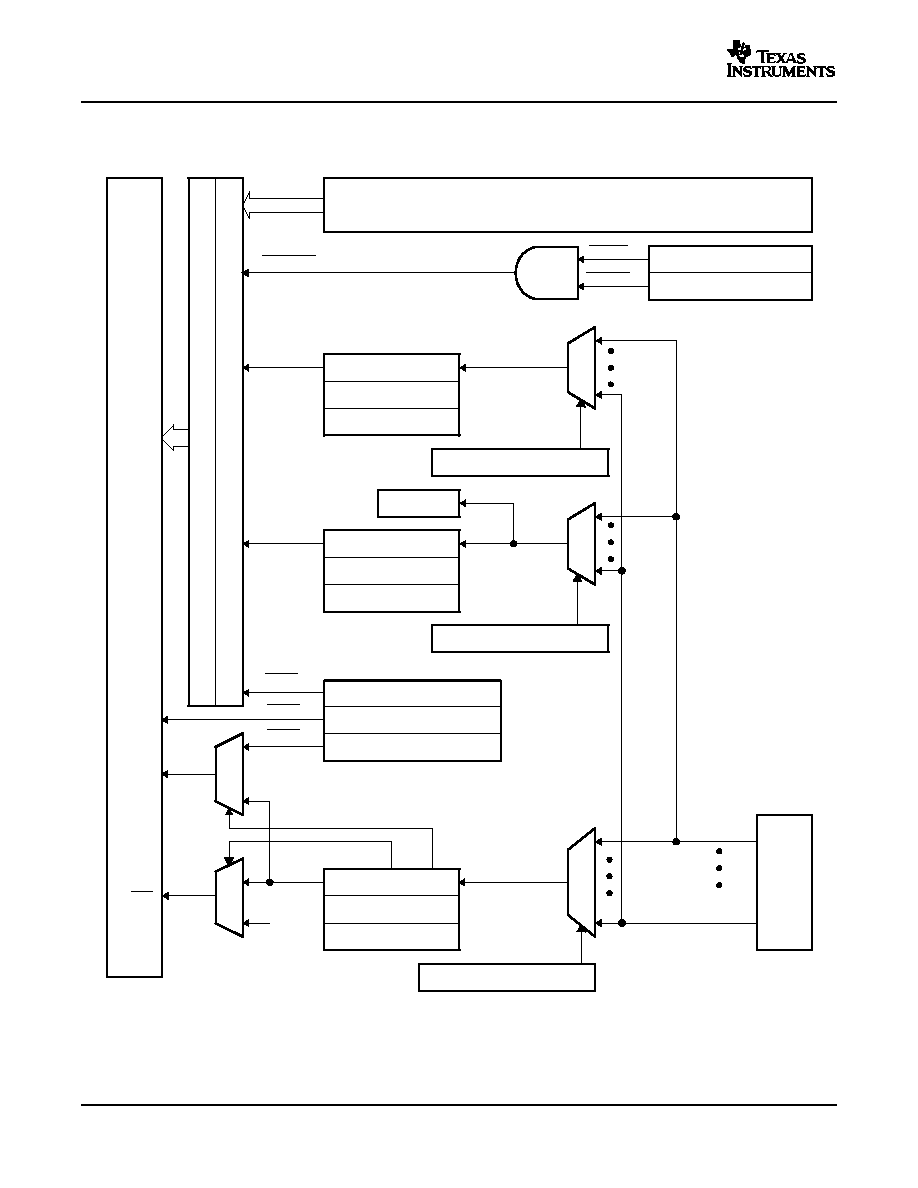
www.ti.com
3.5
Interrupts
XINT2
C28
CPU
CPU TIMER 2 (for TI/RTOS)
CPU TIMER 0
Watchdog
Peripherals
(SPI, SCI, I
2
C, eCAN, ePWM, eCAP, eQEP, ADC)
TINT0
Interrupt Control
XNMICR(15:0)
XINT1
Interrupt Control
XINT1
XINT1CR(15:0)
Interrupt Control
XINT2
XINT2CR(15:0)
GPIO
MUX
WDINT
INT1 to
INT12
INT13
INT14
NMI
XINT1CTR(15:0)
XINT2CTR(15:0)
XNMICTR(15:0)
CPU TIMER 1 (for TI)
TINT2
Low Power Modes
LPMINT
WAKEINT
TINT1
int13_select
XNMI_XINT13
GPIO0.int
GPIO31.int
ADC
XINT2SOC
GPIOXINT1SEL(4:0)
GPIOXINT2SEL(4:0)
GPIOXNMISEL(4:0)
nmi_select
1
MUX
MUX
PIE
96 Interrupts
MUX
MUX
MUX
TMS320F2809, TMS320F2808, TMS320F2806
TMS320F2802, TMS320F2801, UCD9501
TMS320C2802, TMS320C2801 Digital Signal Processors
SPRS230G ≠ OCTOBER 2003 ≠ REVISED FEBRUARY 2006
Figure 3-6
shows how the various interrupt sources are multiplexed within the 280x devices.
Figure 3-6. External and PIE Interrupt Sources
Eight PIE block interrupts are grouped into one CPU interrupt. In total, 12 CPU interrupt groups, with 8
interrupts per group equals 96 possible interrupts. On the 280x, 43 of these are used by peripherals as
shown in
Table 3-11
.
42
Functional Overview
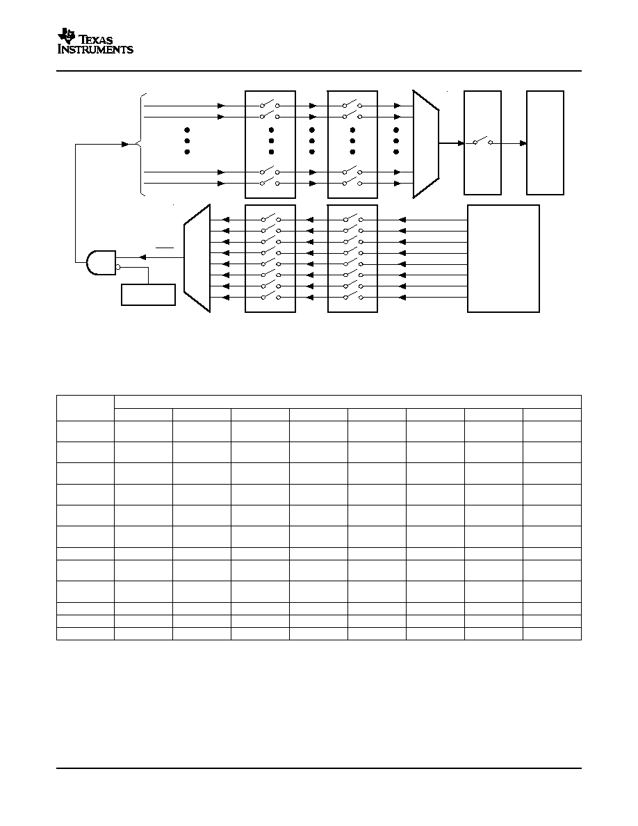
www.ti.com
INT12
MUX
INT11
INT2
INT1
CPU
(Enable)
(Flag)
INTx
INTx.8
PIEIERx(8:1)
PIEIFRx(8:1)
MUX
INTx.7
INTx.6
INTx.5
INTx.4
INTx.3
INTx.2
INTx.1
From
Peripherals or
External
Interrupts
(Enable)
(Flag)
IER(12:1)
IFR(12:1)
Global
Enable
INTM
1
0
PIEACKx
(Enable/Flag)
TMS320F2809, TMS320F2808, TMS320F2806
TMS320F2802, TMS320F2801, UCD9501
TMS320C2802, TMS320C2801 Digital Signal Processors
SPRS230G ≠ OCTOBER 2003 ≠ REVISED FEBRUARY 2006
Figure 3-7. Multiplexing of Interrupts Using the PIE Block
Table 3-11. PIE Peripheral Interrupts
(1)
PIE INTERRUPTS
CPU
INTERRUPTS
INTx.8
INTx.7
INTx.6
INTx.5
INTx.4
INTx.3
INTx.2
INTx.1
WAKEINT
TINT0
ADCINT
SEQ2INT
SEQ1INT
INT1
XINT2
XINT1
reserved
(LPM/WD)
(TIMER 0)
(ADC)
(ADC)
(ADC)
EPWM6_TZINT
EPWM5_TZINT
EPWM4_TZINT
EPWM3_TZINT
EPWM2_TZINT
EPWM1_TZINT
INT2
reserved
reserved
(ePWM6)
(ePWM5)
(ePWM4)
(ePWM3)
(ePWM2)
(ePWM1)
EPWM6_INT
EPWM5_INT
EPWM4_INT
EPWM3_INT
EPWM2_INT
EPWM1_INT
INT3
reserved
reserved
(ePWM6)
(ePWM5)
(ePWM4)
(ePWM3)
(ePWM2)
(ePWM1)
ECAP4_INT
ECAP3_INT
ECAP2_INT
ECAP1_INT
INT4
reserved
reserved
reserved
reserved
(eCAP4)
(eCAP3)
(eCAP2)
(eCAP1)
EQEP2_INT
EQEP1_INT
INT5
reserved
reserved
reserved
reserved
reserved
reserved
(eQEP2)
(eQEP1)
SPITXINTD
SPIRXINTD
SPITXINTC
SPIRXINTC
SPITXINTB
SPIRXINTB
SPITXINTA
SPIRXINTA
INT6
(SPI-D)
(SPI-D)
(SPI-C)
(SPI-C)
(SPI-B)
(SPI-B)
(SPI-A)
(SPI-A)
INT7
reserved
reserved
reserved
reserved
reserved
reserved
reserved
reserved
I2CINT2A
I2CINT1A
INT8
reserved
reserved
reserved
reserved
reserved
reserved
(I2C-A)
(I2C-A)
ECAN1_INTB
ECAN0_INTB
ECAN1_INTA
ECAN0_INTA
SCITXINTB
SCIRXINTB
SCITXINTA
SCIRXINTA
INT9
(CAN-B)
(CAN-B)
(CAN-A)
(CAN-A)
(SCI-B)
(SCI-B)
(SCI-A)
(SCI-A)
INT10
reserved
reserved
reserved
reserved
reserved
reserved
reserved
reserved
INT11
reserved
reserved
reserved
reserved
reserved
reserved
reserved
reserved
INT12
reserved
reserved
reserved
reserved
reserved
reserved
reserved
reserved
(1)
Out of the 96 possible interrupts, 43 interrupts are currently used. The remaining interrupts are reserved for future devices. These
interrupts can be used as software interrupts if they are enabled at the PIEIFRx level, provided none of the interrupts within the group is
being used by a peripheral. Otherwise, interrupts coming in from peripherals may be lost by accidentally clearing their flag while
modifying the PIEIFR. To summarize, there are two safe cases when the reserved interrupts could be used as software interrupts:
1) No peripheral within the group is asserting interrupts.
2) No peripheral interrupts are assigned to the group (example PIE group 12).
Functional Overview
43
www.ti.com
3.5.1
External Interrupts
TMS320F2809, TMS320F2808, TMS320F2806
TMS320F2802, TMS320F2801, UCD9501
TMS320C2802, TMS320C2801 Digital Signal Processors
SPRS230G ≠ OCTOBER 2003 ≠ REVISED FEBRUARY 2006
Table 3-12. PIE Configuration and Control Registers
NAME
ADDRESS
SIZE (X16)
DESCRIPTION
(1)
PIECTRL
0x0CE0
1
PIE, Control Register
PIEACK
0x0CE1
1
PIE, Acknowledge Register
PIEIER1
0x0CE2
1
PIE, INT1 Group Enable Register
PIEIFR1
0x0CE3
1
PIE, INT1 Group Flag Register
PIEIER2
0x0CE4
1
PIE, INT2 Group Enable Register
PIEIFR2
0x0CE5
1
PIE, INT2 Group Flag Register
PIEIER3
0x0CE6
1
PIE, INT3 Group Enable Register
PIEIFR3
0x0CE7
1
PIE, INT3 Group Flag Register
PIEIER4
0x0CE8
1
PIE, INT4 Group Enable Register
PIEIFR4
0x0CE9
1
PIE, INT4 Group Flag Register
PIEIER5
0x0CEA
1
PIE, INT5 Group Enable Register
PIEIFR5
0x0CEB
1
PIE, INT5 Group Flag Register
PIEIER6
0x0CEC
1
PIE, INT6 Group Enable Register
PIEIFR6
0x0CED
1
PIE, INT6 Group Flag Register
PIEIER7
0x0CEE
1
PIE, INT7 Group Enable Register
PIEIFR7
0x0CEF
1
PIE, INT7 Group Flag Register
PIEIER8
0x0CF0
1
PIE, INT8 Group Enable Register
PIEIFR8
0x0CF1
1
PIE, INT8 Group Flag Register
PIEIER9
0x0CF2
1
PIE, INT9 Group Enable Register
PIEIFR9
0x0CF3
1
PIE, INT9 Group Flag Register
PIEIER10
0x0CF4
1
PIE, INT10 Group Enable Register
PIEIFR10
0x0CF5
1
PIE, INT10 Group Flag Register
PIEIER11
0x0CF6
1
PIE, INT11 Group Enable Register
PIEIFR11
0x0CF7
1
PIE, INT11 Group Flag Register
PIEIER12
0x0CF8
1
PIE, INT12 Group Enable Register
PIEIFR12
0x0CF9
1
PIE, INT12 Group Flag Register
Reserved
0x0CFA
6
Reserved
0x0CFF
(1)
The PIE configuration and control registers are not protected by EALLOW mode. The PIE vector table
is protected.
Table 3-13. External Interrupt Registers
NAME
ADDRESS
SIZE (x16)
DESCRIPTION
XINT1CR
0x7070
1
XINT1 control register
XINT2CR
0x7071
1
XINT2 control register
0x7072
reserved
5
0x7076
XNMICR
0x7077
1
XNMI control register
XINT1CTR
0x7078
1
XINT1 counter register
XINT2CTR
0x7079
1
XINT2 counter register
0x707A
reserved
5
0x707E
XNMICTR
0x707F
1
XNMI counter register
Functional Overview
44
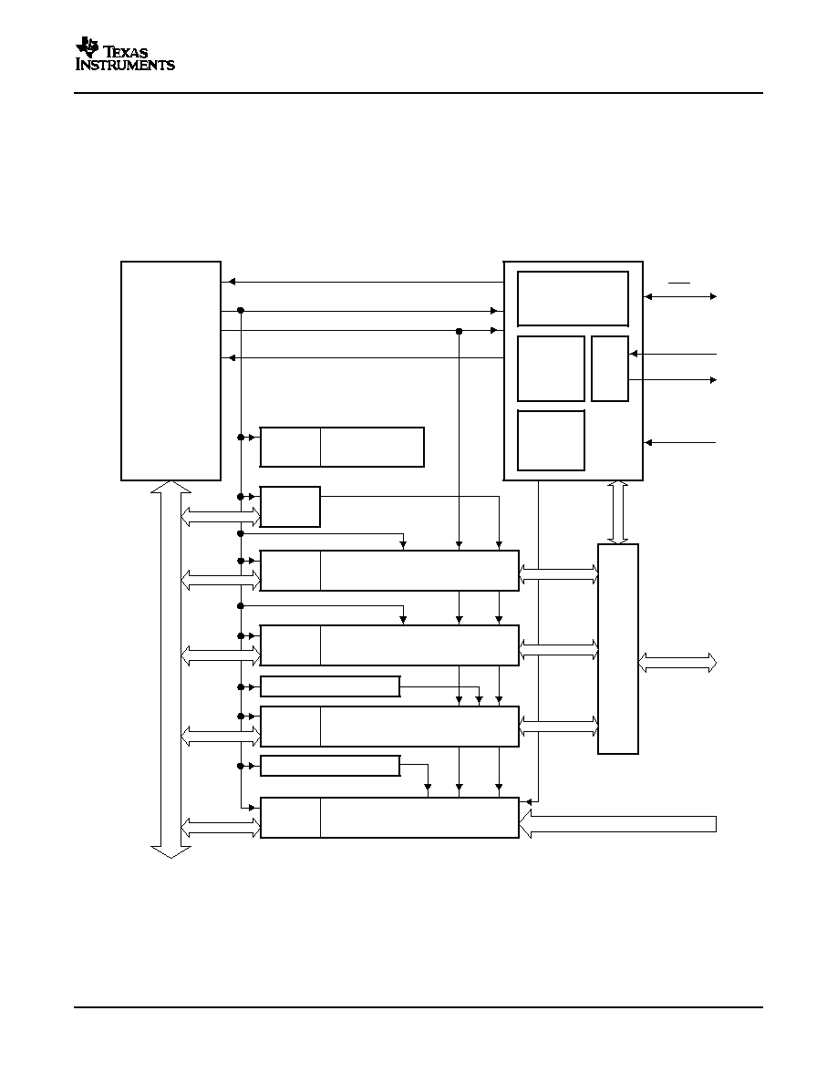
www.ti.com
3.6
System Control
PLL
X1
X2
Power
Modes
Control
Watchdog
Block
28x
CPU
Peripheral Bus
Low-Speed Peripherals
SCI-A/B, SPI-A/B/C/D
Peripheral
Registers
High-Speed Prescaler
Low-Speed Prescaler
Clock Enables
GPIO
MUX
System
Control
Registers
XCLKIN
ADC
Registers
12-Bit ADC
16 ADC inputs
LSPCLK
I/O
Peripheral Reset
SYSCLKOUT
(A)
XRS
Reset
GPIOs
Peripheral
Registers
I/O
OSC
CLKIN
(A)
HSPCLK
eCAN-A/B
I
2
C-A
Peripheral
Registers
I/O
ePWM 1/2/3/4/5/6
eCAP 1/2/3/4 eQEP 1/2
Peripheral
Registers
CPU
Timers
TMS320F2809, TMS320F2808, TMS320F2806
TMS320F2802, TMS320F2801, UCD9501
TMS320C2802, TMS320C2801 Digital Signal Processors
SPRS230G ≠ OCTOBER 2003 ≠ REVISED FEBRUARY 2006
Each external interrupt can be enabled/disabled or qualified using positive, negative, or both positive and
negative edge. For more information, see the TMS320x280x System Control and Interrupts Reference
Guide (literature number SPRU712).
This section describes the 280x oscillator, PLL and clocking mechanisms, the watchdog function and the
low power modes.
Figure 3-8
shows the various clock and reset domains in the 280x devices that will be
discussed.
A.
CLKIN is the clock into the CPU. It is passed out of the CPU as SYSCLKOUT (that is, CLKIN is the same frequency
as SYSCLKOUT).
Figure 3-8. Clock and Reset Domains
Functional Overview
45
www.ti.com
TMS320F2809, TMS320F2808, TMS320F2806
TMS320F2802, TMS320F2801, UCD9501
TMS320C2802, TMS320C2801 Digital Signal Processors
SPRS230G ≠ OCTOBER 2003 ≠ REVISED FEBRUARY 2006
The PLL, clocking, watchdog and low-power modes, are controlled by the registers listed in
Table 3-14
.
Table 3-14. PLL, Clocking, Watchdog, and Low-Power Mode Registers
(1)
NAME
ADDRESS
SIZE (x16)
DESCRIPTION
XCLK
0x7010
1
XCLKOUT Pin Control, X1 and XCLKIN Status Register
PLLSTS
0x7011
1
PLL Status Register
0x7012
reserved
8
0x7019
HISPCP
0x701A
1
High-Speed Peripheral Clock Prescaler Register (for HSPCLK)
LOSPCP
0x701B
1
Low-Speed Peripheral Clock Prescaler Register (for LSPCLK)
PCLKCR0
0x701C
1
Peripheral Clock Control Register 0
PCLKCR1
0x701D
1
Peripheral Clock Control Register 1
LPMCR0
0x701E
1
Low Power Mode Control Register 0
0x701F
reserved
1
0x7020
PLLCR
0x7021
1
PLL Control Register
SCSR
0x7022
1
System Control and Status Register
WDCNTR
0x7023
1
Watchdog Counter Register
reserved
0x7024
1
WDKEY
0x7025
1
Watchdog Reset Key Register
0x7026
reserved
3
0x7028
WDCR
0x7029
1
Watchdog Control Register
0x702A
reserved
6
0x702F
(1)
All of the registers in this table are EALLOW protected.
Functional Overview
46
www.ti.com
3.6.1
OSC and PLL Block
X1
XCLKIN
(3.3-V clock input)
On chip
oscillator
X2
xor
PLLSTS[OSCOFF]
OSCCLK
PLL
VCOCLK
4-bit PLL Select (PLLCR)
OSCCLK or
VCOCLK
CLKIN
OSCCLK
0
PLLSTS[PLLOFF]
n
n
0
/2
PLLSTS[CLKINDIV]
External Clock Signal
(Toggling 0 -V
DDIO
)
XCLKIN
X2
NC
X1
External Clock Signal
(Toggling 0 -V
DD
)
XCLKIN
X2
NC
X1
C
L1
X2
X1
Crystal
C
L2
XCLKIN
TMS320F2809, TMS320F2808, TMS320F2806
TMS320F2802, TMS320F2801, UCD9501
TMS320C2802, TMS320C2801 Digital Signal Processors
SPRS230G ≠ OCTOBER 2003 ≠ REVISED FEBRUARY 2006
Figure 3-9
shows the OSC and PLL block on the 280x.
Figure 3-9. OSC and PLL Block Diagram
The on-chip oscillator circuit enables a crystal/resonator to be attached to the 280x devices using the X1
and X2 pins. If the on-chip oscillator is not used, an external oscillator can be used in either one of the
following configurations:
1. A 3.3-V external oscillator can be directly connected to the XCLKIN pin. The X2 pin should be left
unconnected and the X1 pin tied low. The logic-high level in this case should not exceed V
DDIO
.
2. A 1.8-V external oscillator can be directly connected to the X1 pin. The X2 pin should be left
unconnected and the XCLKIN pin tied low. The logic-high level in this case should not exceed V
DD
.
The three possible input-clock configurations are shown in
Figure 3-10
through
Figure 3-12
Figure 3-10. Using a 3.3-V External Oscillator
Figure 3-11. Using a 1.8-V External Oscillator
Figure 3-12. Using the Internal Oscillator
Functional Overview
47

www.ti.com
TMS320F2809, TMS320F2808, TMS320F2806
TMS320F2802, TMS320F2801, UCD9501
TMS320C2802, TMS320C2801 Digital Signal Processors
SPRS230G ≠ OCTOBER 2003 ≠ REVISED FEBRUARY 2006
3.6.1.1
External Reference Oscillator Clock Option
The typical specifications for the external quartz crystal for a frequency of 20 MHz are listed below:
∑
Fundamental mode, parallel resonant
∑
C
L
(load capacitance) = 12 pF
∑
C
L1
= C
L2
= 24 pF
∑
C
shunt
= 6 pF
∑
ESR range = 30 to 60
TI recommends that customers have the resonator/crystal vendor characterize the operation of their
device with the DSP chip. The resonator/crystal vendor has the equipment and expertise to tune the tank
circuit. The vendor can also advise the customer regarding the proper tank component values that will
produce proper start up and stability over the entire operating range.
3.6.1.2
PLL-Based Clock Module
The 280x devices have an on-chip, PLL-based clock module. This module provides all the necessary
clocking signals for the device, as well as control for low-power mode entry. The PLL has a 4-bit ratio
control PLLCR[DIV] to select different CPU clock rates. The watchdog module should be disabled before
writing to the PLLCR register. It can be re-enabled (if need be) after the PLL module has stabilized, which
takes 131072 OSCCLK cycles.
Table 3-15. PLLCR Register Bit Definitions
SYSCLKOUT
PLLCR[DIV]
(1)
PLLSTS[CLKINDIV]
(CLKIN)
(2)
0000 (PLL bypass)
0
OSCCLK/2
0000 (PLL bypass)
1
OSCCLK
0001
0
(OSCCLK*1)/2
0010
0
(OSCCLK*2)/2
0011
0
(OSCCLK*3)/2
0100
0
(OSCCLK*4)/2
0101
0
(OSCCLK*5)/2
0110
0
(OSCCLK*6)/2
0111
0
(OSCCLK*7)/2
1000
0
(OSCCLK*8)/2
1001
0
(OSCCLK*9)/2
1010
0
(OSCCLK*10)/2
1011-1111
0
reserved
(1)
This register is EALLOW protected.
(2)
CLKIN is the input clock to the CPU. SYSCLKOUT is the output
clock from the CPU. The frequency of SYSCLKOUT is the same as
CLKIN.
CAUTION
PLLSTS[CLKINDIV] can be set to 1 only if PLLCR is 0x0000. PLLCR should not be
changed once PLLSTS[CLKINDIV] is set.
The PLL-based clock module provides two modes of operation:
∑
Crystal-operation - This mode allows the use of an external crystal/resonator to provide the time base
to the device.
∑
External clock source operation - This mode allows the internal oscillator to be bypassed. The device
clocks are generated from an external clock source input on the X1 or the XCLKIN pin.
Functional Overview
48
www.ti.com
3.6.2
Watchdog Block
TMS320F2809, TMS320F2808, TMS320F2806
TMS320F2802, TMS320F2801, UCD9501
TMS320C2802, TMS320C2801 Digital Signal Processors
SPRS230G ≠ OCTOBER 2003 ≠ REVISED FEBRUARY 2006
Table 3-16. Possible PLL Configuration Modes
SYSCLKOUT
PLL MODE
REMARKS
PLLSTS[CLKINDIV]
(CLKIN)
Invoked by the user setting the PLLOFF bit in the PLLSTS register. The PLL block
0
OSCCLK/2
is disabled in this mode. This can be useful to reduce system noise and for low
PLL Off
power operation. The PLLCR register must first be set to 0x0000 (PLL Bypass)
1
OSCCLK
before entering this mode. The CPU clock (CLKIN) is derived directly from the
input clock on either X1/X2, X1 or XCLKIN.
PLL Bypass is the default PLL configuration upon power-up or after an external
0
OSCCLK/2
reset (XRS). This mode is selected when the PLLCR register is set to 0x0000 or
PLL Bypass
while the PLL locks to a new frequency after the PLLCR register has been
1
OSCCLK
modified. In this mode, the PLL itself is bypassed but the PLL is not turned off.
Achieved by writing a non-zero value n into the PLLCR register. Upon writing to the
PLL Enable
0
OSCCLK*n/2
PLLCR the device will switch to PLL Bypass mode until the PLL locks.
3.6.1.3
Loss of Input Clock
In PLL-enabled and PLL-bypass mode, if the input clock OSCCLK is removed or absent, the PLL will still
issue a "limp-mode" clock. The limp-mode clock continues to clock the CPU and peripherals at a typical
frequency of 1-5 MHz. Limp mode is not specified to work from power-up, only after input clocks have
been present initially. In PLL bypass mode, the limp mode clock from the PLL is automatically routed to
the CPU if the input clock is removed or absent.
Normally, when the input clocks are present, the watchdog counter decrements to initiate a watchdog
reset or WDINT interrupt. However, when the external input clock fails, the watchdog counter stops
decrementing (i.e., the watchdog counter does not change with the limp-mode clock). In addition to this,
the device will be reset and the "Missing Clock Status" (MCLKSTS) bit will be set. These conditions could
be used by the application firmware to detect the input clock failure and initiate necessary shut-down
procedure for the system.
NOTE
Applications in which the correct CPU operating frequency is absolutely critical should
implement a mechanism by which the DSP will be held in reset, should the input clocks
ever fail. For example, an R-C circuit may be used to trigger the XRS pin of the DSP,
should the capacitor ever get fully charged. An I/O pin may be used to discharge the
capacitor on a periodic basis to prevent it from getting fully charged. Such a circuit would
also help in detecting failure of the flash memory and the V
DD3VFL
rail.
The watchdog block on the 280x is similar to the one used on the 240x and 281x devices. The watchdog
module generates an output pulse, 512 oscillator clocks wide (OSCCLK), whenever the 8-bit watchdog up
counter has reached its maximum value. To prevent this, the user disables the counter or the software
must periodically write a 0x55 + 0xAA sequence into the watchdog key register which will reset the
watchdog counter.
Figure 3-13
shows the various functional blocks within the watchdog module.
Functional Overview
49
www.ti.com
/512
OSCCLK
WDCR (WDPS(2:0))
WDCLK
WDCNTR(7:0)
WDKEY(7:0)
Good Key
1
0
1
WDCR (WDCHK(2:0))
Bad
WDCHK
Key
WDCR (WDDIS)
Clear Counter
SCSR (WDENINT)
Watchdog
Prescaler
Generate
Output Pulse
(512 OSCCLKs)
8-Bit
Watchdog
Counter
CLR
WDRST
WDINT
Watchdog
55 + AA
Key Detector
XRS
Core-reset
WDRST
(A)
Internal
Pullup
TMS320F2809, TMS320F2808, TMS320F2806
TMS320F2802, TMS320F2801, UCD9501
TMS320C2802, TMS320C2801 Digital Signal Processors
SPRS230G ≠ OCTOBER 2003 ≠ REVISED FEBRUARY 2006
A.
The WDRST signal is driven low for 512 OSCCLK cycles.
Figure 3-13. Watchdog Module
The WDINT signal enables the watchdog to be used as a wakeup from IDLE/STANDBY mode.
In STANDBY mode, all peripherals are turned off on the device. The only peripheral that remains
functional is the watchdog. The WATCHDOG module will run off OSCCLK. The WDINT signal is fed to the
LPM block so that it can wake the device from STANDBY (if enabled). See Section
Section 3.7
,
Low-Power Modes Block, for more details.
In IDLE mode, the WDINT signal can generate an interrupt to the CPU, via the PIE, to take the CPU out of
IDLE mode.
In HALT mode, this feature cannot be used because the oscillator (and PLL) are turned off and hence so
is the WATCHDOG.
Functional Overview
50
www.ti.com
3.7
Low-Power Modes Block
TMS320F2809, TMS320F2808, TMS320F2806
TMS320F2802, TMS320F2801, UCD9501
TMS320C2802, TMS320C2801 Digital Signal Processors
SPRS230G ≠ OCTOBER 2003 ≠ REVISED FEBRUARY 2006
The low-power modes on the 280x are similar to the 240x devices.
Table 3-17
summarizes the various
modes.
Table 3-17. Low-Power Modes
MODE
LPMCR0(1:0)
OSCCLK
CLKIN
SYSCLKOUT
EXIT
(1)
XRS, Watchdog interrupt, any enabled
IDLE
00
On
On
On
(2)
interrupt, XNMI
On
XRS, Watchdog interrupt, GPIO Port A
STANDBY
01
Off
Off
(watchdog still running)
signal, debugger
(3)
, XNMI
Off
XRS, GPIO Port A signal, XNMI,
HALT
1X
(oscillator and PLL turned off,
Off
Off
debugger
(3)
watchdog not functional)
(1)
The Exit column lists which signals or under what conditions the low power mode will be exited. A low signal, on any of the signals, will
exit the low power condition. This signal must be kept low long enough for an interrupt to be recognized by the device. Otherwise the
IDLE mode will not be exited and the device will go back into the indicated low power mode.
(2)
The IDLE mode on the C28x behaves differently than on the 24x/240x. On the C28x, the clock output from the CPU (SYSCLKOUT) is
still functional while on the 24x/240x the clock is turned off.
(3)
On the C28x, the JTAG port can still function even if the CPU clock (CLKIN) is turned off.
The various low-power modes operate as follows:
IDLE Mode:
This mode is exited by any enabled interrupt or an XNMI that is recognized by
the processor. The LPM block performs no tasks during this mode as long as the
LPMCR0(LPM) bits are set to 0,0.
STANDBY Mode:
Any GPIO port A signal (GPIO[31:0]) can wake the device from STANDBY
mode. The user must select which signal(s) will wake the device in the
GPIOLPMSEL register. The selected signal(s) are also qualified by the OSCCLK
before waking the device. The number of OSCCLKs is specified in the LPMCR0
register.
HALT Mode:
Only the XRS and any GPIO port A signal (GPIO[31:0]) can wake the device
from HALT mode. The user selects the signal in the GPIOLPMSEL register.
NOTE
The low-power modes do not affect the state of the output pins (PWM pins included).
They will be in whatever state the code left them in when the IDLE instruction was
executed. See the TMS320x280x System Control and Interrupts Reference Guide
(literature number SPRU712) for more details.
Functional Overview
51
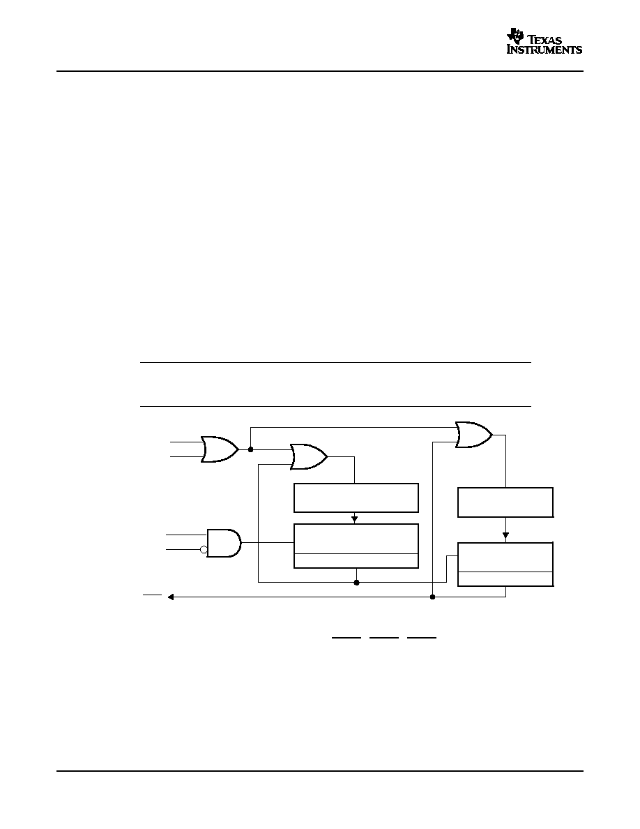
www.ti.com
4
Peripherals
4.1
32-Bit CPU-Timers 0/1/2
Borrow
Reset
Timer Reload
SYSCLKOUT
TCR.4
(Timer Start Status)
TINT
16-Bit Timer Divide-Down
TDDRH:TDDR
32-Bit Timer Period
PRDH:PRD
32-Bit Counter
TIMH:TIM
16-Bit Prescale Counter
PSCH:PSC
Borrow
TMS320F2809, TMS320F2808, TMS320F2806
TMS320F2802, TMS320F2801, UCD9501
TMS320C2802, TMS320C2801 Digital Signal Processors
SPRS230G ≠ OCTOBER 2003 ≠ REVISED FEBRUARY 2006
The integrated peripherals of the 280x are described in the following subsections:
∑
Three 32-bit CPU-Timers
∑
Up to six enhanced PWM modules (ePWM1, ePWM2, ePWM3, ePWM4, ePWM5, ePWM6)
∑
Up to four enhanced capture modules (eCAP1, eCAP2, eCAP3, eCAP4)
∑
Up to two enhanced QEP modules (eQEP1, eQEP2)
∑
Enhanced analog-to-digital converter (ADC) module
∑
Up to two enhanced controller area network (eCAN) modules (eCAN-A, eCAN-B)
∑
Up to two serial communications interface modules (SCI-A, SCI-B)
∑
Up to four serial peripheral interface (SPI) modules (SPI-A, SPI-B, SPI-C, SPI-D)
∑
Inter-integrated circuit module (I
2
C)
∑
Digital I/O and shared pin functions
There are three 32-bit CPU-timers on the 280x devices (CPU-TIMER0/1/2).
CPU-Timer 1 is reserved for TI system functions and Timer 2 is reserved for DSP/BIOSTM. CPU-Timer 0
can be used in user applications. These timers are different from the timers that are present in the ePWM
modules.
NOTE
NOTE: If the application is not using DSP/BIOS, then CPU-Timer 2 can be used in the
application.
Figure 4-1. CPU-Timers
In the 280x devices, the timer interrupt signals (TINT0, TINT1, TINT2) are connected as shown in
Figure 4-2
.
52
Peripherals
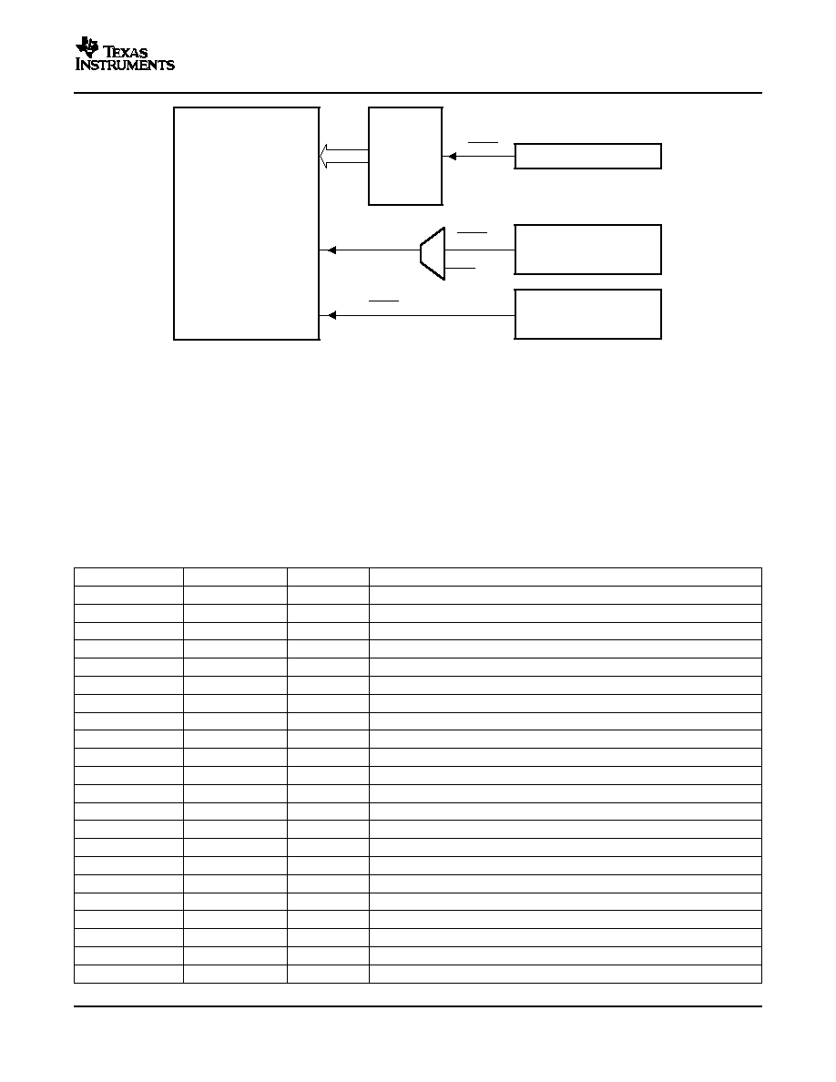
www.ti.com
INT1
to
INT12
INT14
C28x
TINT2
TINT0
PIE
CPU-TIMER 0
CPU-TIMER 2
(Reserved for
DSP/BIOS)
INT13
TINT1
CPU-TIMER 1
(Reserved for TI
system functions)
XINT13
TMS320F2809, TMS320F2808, TMS320F2806
TMS320F2802, TMS320F2801, UCD9501
TMS320C2802, TMS320C2801 Digital Signal Processors
SPRS230G ≠ OCTOBER 2003 ≠ REVISED FEBRUARY 2006
A.
The timer registers are connected to the memory bus of the C28x processor.
B.
The timing of the timers is synchronized to SYSCLKOUT of the processor clock.
C.
While TIMER1 is reserved, INT13 is not reserved and the user can use XINT13 connected to INT13.
Figure 4-2. CPU-Timer Interrupt Signals and Output Signal
The general operation of the timer is as follows: The 32-bit counter register "TIMH:TIM" is loaded with the
value in the period register "PRDH:PRD". The counter register decrements at the SYSCLKOUT rate of the
C28x. When the counter reaches 0, a timer interrupt output signal generates an interrupt pulse. The
registers listed in
Table 4-1
are used to configure the timers. For more information, see the TMS320x280x
System Control and Interrupts Reference Guide (literature number SPRU712).
Table 4-1. CPU-Timers 0, 1, 2 Configuration and Control Registers
NAME
ADDRESS
SIZE (x16)
DESCRIPTION
TIMER0TIM
0x0C00
1
CPU-Timer 0, Counter Register
TIMER0TIMH
0x0C01
1
CPU-Timer 0, Counter Register High
TIMER0PRD
0x0C02
1
CPU-Timer 0, Period Register
TIMER0PRDH
0x0C03
1
CPU-Timer 0, Period Register High
TIMER0TCR
0x0C04
1
CPU-Timer 0, Control Register
reserved
0x0C05
1
TIMER0TPR
0x0C06
1
CPU-Timer 0, Prescale Register
TIMER0TPRH
0x0C07
1
CPU-Timer 0, Prescale Register High
TIMER1TIM
0x0C08
1
CPU-Timer 1, Counter Register
TIMER1TIMH
0x0C09
1
CPU-Timer 1, Counter Register High
TIMER1PRD
0x0C0A
1
CPU-Timer 1, Period Register
TIMER1PRDH
0x0C0B
1
CPU-Timer 1, Period Register High
TIMER1TCR
0x0C0C
1
CPU-Timer 1, Control Register
reserved
0x0C0D
1
TIMER1TPR
0x0C0E
1
CPU-Timer 1, Prescale Register
TIMER1TPRH
0x0C0F
1
CPU-Timer 1, Prescale Register High
TIMER2TIM
0x0C10
1
CPU-Timer 2, Counter Register
TIMER2TIMH
0x0C11
1
CPU-Timer 2, Counter Register High
TIMER2PRD
0x0C12
1
CPU-Timer 2, Period Register
TIMER2PRDH
0x0C13
1
CPU-Timer 2, Period Register High
TIMER2TCR
0x0C14
1
CPU-Timer 2, Control Register
reserved
0x0C15
1
Peripherals
53
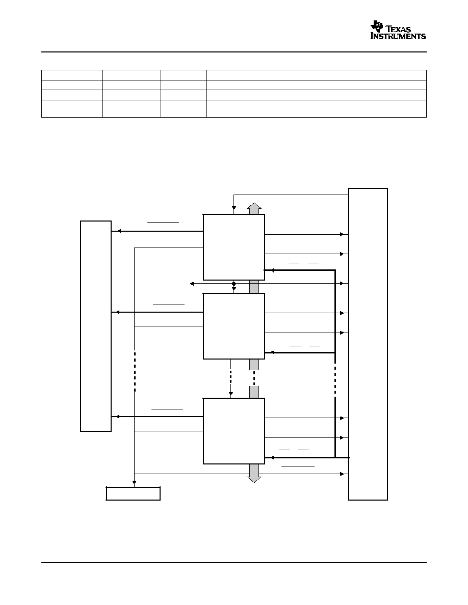
www.ti.com
4.2
Enhanced PWM Modules (ePWM1/2/3/4/5/6)
PIE
TZ1 to TZ6
Peripheral Bus
ePWM1 module
ePWM2 module
ePWMx module
SYNCI
SYNCI
SYNCO
SYNCI
SYNCO
ADC
GPIO
MUX
xSYNCI
xSYNCO
ADCSOCx0
EPWMxA
EPWMxB
EPWM2A
EPWM2B
EPWM1A
EPWM1B
EPWM1INT
EPWM1SOC
EPWM2INT
EPWM2SOC
EPWMxINT
EPWMxSOC
to eCAP1
module
(sync in)
TZ1 to TZ6
TZ1 to TZ6
.
SYNCO
TMS320F2809, TMS320F2808, TMS320F2806
TMS320F2802, TMS320F2801, UCD9501
TMS320C2802, TMS320C2801 Digital Signal Processors
SPRS230G ≠ OCTOBER 2003 ≠ REVISED FEBRUARY 2006
Table 4-1. CPU-Timers 0, 1, 2 Configuration and Control Registers (continued)
NAME
ADDRESS
SIZE (x16)
DESCRIPTION
TIMER2TPR
0x0C16
1
CPU-Timer 2, Prescale Register
TIMER2TPRH
0x0C17
1
CPU-Timer 2, Prescale Register High
0x0C18
reserved
40
0x0C3F
The 280x device contains up to six enhanced PWM Modules (ePWM).
Figure 4-3
shows a block diagram
of multiple ePWM modules. Figure 4-4 shows the signal interconnections with the ePWM. See the
TMS320x280x Enhanced Pulse Width Modulator (ePWM) Module Reference Guide (literature number
SPRU791) for more details.
Figure 4-3. Multiple PWM Modules in a 280x System
Table 4-2
shows the complete ePWM register set per module.
Peripherals
54

www.ti.com
TMS320F2809, TMS320F2808, TMS320F2806
TMS320F2802, TMS320F2801, UCD9501
TMS320C2802, TMS320C2801 Digital Signal Processors
SPRS230G ≠ OCTOBER 2003 ≠ REVISED FEBRUARY 2006
Table 4-2. ePWM Control and Status Registers
SIZE (x16) /
NAME
EPWM1
EPWM2
EPWM3
EPWM4
EPWM5
EPWM6
DESCRIPTION
#SHADOW
TBCTL
0x6800
0x6840
0x6880
0x68C0
0x6900
0x6940
1 / 0
Time Base Control Register
TBSTS
0x6801
0x6841
0x6881
0x68C1
0x6901
0x6941
1 / 0
Time Base Status Register
TBPHSHR
0x6802
0x6842
0x6882
0x68C2
N/A
N/A
1 / 0
Time Base Phase HRPWM Register
TBPHS
0x6803
0x6843
0x6883
0x68C3
0x6903
0x6943
1 / 0
Time Base Phase Register
TBCNT
0x6804
0x6844
0x6884
0x68C4
0x6904
0x6944
1 / 0
Time Base Counter Register
TBPRD
0x6805
0x6845
0x6885
0x68C5
0x6905
0x6945
1 / 1
Time Base Period Register Set
CMPCTL
0x6807
0x6847
0x6887
0x68C7
0x6907
0x6947
1 / 0
Counter Compare Control Register
CMPAHR
0x6808
0x6848
0x6888
0x68C8
N/A
N/A
1 / 1
Time Base Compare A HRPWM Register
CMPA
0x6809
0x6849
0x6889
0x68C9
0x6909
0x6949
1 / 1
Counter Compare A Register Set
CMPB
0x680A
0x684A
0x688A
0x68CA
0x690A
0x694A
1 / 1
Counter Compare B Register Set
AQCTLA
0x680B
0x684B
0x688B
0x68CB
0x690B
0x694B
1 / 0
Action Qualifier Control Register For Output A
AQCTLB
0x680C
0x684C
0x688C
0x68CC
0x690C
0x694C
1 / 0
Action Qualifier Control Register For Output B
AQSFRC
0x680D
0x684D
0x688D
0x68CD
0x690D
0x694D
1 / 0
Action Qualifier Software Force Register
AQCSFRC
0x680E
0x684E
0x688E
0x68CE
0x690E
0x694E
1 / 1
Action Qualifier Continuous S/W Force Register Set
DBCTL
0x680F
0x684F
0x688F
0x68CF
0x690F
0x694F
1 / 1
Dead-Band Generator Control Register
DBRED
0x6810
0x6850
0x6890
0x68D0
0x6910
0x6950
1 / 0
Dead-Band Generator Rising Edge Delay Count Register
DBFED
0x6811
0x6851
0x6891
0x68D1
0x6911
0x6951
1 / 0
Dead-Band Generator Falling Edge Delay Count Register
TZSEL
0x6812
0x6852
0x6892
0x68D2
0x6912
0x6952
1 / 0
Trip Zone Select Register
(1)
TZCTL
0x6814
0x6854
0x6894
0x68D4
0x6914
0x6954
1 / 0
Trip Zone Control Register
(1)
TZEINT
0x6815
0x6855
0x6895
0x68D5
0x6915
0x6955
1 / 0
Trip Zone Enable Interrupt Register
(1)
TZFLG
0x6816
0x6856
0x6896
0x68D6
0x6916
0x6956
1 / 0
Trip Zone Flag Register
TZCLR
0x6817
0x6857
0x6897
0x68D7
0x6917
0x6957
1 / 0
Trip Zone Clear Register
(1)
TZFRC
0x6818
0x6858
0x6898
0x68D8
0x6918
0x6958
1 / 0
Trip Zone Force Register
(1)
ETSEL
0x6819
0x6859
0x6899
0x68D9
0x6919
0x6959
1 / 0
Event Trigger Selection Register
ETPS
0x681A
0x685A
0x689A
0x68DA
0x691A
0x695A
1 / 0
Event Trigger Prescale Register
ETFLG
0x681B
0x685B
0x689B
0x68DB
0x691B
0x695B
1 / 0
Event Trigger Flag Register
ETCLR
0x681C
0x685C
0x689C
0x68DC
0x691C
0x695C
1 / 0
Event Trigger Clear Register
ETFRC
0x681D
0x685D
0x689D
0x68DD
0x691D
0x695D
1 / 0
Event Trigger Force Register
PCCTL
0x681E
0x685E
0x689E
0x68DE
0x691E
0x695E
1 / 0
PWM Chopper Control Register
HRCNFG
0x6820
0x6860
0x68A0
0x68E0
N/A
N/A
1 / 0
HRPWM Configuration Register
(1)
Registers that are EALLOW protected.
Peripherals
55
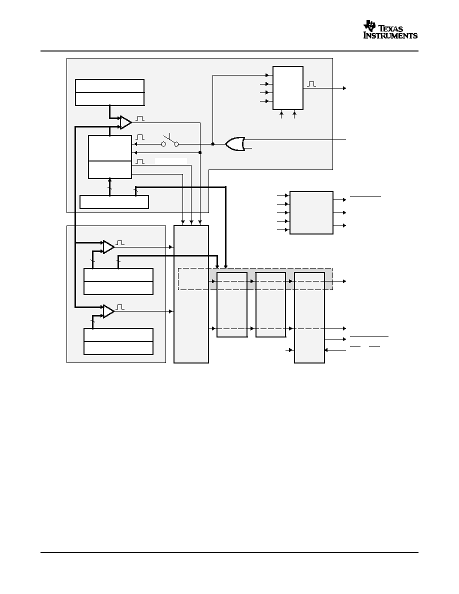
www.ti.com
CTR=PRD
TBPRD shadow (16)
TBPRD active (16)
Counter
up/down
(16 bit)
TBCNT
active (16)
TBCTL[CNTLDE]
TBCTL[SWFSYNC]
(software forced sync)
EPWMxSYNCI
CTR=ZERO
CTR_Dir
CTR=CMPB
Disabled
Sync
in/out
select
Mux
TBCTL[SYNCOSEL]
EPWMxSYNCO
TBPHS active (24)
16
8
TBPHSHR (8)
Phase
control
Time-base (TB)
CTR=CMPA
CMPA active (24)
16
CMPA shadow (24)
Action
qualifier
(AQ)
8
16
Counter compare (CC)
CMPB active (16)
CTR=CMPB
CMPB shadow (16)
CMPAHR (8)
EPWMA
EPWMB
Dead
band
(DB)
(PC)
chopper
PWM
zone
(TZ)
Trip
CTR = ZERO
EPWMxAO
EPWMxBO
EPWMxTZINT
TZ1 to TZ6
HiRes PWM (HRPWM)
CTR = PRD
CTR = ZERO
CTR = CMPB
CTR = CMPA
CTR_Dir
Event
trigger
and
interrupt
(ET)
EPWMxINT
EPWMxSOCA
EPWMxSOCB
CTR=ZERO
4.3
Hi-Resolution PWM (HRPWM)
TMS320F2809, TMS320F2808, TMS320F2806
TMS320F2802, TMS320F2801, UCD9501
TMS320C2802, TMS320C2801 Digital Signal Processors
SPRS230G ≠ OCTOBER 2003 ≠ REVISED FEBRUARY 2006
Figure 4-4. ePWM Sub-Modules Showing Critical Internal Signal Interconnections
The HRPWM module offers PWM resolution (time granularity) which is significantly better than what can
be achieved using conventionally derived digital PWM methods. The key points for the HRPWM module
are:
∑
Significantly extends the time resolution capabilities of conventionally derived digital PWM
∑
Typically used when effective PWM resolution falls below ~ 9-10 bits. This occurs at PWM frequencies
greater than ~200 KHz when using a CPU/System clock of 100 MHz.
∑
This capability can be utilized in both duty cycle and phase-shift control methods.
∑
Finer time granularity control or edge positioning is controlled via extensions to the Compare A and
Phase registers of the ePWM module.
∑
HRPWM capabilities are offered only on the A signal path of an ePWM module (i.e., on the EPWMxA
output). EPWMxB output has conventional PWM capabilities.
Only PWM channels ePWM 1A, 2A, 3A, 4A support HRPWM features. The remaining ePWM
channels do not support the HRPWM features.
Peripherals
56
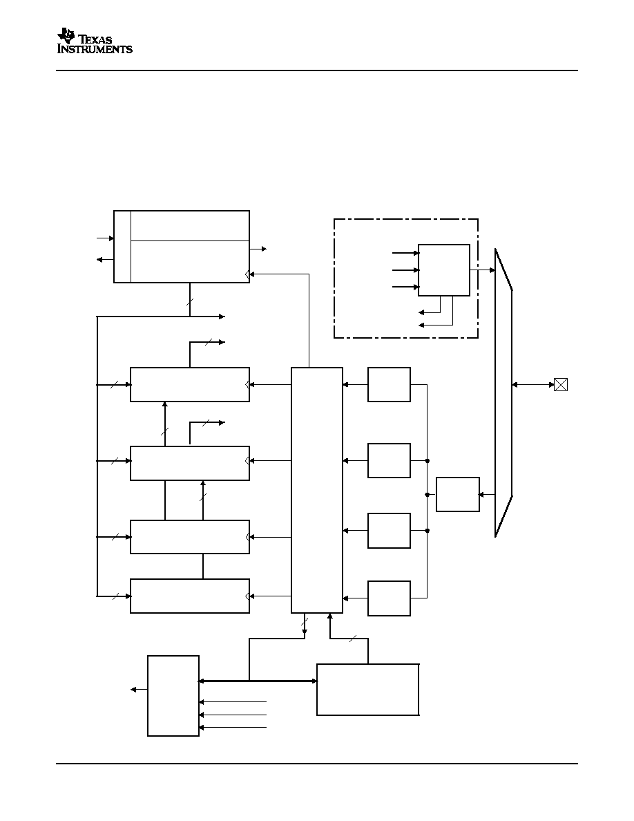
www.ti.com
4.4
Enhanced CAP Modules (eCAP1/2/3/4)
TSCTR
(counter-32 bit)
RST
CAP1
(APRD active)
LD
CAP2
(ACMP active)
LD
CAP3
(APRD shadow)
LD
CAP4
(ACMP shadow)
LD
Continuous /
Oneshot
Capture Control
LD1
LD2
LD3
LD4
32
32
PRD [0-31]
CMP [0-31]
CTR [0-31]
eCAPx
Interrupt
Trigger
and
Flag
control
to PIE
CTR=CMP
32
32
32
32
32
ACMP
shadow
Event
Pre-scale
CTRPHS
(phase register-32 bit)
SYNCOut
SYNCIn
Event
qualifier
Polarity
select
Polarity
select
Polarity
select
Polarity
select
CTR=PRD
CTR_OVF
4
PWM
compare
logic
CTR [0-31]
PRD [0-31]
CMP [0-31]
CTR=CMP
CTR=PRD
CTR_OVF
OVF
APWM mode
Delta-mode
SYNC
4
Capture events
CEVT[1:4]
APRD
shadow
32
32
MODE SELECT
TMS320F2809, TMS320F2808, TMS320F2806
TMS320F2802, TMS320F2801, UCD9501
TMS320C2802, TMS320C2801 Digital Signal Processors
SPRS230G ≠ OCTOBER 2003 ≠ REVISED FEBRUARY 2006
The 280x device contains up to four enhanced capture (eCAP) modules.
Figure 4-5
shows a functional
block diagram of a module. See the TMS320x280x Enhanced Capture (eCAP) Module Reference Guide
(literature number SPRU807) for more details.
The eCAP modules are clocked at the SYSCLKOUT rate.
The clock enable bits (ECAP1/2/3/4ENCLK) in the PCLKCR1 register are used to turn off the eCAP
modules
individually
(for
low
power
operation).
Upon
reset,
ECAP1ENCLK,
ECAP2ENCLK,
ECAP3ENCLK, and ECAP4ENCLK are set to low, indicating that the peripheral clock is off.
Figure 4-5. eCAP Functional Block Diagram
Peripherals
57

www.ti.com
TMS320F2809, TMS320F2808, TMS320F2806
TMS320F2802, TMS320F2801, UCD9501
TMS320C2802, TMS320C2801 Digital Signal Processors
SPRS230G ≠ OCTOBER 2003 ≠ REVISED FEBRUARY 2006
Table 4-3. eCAP Control and Status Registers
SIZE
NAME
ECAP1
ECAP2
ECAP3
ECAP4
DESCRIPTION
(x16)
TSCTR
0x6A00
0x6A20
0x6A40
0x6A60
2
Time-Stamp Counter
CTRPHS
0x6A02
0x6A22
0x6A42
0x6A62
2
Counter Phase Offset Value Register
CAP1
0x6A04
0x6A24
0x6A44
0x6A64
2
Capture 1 Register
CAP2
0x6A06
0x6A26
0x6A46
0x6A66
2
Capture 2 Register
CAP3
0x6A08
0x6A28
0x6A48
0x6A68
2
Capture 3 Register
CAP4
0x6A0A
0x6A2A
0x6A4A
0x6A6A
2
Capture 4 Register
Reserved
0x6A0C-
0x6A2C-
0x6A4C-
0x6A6C-
8
0x6A12
0x6A32
0x6A52
0x6A72
ECCTL1
0x6A14
0x6A34
0x6A54
0x6A74
1
Capture Control Register 1
ECCTL2
0x6A15
0x6A35
0x6A55
0x6A75
1
Capture Control Register 2
ECEINT
0x6A16
0x6A36
0x6A56
0x6A76
1
Capture Interrupt Enable Register
ECFLG
0x6A17
0x6A37
0x6A57
0x6A77
1
Capture Interrupt Flag Register
ECCLR
0x6A18
0x6A38
0x6A58
0x6A78
1
Capture Interrupt Clear Register
ECFRC
0x6A19
0x6A39
0x6A59
0x6A79
1
Capture Interrupt Force Register
Reserved
0x6A1A-
0x6A3A-
0x6A5A-
0x6A7A-
6
0x6A1F
0x6A3F
0x6A5F
0x6A7F
Peripherals
58
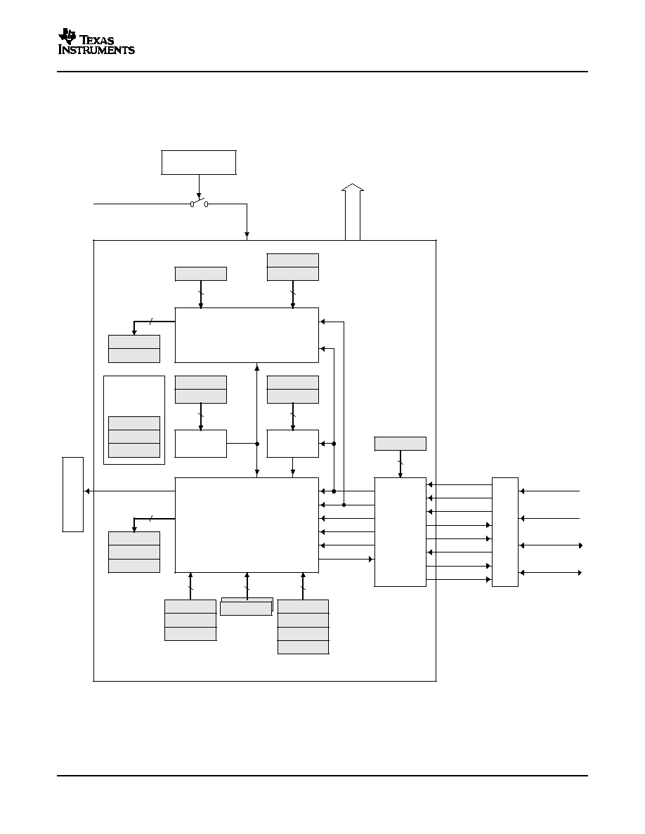
www.ti.com
4.5
Enhanced QEP Modules (eQEP1/2)
QWDTMR
QWDPRD
16
QWDOG
UTIME
QUPRD
QUTMR
32
UTOUT
WDTOUT
Quadrature
capture unit
(QCAP)
QCPRDLAT
QCTMRLAT
16
QFLG
QEPSTS
QEPCTL
Registers
used by
multiple units
QCLK
QDIR
QI
QS
PHE
PCSOUT
Quadrature
decoder
(QDU)
QDECCTL
16
Position counter/
control unit
(PCCU)
QPOSLAT
QPOSSLAT
16
QPOSILAT
EQEPxAIN
EQEPxBIN
EQEPxIIN
EQEPxIOUT
EQEPxIOE
EQEPxSIN
EQEPxSOUT
EQEPxSOE
GPIO
MUX
EQEPxA/XCLK
EQEPxB/XDIR
EQEPxS
EQEPxI
QPOSCMP
QEINT
QFRC
32
QCLR
QPOSCTL
16
32
QPOSCNT
QPOSMAX
QPOSINIT
PIE
EQEPxINT
Enhanced QEP (eQEP) peripheral
System
control registers
QCTMR
QCPRD
16
16
QCAPCTL
EQEPxENCLK
SYSCLKOUT
Data bus
To CPU
TMS320F2809, TMS320F2808, TMS320F2806
TMS320F2802, TMS320F2801, UCD9501
TMS320C2802, TMS320C2801 Digital Signal Processors
SPRS230G ≠ OCTOBER 2003 ≠ REVISED FEBRUARY 2006
The 280x device contains up to two enhanced quadrature encoder (eQEP) modules. See the
TMS320x280x Enhanced Quadrature Encoder (eQEP) Module Reference Guide (literature number
SPRU790) for more details.
Figure 4-6. eQEP Functional Block Diagram
Peripherals
59

www.ti.com
TMS320F2809, TMS320F2808, TMS320F2806
TMS320F2802, TMS320F2801, UCD9501
TMS320C2802, TMS320C2801 Digital Signal Processors
SPRS230G ≠ OCTOBER 2003 ≠ REVISED FEBRUARY 2006
Table 4-4. eQEP Control and Status Registers
EQEP1
EQEP1
EQEP2
NAME
SIZE(x16)/
REGISTER DESCRIPTION
ADDRESS
ADDRESS
#SHADOW
QPOSCNT
0x6B00
0x6B40
2/0
eQEP Position Counter
QPOSINIT
0x6B02
0x6B42
2/0
eQEP Initialization Position Count
QPOSMAX
0x6B04
0x6B44
2/0
eQEP Maximum Position Count
QPOSCMP
0x6B06
0x6B46
2/1
eQEP Position-compare
QPOSILAT
0x6B08
0x6B48
2/0
eQEP Index Position Latch
QPOSSLAT
0x6B0A
0x6B4A
2/0
eQEP Strobe Position Latch
QPOSLAT
0x6B0C
0x6B4C
2/0
eQEP Position Latch
QUTMR
0x6B0E
0x6B4E
2/0
eQEP Unit Timer
QUPRD
0x6B10
0x6B50
2/0
eQEP Unit Period Register
QWDTMR
0x6B12
0x6B52
1/0
eQEP Watchdog Timer
QWDPRD
0x6B13
0x6B53
1/0
eQEP Watchdog Period Register
QDECCTL
0x6B14
0x6B54
1/0
eQEP Decoder Control Register
QEPCTL
0x6B15
0x6B55
1/0
eQEP Control Register
QCAPCTL
0x6B16
0x6B56
1/0
eQEP Capture Control Register
QPOSCTL
0x6B17
0x6B57
1/0
eQEP Position-compare Control Register
QEINT
0x6B18
0x6B58
1/0
eQEP Interrupt Enable Register
QFLG
0x6B19
0x6B59
1/0
eQEP Interrupt Flag Register
QCLR
0x6B1A
0x6B5A
1/0
eQEP Interrupt Clear Register
QFRC
0x6B1B
0x6B5B
1/0
eQEP Interrupt Force Register
QEPSTS
0x6B1C
0x6B5C
1/0
eQEP Status Register
QCTMR
0x6B1D
0x6B5D
1/0
eQEP Capture Timer
QCPRD
0x6B1E
0x6B5E
1/0
eQEP Capture Period Register
QCTMRLAT
0x6B1F
0x6B5F
1/0
eQEP Capture Timer Latch
QCPRDLAT
0x6B20
0x6B60
1/0
eQEP Capture Period Latch
Reserved
0x6B21-
0x6B61-
31/0
0x6B3F
0x6B7F
Peripherals
60

www.ti.com
4.6
Enhanced Analog-to-Digital Converter (ADC) Module
Digital Value
+
0,
Digital Value
+
4096
Input Analog Voltage
*
ADCLO
3
when input
0 V
when 0 V < input < 3 V
when input
3 V
Digital Value
+
4095,
TMS320F2809, TMS320F2808, TMS320F2806
TMS320F2802, TMS320F2801, UCD9501
TMS320C2802, TMS320C2801 Digital Signal Processors
SPRS230G ≠ OCTOBER 2003 ≠ REVISED FEBRUARY 2006
A simplified functional block diagram of the ADC module is shown in
Figure 4-7
. The ADC module
consists of a 12-bit ADC with a built-in sample-and-hold (S/H) circuit. Functions of the ADC module
include:
∑
12-bit ADC core with built-in S/H
∑
Analog input: 0.0 V to 3.0 V (Voltages above 3.0 V produce full-scale conversion results.)
∑
Fast conversion rate: 160 ns at 12.5-MHz ADC clock, 6.25 MSPS
∑
16-channel, MUXed inputs
∑
Autosequencing capability provides up to 16 "autoconversions" in a single session. Each conversion
can be programmed to select any 1 of 16 input channels
∑
Sequencer can be operated as two independent 8-state sequencers or as one large 16-state
sequencer (i.e., two cascaded 8-state sequencers)
∑
Sixteen result registers (individually addressable) to store conversion values
≠
The digital value of the input analog voltage is derived by:
A.
All fractional values are truncated.
∑
Multiple triggers as sources for the start-of-conversion (SOC) sequence
≠
S/W - software immediate start
≠
ePWM start of conversion
≠
XINT2 ADC start of conversion
∑
Flexible interrupt control allows interrupt request on every end-of-sequence (EOS) or every other EOS.
∑
Sequencer can operate in "start/stop" mode, allowing multiple "time-sequenced triggers" to
synchronize conversions.
∑
SOCA and SOCB triggers can operate independently in dual-sequencer mode.
∑
Sample-and-hold (S/H) acquisition time window has separate prescale control.
The ADC module in the 280x has been enhanced to provide flexible interface to ePWM peripherals. The
ADC interface is built around a fast, 12-bit ADC module with a fast conversion rate of 160 ns at 12.5-MHz
ADC clock. The ADC module has 16 channels, configurable as two independent 8-channel modules. The
two independent 8-channel modules can be cascaded to form a 16-channel module. Although there are
multiple input channels and two sequencers, there is only one converter in the ADC module.
Figure 4-7
shows the block diagram of the ADC module.
The two 8-channel modules have the capability to autosequence a series of conversions, each module
has the choice of selecting any one of the respective eight channels available through an analog MUX. In
the cascaded mode, the autosequencer functions as a single 16-channel sequencer. On each sequencer,
once the conversion is complete, the selected channel value is stored in its respective RESULT register.
Autosequencing allows the system to convert the same channel multiple times, allowing the user to
perform oversampling algorithms. This gives increased resolution over traditional single-sampled
conversion results.
Peripherals
61
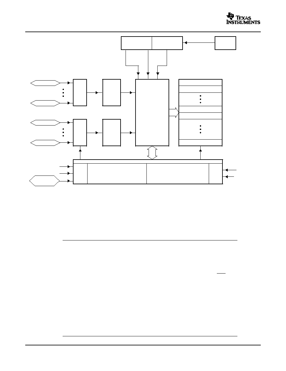
www.ti.com
Result Registers
EPWMSOCB
S/W
GPIO/XINT2
_ADCSOC
EPWMSOCA
S/W
Sequencer 2
Sequencer 1
SOC
SOC
ADC Control Registers
70B7h
70B0h
70AFh
70A8h
Result Reg 15
Result Reg 8
Result Reg 7
Result Reg 1
Result Reg 0
Module
ADC
12-Bit
Analog
MUX
ADCINA0
ADCINA7
ADCINB0
ADCINB7
System
Control Block
High-Speed
Prescaler
HSPCLK
ADCENCLK
DSP
SYSCLKOUT
S/H
S/H
HALT
TMS320F2809, TMS320F2808, TMS320F2806
TMS320F2802, TMS320F2801, UCD9501
TMS320C2802, TMS320C2801 Digital Signal Processors
SPRS230G ≠ OCTOBER 2003 ≠ REVISED FEBRUARY 2006
Figure 4-7. Block Diagram of the ADC Module
To obtain the specified accuracy of the ADC, proper board layout is very critical. To the best extent
possible, traces leading to the ADCIN pins should not run in close proximity to the digital signal paths.
This is to minimize switching noise on the digital lines from getting coupled to the ADC inputs.
Furthermore, proper isolation techniques must be used to isolate the ADC module power pins ( V
DD1A18
,
V
DD2A18
, V
DDA2
, V
DDAIO
) from the digital supply.
Figure 4-8
shows the ADC pin connections for the 280x
devices.
NOTE
1. The ADC registers are accessed at the SYSCLKOUT rate. The internal timing of the
ADC module is controlled by the high-speed peripheral clock (HSPCLK).
2. The behavior of the ADC module based on the state of the ADCENCLK and HALT
signals is as follows:
≠
ADCENCLK: On reset, this signal will be low. While reset is active-low (XRS) the
clock to the register will still function. This is necessary to make sure all registers
and modes go into their default reset state. The analog module, however, will be
in a low-power inactive state. As soon as reset goes high, then the clock to the
registers will be disabled. When the user sets the ADCENCLK signal high, then
the clocks to the registers will be enabled and the analog module will be enabled.
There will be a certain time delay (ms range) before the ADC is stable and can be
used.
≠
HALT: This mode only affects the analog module. It does not affect the registers.
In this mode, the ADC module goes into low-power mode. This mode also will stop
the clock to the CPU, which will stop the HSPCLK; therefore, the ADC register
logic will be turned off indirectly.
62
Peripherals

www.ti.com
ADCINA[7:0]
ADCINB[7:0]
ADCLO
ADCREFIN
ADC External Current Bias Resistor
ADCRESEXT
ADCREFP
V
DD1A18
V
DD2A18
V
SS1AGND
V
SS2AGND
V
DDAIO
V
SSAIO
V
DDA2
V
SSA2
ADC Reference Positive Output
ADCREFM
ADC Reference Medium Output
ADC Power
ADC Analog and Reference I/O Power
Analog input 0-3 V with respect to ADCLO
Connect to analog ground
22 k
W
2.2
m
F
(A)
2.2
m
F
(A)
ADC Analog Power Pin (1.8 V)
ADC Analog Power Pin (1.8 V)
ADC Analog Power Pin (3.3 V)
ADC Analog I/O Ground Pin
ADC Analog Power Pin (3.3 V)
ADCREFP and ADCREFM should not
be loaded by external circuitry
ADC Analog Ground Pin
ADC 16-Channel Analog Inputs
Float or ground if internal reference is used
ADC Analog Ground Pin
ADC Analog Ground Pin
TMS320F2809, TMS320F2808, TMS320F2806
TMS320F2802, TMS320F2801, UCD9501
TMS320C2802, TMS320C2801 Digital Signal Processors
SPRS230G ≠ OCTOBER 2003 ≠ REVISED FEBRUARY 2006
Figure 4-8
shows the ADC pin-biasing for internal reference and
Figure 4-9
shows the ADC pin-biasing for
external reference.
A.
TAIYO YUDEN LMK212BJ225MG-T or equivalent
B.
External decoupling capacitors are recommended on all power pins.
C.
Analog inputs must be driven from an operational amplifier that does not degrade the ADC performance.
Figure 4-8. ADC Pin Connections With Internal Reference
Peripherals
63

www.ti.com
ADCINA[7:0]
ADCINB[7:0]
ADCLO
ADCREFIN
ADC External Current Bias Resistor
ADCRESEXT
ADCREFP
V
DD1A18
V
DD2A18
V
SS1AGND
V
SS2AGND
V
DDAIO
V
SSAIO
V
DDA2
V
SSA2
ADC Reference Positive Output
ADCREFM
ADC Reference Medium Output
ADC Analog Power
ADC Analog and Reference I/O Power
Analog input 0-3 V with respect to ADCLO
Connect to Analog Ground
22 k
W
2.2
m
F
(A)
2.2
m
F
(A)
ADCREFP and ADCREFM should not
be loaded by external circuitry
ADC 16-Channel Analog Inputs
Connect to 1.500, 1.024, or 2.048-V precision source
(D)
ADC Analog Power Pin (1.8 V)
ADC Analog Power Pin (1.8 V)
ADC Analog I/O Ground Pin
ADC Analog Power Pin (3.3 V)
ADC Analog Ground Pin
ADC Analog Ground Pin
ADC Analog Ground Pin
ADC Analog Power Pin (3.3 V)
TMS320F2809, TMS320F2808, TMS320F2806
TMS320F2802, TMS320F2801, UCD9501
TMS320C2802, TMS320C2801 Digital Signal Processors
SPRS230G ≠ OCTOBER 2003 ≠ REVISED FEBRUARY 2006
A.
TAIYO YUDEN LMK212BJ225MG-T or equivalent
B.
External decoupling capacitors are recommended on all power pins.
C.
Analog inputs must be driven from an operational amplifier that does not degrade the ADC performance.
D.
External voltage on ADCREFIN is enabled by changing bits 15:14 in the ADC Reference Select register depending on
the voltage used on this pin. TI recommends TI part REF3020 or equivalent for 2.048-V generation. Overall gain
accuracy will be determined by accuracy of this voltage source.
Figure 4-9. ADC Pin Connections With External Reference
NOTE
The temperature rating of any recommended component must match the rating of the end
product.
The ADC operation is configured, controlled, and monitored by the registers listed in
Table 4-5
.
Peripherals
64
www.ti.com
TMS320F2809, TMS320F2808, TMS320F2806
TMS320F2802, TMS320F2801, UCD9501
TMS320C2802, TMS320C2801 Digital Signal Processors
SPRS230G ≠ OCTOBER 2003 ≠ REVISED FEBRUARY 2006
Table 4-5. ADC Registers
(1)
NAME
ADDRESS
(1)
ADDRESS
(2)
SIZE (x16)
DESCRIPTION
ADCTRL1
0x7100
1
ADC Control Register 1
ADCTRL2
0x7101
1
ADC Control Register 2
ADCMAXCONV
0x7102
1
ADC Maximum Conversion Channels Register
ADCCHSELSEQ1
0x7103
1
ADC Channel Select Sequencing Control Register 1
ADCCHSELSEQ2
0x7104
1
ADC Channel Select Sequencing Control Register 2
ADCCHSELSEQ3
0x7105
1
ADC Channel Select Sequencing Control Register 3
ADCCHSELSEQ4
0x7106
1
ADC Channel Select Sequencing Control Register 4
ADCASEQSR
0x7107
1
ADC Auto-Sequence Status Register
ADCRESULT0
0x7108
0x0B00
1
ADC Conversion Result Buffer Register 0
ADCRESULT1
0x7109
0x0B01
1
ADC Conversion Result Buffer Register 1
ADCRESULT2
0x710A
0x0B02
1
ADC Conversion Result Buffer Register 2
ADCRESULT3
0x710B
0x0B03
1
ADC Conversion Result Buffer Register 3
ADCRESULT4
0x710C
0x0B04
1
ADC Conversion Result Buffer Register 4
ADCRESULT5
0x710D
0x0B05
1
ADC Conversion Result Buffer Register 5
ADCRESULT6
0x710E
0x0B06
1
ADC Conversion Result Buffer Register 6
ADCRESULT7
0x710F
0x0B07
1
ADC Conversion Result Buffer Register 7
ADCRESULT8
0x7110
0x0B08
1
ADC Conversion Result Buffer Register 8
ADCRESULT9
0x7111
0x0B09
1
ADC Conversion Result Buffer Register 9
ADCRESULT10
0x7112
0x0B0A
1
ADC Conversion Result Buffer Register 10
ADCRESULT11
0x7113
0x0B0B
1
ADC Conversion Result Buffer Register 11
ADCRESULT12
0x7114
0x0B0C
1
ADC Conversion Result Buffer Register 12
ADCRESULT13
0x7115
0x0B0D
1
ADC Conversion Result Buffer Register 13
ADCRESULT14
0x7116
0x0B0E
1
ADC Conversion Result Buffer Register 14
ADCRESULT15
0x7117
0x0B0F
1
ADC Conversion Result Buffer Register 15
ADCTRL3
0x7118
1
ADC Control Register 3
ADCST
0x7119
1
ADC Status Register
0x711A
Reserved
2
0x711B
ADCREFSEL
0x711C
1
ADC Reference Select Register
ADCOFFTRIM
0x711D
1
ADC Offset Trim Register
0x711E
Reserved
2
ADC Status Register
0x711F
(1)
The registers in this column are Peripheral Frame 2 Registers.
(2)
The ADC result registers are dual mapped in the 280x DSP. Locations in Peripheral Frame 2 (0x7108-0x7117) are 2 wait states and left
justified. Locations in Peripheral frame 0 space (0x0B00-0x0B0F) are 0 wait sates and right justified. During high speed/continuous
conversion use of the ADC, use the 0 wait state locations for fast transfer of ADC results to user memory.
Peripherals
65

www.ti.com
4.7
Enhanced Controller Area Network (eCAN) Modules (eCAN-A and eCAN-B)
TMS320F2809, TMS320F2808, TMS320F2806
TMS320F2802, TMS320F2801, UCD9501
TMS320C2802, TMS320C2801 Digital Signal Processors
SPRS230G ≠ OCTOBER 2003 ≠ REVISED FEBRUARY 2006
The CAN module has the following features:
∑
Fully compliant with CAN protocol, version 2.0B
∑
Supports data rates up to 1 Mbps
∑
Thirty-two mailboxes, each with the following properties:
≠
Configurable as receive or transmit
≠
Configurable with standard or extended identifier
≠
Has a programmable receive mask
≠
Supports data and remote frame
≠
Composed of 0 to 8 bytes of data
≠
Uses a 32-bit time stamp on receive and transmit message
≠
Protects against reception of new message
≠
Holds the dynamically programmable priority of transmit message
≠
Employs a programmable interrupt scheme with two interrupt levels
≠
Employs a programmable alarm on transmission or reception time-out
∑
Low-power mode
∑
Programmable wake-up on bus activity
∑
Automatic reply to a remote request message
∑
Automatic retransmission of a frame in case of loss of arbitration or error
∑
32-bit local network time counter synchronized by a specific message (communication in conjunction
with mailbox 16)
∑
Self-test mode
≠
Operates in a loopback mode receiving its own message. A "dummy" acknowledge is provided,
thereby eliminating the need for another node to provide the acknowledge bit.
NOTE
For a SYSCLKOUT of 100 MHz, the smallest bit rate possible is 15.6 kbps.
66
Peripherals
www.ti.com
Mailbox RAM
(512 Bytes)
32-Message Mailbox
of 4
◊
32-Bit Words
Memory Management
Unit
CPU Interface,
Receive Control Unit,
Timer Management Unit
eCAN Memory
(512 Bytes)
Registers and Message
Objects Control
32
32
Message Controller
32
32
32
32
32
32
eCAN Protocol Kernel
Receive Buffer
Transmit Buffer
Control Buffer
Status Buffer
Enhanced CAN Controller
32
Controls
Address
Data
eCAN1INT
eCAN0INT
32
SN65HVD23x
3.3-V CAN Transceiver
CAN Bus
TMS320F2809, TMS320F2808, TMS320F2806
TMS320F2802, TMS320F2801, UCD9501
TMS320C2802, TMS320C2801 Digital Signal Processors
SPRS230G ≠ OCTOBER 2003 ≠ REVISED FEBRUARY 2006
Figure 4-10. eCAN Block Diagram and Interface Circuit
Table 4-6. 3.3-V eCAN Transceivers
SUPPLY
LOW-POWER
SLOPE
PART NUMBER
VREF
OTHER
T
A
VOLTAGE
MODE
CONTROL
SN65HVD230
3.3 V
Standby
Adjustable
Yes
≠
-40
∞
C to 85
∞
C
SN65HVD230Q
3.3 V
Standby
Adjustable
Yes
≠
-40
∞
C to 125
∞
C
SN65HVD231
3.3 V
Sleep
Adjustable
Yes
≠
-40
∞
C to 85
∞
C
SN65HVD231Q
3.3 V
Sleep
Adjustable
Yes
≠
-40
∞
C to 125
∞
C
SN65HVD232
3.3 V
None
None
None
≠
-40
∞
C to 85
∞
C
SN65HVD232Q
3.3 V
None
None
None
≠
-40
∞
C to 125
∞
C
SN65HVD233
3.3 V
Standby
Adjustable
None
Diagnostic
-40
∞
C to 125
∞
C
Loopback
SN65HVD234
3.3 V
Standby & Sleep
Adjustable
None
≠
-40
∞
C to 125
∞
C
SN65HVD235
3.3 V
Standby
Adjustable
None
Autobaud
-40
∞
C to 125
∞
C
Loopback
Peripherals
67
www.ti.com
Mailbox Enable - CANME
Mailbox Direction - CANMD
Transmission Request Set - CANTRS
Transmission Request Reset - CANTRR
Transmission Acknowledge - CANTA
Abort Acknowledge - CANAA
Received Message Pending - CANRMP
Received Message Lost - CANRML
Remote Frame Pending - CANRFP
Global Acceptance Mask - CANGAM
Master Control - CANMC
Bit-Timing Configuration - CANBTC
Error and Status - CANES
Transmit Error Counter - CANTEC
Receive Error Counter - CANREC
Global Interrupt Flag 0 - CANGIF0
Global Interrupt Mask - CANGIM
Mailbox Interrupt Mask - CANMIM
Mailbox Interrupt Level - CANMIL
Overwrite Protection Control - CANOPC
TX I/O Control - CANTIOC
RX I/O Control - CANRIOC
Time Stamp Counter - CANTSC
Global Interrupt Flag 1 - CANGIF1
Time-Out Control - CANTOC
Time-Out Status - CANTOS
Reserved
eCAN-A Control and Status Registers
Message Identifier - MSGID
61E8h-61E9h
Message Control - MSGCTRL
Message Data Low - MDL
Message Data High - MDH
Message Mailbox (16 Bytes)
Control and Status Registers
6000h
603Fh
Local Acceptance Masks (LAM)
(32
◊
32-Bit RAM)
6040h
607Fh
6080h
60BFh
60C0h
60FFh
eCAN-A Memory (512 Bytes)
Message Object Time Stamps (MOTS)
(32
◊
32-Bit RAM)
Message Object Time-Out (MOTO)
(32
◊
32-Bit RAM)
Mailbox 0
6100h-6107h
Mailbox 1
6108h-610Fh
Mailbox 2
6110h-6117h
Mailbox 3
6118h-611Fh
eCAN-A Memory RAM (512 Bytes)
Mailbox 4
6120h-6127h
Mailbox 28
61E0h-61E7h
Mailbox 29
61E8h-61EFh
Mailbox 30
61F0h-61F7h
Mailbox 31
61F8h-61FFh
61EAh-61EBh
61ECh-61EDh
61EEh-61EFh
TMS320F2809, TMS320F2808, TMS320F2806
TMS320F2802, TMS320F2801, UCD9501
TMS320C2802, TMS320C2801 Digital Signal Processors
SPRS230G ≠ OCTOBER 2003 ≠ REVISED FEBRUARY 2006
Figure 4-11. eCAN-A Memory Map
68
Peripherals
www.ti.com
Mailbox Enable - CANME
Mailbox Direction - CANMD
Transmission Request Set - CANTRS
Transmission Request Reset - CANTRR
Transmission Acknowledge - CANTA
Abort Acknowledge - CANAA
Received Message Pending - CANRMP
Received Message Lost - CANRML
Remote Frame Pending - CANRFP
Global Acceptance Mask - CANGAM
Master Control - CANMC
Bit-Timing Configuration - CANBTC
Error and Status - CANES
Transmit Error Counter - CANTEC
Receive Error Counter - CANREC
Global Interrupt Flag 0 - CANGIF0
Global Interrupt Mask - CANGIM
Mailbox Interrupt Mask - CANMIM
Mailbox Interrupt Level - CANMIL
Overwrite Protection Control - CANOPC
TX I/O Control - CANTIOC
RX I/O Control - CANRIOC
Time Stamp Counter - CANTSC
Global Interrupt Flag 1 - CANGIF1
Time-Out Control - CANTOC
Time-Out Status - CANTOS
Reserved
eCAN-B Control and Status Registers
Message Identifier - MSGID
63E8h-63E9h
Message Control - MSGCTRL
Message Data Low - MDL
Message Data High - MDH
Message Mailbox (16 Bytes)
Control and Status Registers
6200h
623Fh
Local Acceptance Masks (LAM)
(32
◊
32-Bit RAM)
6240h
627Fh
6280h
62BFh
62C0h
62FFh
eCAN-B Memory (512 Bytes)
Message Object Time Stamps (MOTS)
(32
◊
32-Bit RAM)
Message Object Time-Out (MOTO)
(32
◊
32-Bit RAM)
Mailbox 0
6300h-6307h
Mailbox 1
6308h-630Fh
Mailbox 2
6310h-6317h
Mailbox 3
6318h-631Fh
eCAN-B Memory RAM (512 Bytes)
Mailbox 4
6320h-6327h
Mailbox 28
63E0h-63E7h
Mailbox 29
63E8h-63EFh
Mailbox 30
63F0h-63F7h
Mailbox 31
63F8h-63FFh
63EAh-63EBh
63ECh-63EDh
63EEh-63EFh
TMS320F2809, TMS320F2808, TMS320F2806
TMS320F2802, TMS320F2801, UCD9501
TMS320C2802, TMS320C2801 Digital Signal Processors
SPRS230G ≠ OCTOBER 2003 ≠ REVISED FEBRUARY 2006
Figure 4-12. eCAN-B Memory Map
The CAN registers listed in
Table 4-7
are used by the CPU to configure and control the CAN controller
and the message objects. eCAN control registers only support 32-bit read/write operations. Mailbox RAM
can be accessed as 16 bits or 32 bits. 32-bit accesses are aligned to an even boundary.
Peripherals
69
www.ti.com
TMS320F2809, TMS320F2808, TMS320F2806
TMS320F2802, TMS320F2801, UCD9501
TMS320C2802, TMS320C2801 Digital Signal Processors
SPRS230G ≠ OCTOBER 2003 ≠ REVISED FEBRUARY 2006
Table 4-7. CAN Register Map
(1)
ECAN-A
ECAN-B
SIZE
REGISTER NAME
DESCRIPTION
ADDRESS
ADDRESS
(x32)
CANME
0x6000
0x6200
1
Mailbox enable
CANMD
0x6002
0x6202
1
Mailbox direction
CANTRS
0x6004
0x6204
1
Transmit request set
CANTRR
0x6006
0x6206
1
Transmit request reset
CANTA
0x6008
0x6208
1
Transmission acknowledge
CANAA
0x600A
0x620A
1
Abort acknowledge
CANRMP
0x600C
0x620C
1
Receive message pending
CANRML
0x600E
0x620E
1
Receive message lost
CANRFP
0x6010
0x6210
1
Remote frame pending
CANGAM
0x6012
0x6212
1
Global acceptance mask
CANMC
0x6014
0x6214
1
Master control
CANBTC
0x6016
0x6216
1
Bit-timing configuration
CANES
0x6018
0x6218
1
Error and status
CANTEC
0x601A
0x621A
1
Transmit error counter
CANREC
0x601C
0x621C
1
Receive error counter
CANGIF0
0x601E
0x621E
1
Global interrupt flag 0
CANGIM
0x6020
0x6220
1
Global interrupt mask
CANGIF1
0x6022
0x6222
1
Global interrupt flag 1
CANMIM
0x6024
0x6224
1
Mailbox interrupt mask
CANMIL
0x6026
0x6226
1
Mailbox interrupt level
CANOPC
0x6028
0x6228
1
Overwrite protection control
CANTIOC
0x602A
0x622A
1
TX I/O control
CANRIOC
0x602C
0x622C
1
RX I/O control
CANTSC
0x602E
0x622E
1
Time stamp counter (Reserved in SCC mode)
CANTOC
0x6030
0x6230
1
Time-out control (Reserved in SCC mode)
CANTOS
0x6032
0x6232
1
Time-out status (Reserved in SCC mode)
(1)
These registers are mapped to Peripheral Frame 1.
Peripherals
70

www.ti.com
4.8
Serial Communications Interface (SCI) Modules (SCI-A, SCI-B)
Baud rate =
LSPCLK
16
LSPCLK
(BRR
)
1) * 8
when BRR
0
Baud rate =
when BRR = 0
∑
Max bit rate
+
100 MHz
16
+
6.25
10
6
b s
TMS320F2809, TMS320F2808, TMS320F2806
TMS320F2802, TMS320F2801, UCD9501
TMS320C2802, TMS320C2801 Digital Signal Processors
SPRS230G ≠ OCTOBER 2003 ≠ REVISED FEBRUARY 2006
The 280x devices include two serial communications interface (SCI) modules. The SCI modules support
digital communications between the CPU and other asynchronous peripherals that use the standard
non-return-to-zero (NRZ) format. The SCI receiver and transmitter are double-buffered, and each has its
own separate enable and interrupt bits. Both can be operated independently or simultaneously in the
full-duplex mode. To ensure data integrity, the SCI checks received data for break detection, parity,
overrun, and framing errors. The bit rate is programmable to over 65000 different speeds through a 16-bit
baud-select register.
Features of each SCI module include:
∑
Two external pins:
≠
SCITXD: SCI transmit-output pin
≠
SCIRXD: SCI receive-input pin
NOTE: Both pins can be used as GPIO if not used for SCI.
≠
Baud rate programmable to 64K different rates:
∑
Data-word format
≠
One start bit
≠
Data-word length programmable from one to eight bits
≠
Optional even/odd/no parity bit
≠
One or two stop bits
∑
Four error-detection flags: parity, overrun, framing, and break detection
∑
Two wake-up multiprocessor modes: idle-line and address bit
∑
Half- or full-duplex operation
∑
Double-buffered receive and transmit functions
∑
Transmitter and receiver operations can be accomplished through interrupt-driven or polled algorithms
with status flags.
≠
Transmitter: TXRDY flag (transmitter-buffer register is ready to receive another character) and TX
EMPTY flag (transmitter-shift register is empty)
≠
Receiver: RXRDY flag (receiver-buffer register is ready to receive another character), BRKDT flag
(break condition occurred), and RX ERROR flag (monitoring four interrupt conditions)
∑
Separate enable bits for transmitter and receiver interrupts (except BRKDT)
∑
NRZ (non-return-to-zero) format
∑
Ten SCI module control registers located in the control register frame beginning at address 7050h
NOTE
All registers in this module are 8-bit registers that are connected to Peripheral Frame 2.
When a register is accessed, the register data is in the lower byte (7-0), and the upper
byte (15-8) is read as zeros. Writing to the upper byte has no effect.
Enhanced features:
∑
Auto baud-detect hardware logic
∑
16-level transmit/receive FIFO
The SCI port operation is configured and controlled by the registers listed in
Table 4-8
and
Table 4-9
.
Peripherals
71
www.ti.com
TMS320F2809, TMS320F2808, TMS320F2806
TMS320F2802, TMS320F2801, UCD9501
TMS320C2802, TMS320C2801 Digital Signal Processors
SPRS230G ≠ OCTOBER 2003 ≠ REVISED FEBRUARY 2006
Table 4-8. SCI-A Registers
(1)
NAME
ADDRESS
SIZE (x16)
DESCRIPTION
SCICCRA
0x7050
1
SCI-A Communications Control Register
SCICTL1A
0x7051
1
SCI-A Control Register 1
SCIHBAUDA
0x7052
1
SCI-A Baud Register, High Bits
SCILBAUDA
0x7053
1
SCI-A Baud Register, Low Bits
SCICTL2A
0x7054
1
SCI-A Control Register 2
SCIRXSTA
0x7055
1
SCI-A Receive Status Register
SCIRXEMUA
0x7056
1
SCI-A Receive Emulation Data Buffer Register
SCIRXBUFA
0x7057
1
SCI-A Receive Data Buffer Register
SCITXBUFA
0x7059
1
SCI-A Transmit Data Buffer Register
SCIFFTXA
(2)
0x705A
1
SCI-A FIFO Transmit Register
SCIFFRXA
(2)
0x705B
1
SCI-A FIFO Receive Register
SCIFFCTA
(2)
0x705C
1
SCI-A FIFO Control Register
SCIPRIA
0x705F
1
SCI-A Priority Control Register
(1)
Registers in this table are mapped to Peripheral Frame 2 space. This space only allows 16-bit accesses. 32-bit accesses produce
undefined results.
(2)
These registers are new registers for the FIFO mode.
Table 4-9. SCI-B Registers
(1) (2)
NAME
ADDRESS
SIZE (x16)
DESCRIPTION
SCICCRB
0x7750
1
SCI-B Communications Control Register
SCICTL1B
0x7751
1
SCI-B Control Register 1
SCIHBAUDB
0x7752
1
SCI-B Baud Register, High Bits
SCILBAUDB
0x7753
1
SCI-B Baud Register, Low Bits
SCICTL2B
0x7754
1
SCI-B Control Register 2
SCIRXSTB
0x7755
1
SCI-B Receive Status Register
SCIRXEMUB
0x7756
1
SCI-B Receive Emulation Data Buffer Register
SCIRXBUFB
0x7757
1
SCI-B Receive Data Buffer Register
SCITXBUFB
0x7759
1
SCI-B Transmit Data Buffer Register
SCIFFTXB
(2)
0x775A
1
SCI-B FIFO Transmit Register
SCIFFRXB
(2)
0x775B
1
SCI-B FIFO Receive Register
SCIFFCTB
(2)
0x775C
1
SCI-B FIFO Control Register
SCIPRIB
0x775F
1
SCI-B Priority Control Register
(1)
Registers in this table are mapped to peripheral bus 16 space. This space only allows 16-bit accesses. 32-bit accesses produce
undefined results.
(2)
These registers are new registers for the FIFO mode.
Peripherals
72
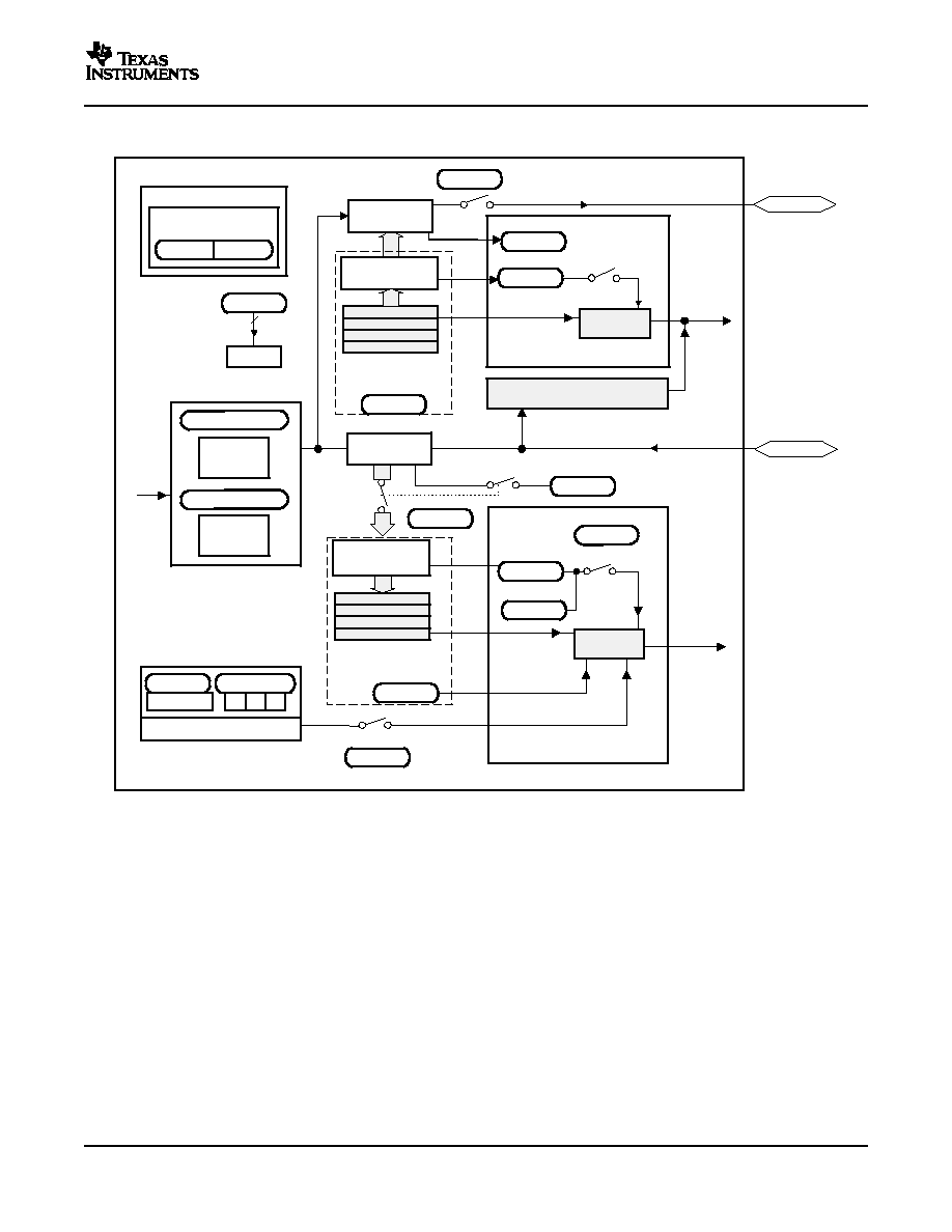
www.ti.com
TX FIFO _0
LSPCLK
WUT
Frame Format and Mode
Even/Odd
Enable
Parity
SCI RX Interrupt select logic
BRKDT
RXRDY
SCIRXST.6
SCICTL1.3
8
SCICTL2.1
RX/BK INT ENA
SCIRXD
SCIRXST.1
TXENA
SCI TX Interrupt select logic
TX EMPTY
TXRDY
SCICTL2.0
TX INT ENA
SCITXD
RXENA
SCIRXD
RXWAKE
SCICTL1.6
RX ERR INT ENA
TXWAKE
SCITXD
SCICCR.6 SCICCR.5
SCITXBUF.7-0
SCIHBAUD. 15 - 8
Baud Rate
MSbyte
Register
SCILBAUD. 7 - 0
Transmitter-Data
Buffer Register
8
SCICTL2.6
SCICTL2.7
Baud Rate
LSbyte
Register
RXSHF
Register
TXSHF
Register
SCIRXST.5
1
TX FIFO _1
-----
TX FIFO _15
8
TX FIFO registers
TX FIFO
TX Interrupt
Logic
TXINT
SCIFFTX.14
RX FIFO _15
SCIRXBUF.7-0
Receive Data
Buffer register
SCIRXBUF.7-0
-----
RX FIFO_1
RX FIFO _0
8
RX FIFO registers
SCICTL1.0
RX Interrupt
Logic
RXINT
RX FIFO
SCIFFRX.15
RXFFOVF
RX Error
SCIRXST.7
PE
FE OE
RX Error
SCIRXST.4 - 2
To CPU
To CPU
AutoBaud Detect logic
SCICTL1.1
SCIFFENA
Interrupts
Interrupts
TMS320F2809, TMS320F2808, TMS320F2806
TMS320F2802, TMS320F2801, UCD9501
TMS320C2802, TMS320C2801 Digital Signal Processors
SPRS230G ≠ OCTOBER 2003 ≠ REVISED FEBRUARY 2006
Figure 4-13
shows the SCI module block diagram.
Figure 4-13. Serial Communications Interface (SCI) Module Block Diagram
Peripherals
73

www.ti.com
4.9
Serial Peripheral Interface (SPI) Modules (SPI-A, SPI-B, SPI-C, SPI-D)
Baud rate =
LSPCLK
4
LSPCLK
(SPIBRR
)
1)
when SPIBRR = 3 to 127
Baud rate =
when SPIBRR = 0,1, 2
TMS320F2809, TMS320F2808, TMS320F2806
TMS320F2802, TMS320F2801, UCD9501
TMS320C2802, TMS320C2801 Digital Signal Processors
SPRS230G ≠ OCTOBER 2003 ≠ REVISED FEBRUARY 2006
The 280x devices include the four-pin serial peripheral interface (SPI) module. Up to four SPI modules
(SPI-A, SPI-B, SPI-C, and SPI-D) are available. The SPI is a high-speed, synchronous serial I/O port that
allows a serial bit stream of programmed length (one to sixteen bits) to be shifted into and out of the
device at a programmable bit-transfer rate. Normally, the SPI is used for communications between the
DSP controller and external peripherals or another processor. Typical applications include external I/O or
peripheral expansion through devices such as shift registers, display drivers, and ADCs. Multidevice
communications are supported by the master/slave operation of the SPI.
The SPI module features include:
∑
Four external pins:
≠
SPISOMI: SPI slave-output/master-input pin
≠
SPISIMO: SPI slave-input/master-output pin
≠
SPISTE: SPI slave transmit-enable pin
≠
SPICLK: SPI serial-clock pin
NOTE: All four pins can be used as GPIO, if the SPI module is not used.
∑
Two operational modes: master and slave
Baud rate: 125 different programmable rates.
∑
Data word length: one to sixteen data bits
∑
Four clocking schemes (controlled by clock polarity and clock phase bits) include:
≠
Falling edge without phase delay: SPICLK active-high. SPI transmits data on the falling edge of the
SPICLK signal and receives data on the rising edge of the SPICLK signal.
≠
Falling edge with phase delay: SPICLK active-high. SPI transmits data one half-cycle ahead of the
falling edge of the SPICLK signal and receives data on the falling edge of the SPICLK signal.
≠
Rising edge without phase delay: SPICLK inactive-low. SPI transmits data on the rising edge of the
SPICLK signal and receives data on the falling edge of the SPICLK signal.
≠
Rising edge with phase delay: SPICLK inactive-low. SPI transmits data one half-cycle ahead of the
falling edge of the SPICLK signal and receives data on the rising edge of the SPICLK signal.
∑
Simultaneous receive and transmit operation (transmit function can be disabled in software)
∑
Transmitter and receiver operations are accomplished through either interrupt-driven or polled
algorithms.
∑
Nine SPI module control registers: Located in control register frame beginning at address 7040h.
NOTE
All registers in this module are 16-bit registers that are connected to Peripheral Frame 2.
When a register is accessed, the register data is in the lower byte (7-0), and the upper
byte (15-8) is read as zeros. Writing to the upper byte has no effect.
Enhanced feature:
∑
16-level transmit/receive FIFO
∑
Delayed transmit control
The SPI port operation is configured and controlled by the registers listed in
Table 4-10
.
Peripherals
74
www.ti.com
TMS320F2809, TMS320F2808, TMS320F2806
TMS320F2802, TMS320F2801, UCD9501
TMS320C2802, TMS320C2801 Digital Signal Processors
SPRS230G ≠ OCTOBER 2003 ≠ REVISED FEBRUARY 2006
Table 4-10. SPI-A Registers
NAME
ADDRESS
SIZE (X16)
DESCRIPTION
(1)
SPICCR
0x7040
1
SPI-A Configuration Control Register
SPICTL
0x7041
1
SPI-A Operation Control Register
SPISTS
0x7042
1
SPI-A Status Register
SPIBRR
0x7044
1
SPI-A Baud Rate Register
SPIRXEMU
0x7046
1
SPI-A Receive Emulation Buffer Register
SPIRXBUF
0x7047
1
SPI-A Serial Input Buffer Register
SPITXBUF
0x7048
1
SPI-A Serial Output Buffer Register
SPIDAT
0x7049
1
SPI-A Serial Data Register
SPIFFTX
0x704A
1
SPI-A FIFO Transmit Register
SPIFFRX
0x704B
1
SPI-A FIFO Receive Register
SPIFFCT
0x704C
1
SPI-A FIFO Control Register
SPIPRI
0x704F
1
SPI-A Priority Control Register
(1)
Registers in this table are mapped to Peripheral Frame 2. This space only allows 16-bit accesses. 32-bit accesses produce undefined
results.
Table 4-11. SPI-B Registers
NAME
ADDRESS
SIZE (X16)
DESCRIPTION
(1)
SPICCR
0x7740
1
SPI-B Configuration Control Register
SPICTL
0x7741
1
SPI-B Operation Control Register
SPISTS
0x7742
1
SPI-B Status Register
SPIBRR
0x7744
1
SPI-B Baud Rate Register
SPIRXEMU
0x7746
1
SPI-B Receive Emulation Buffer Register
SPIRXBUF
0x7747
1
SPI-B Serial Input Buffer Register
SPITXBUF
0x7748
1
SPI-B Serial Output Buffer Register
SPIDAT
0x7749
1
SPI-B Serial Data Register
SPIFFTX
0x774A
1
SPI-B FIFO Transmit Register
SPIFFRX
0x774B
1
SPI-B FIFO Receive Register
SPIFFCT
0x774C
1
SPI-B FIFO Control Register
SPIPRI
0x774F
1
SPI-B Priority Control Register
(1)
Registers in this table are mapped to Peripheral Frame 2. This space only allows 16-bit accesses. 32-bit accesses produce undefined
results.
Peripherals
75
www.ti.com
TMS320F2809, TMS320F2808, TMS320F2806
TMS320F2802, TMS320F2801, UCD9501
TMS320C2802, TMS320C2801 Digital Signal Processors
SPRS230G ≠ OCTOBER 2003 ≠ REVISED FEBRUARY 2006
Table 4-12. SPI-C Registers
NAME
ADDRESS
SIZE (X16)
DESCRIPTION
(1)
SPICCR
0x7760
1
SPI-C Configuration Control Register
SPICTL
0x7761
1
SPI-C Operation Control Register
SPISTS
0x7762
1
SPI-C Status Register
SPIBRR
0x7764
1
SPI-C Baud Rate Register
SPIRXEMU
0x7766
1
SPI-C Receive Emulation Buffer Register
SPIRXBUF
0x7767
1
SPI-C Serial Input Buffer Register
SPITXBUF
0x7768
1
SPI-C Serial Output Buffer Register
SPIDAT
0x7769
1
SPI-C Serial Data Register
SPIFFTX
0x776A
1
SPI-C FIFO Transmit Register
SPIFFRX
0x776B
1
SPI-C FIFO Receive Register
SPIFFCT
0x776C
1
SPI-C FIFO Control Register
SPIPRI
0x776F
1
SPI-C Priority Control Register
(1)
Registers in this table are mapped to Peripheral Frame 2. This space only allows 16-bit accesses. 32-bit accesses produce undefined
results.
Table 4-13. SPI-D Registers
NAME
ADDRESS
SIZE (X16)
DESCRIPTION
(1)
SPICCR
0x7780
1
SPI-D Configuration Control Register
SPICTL
0x7781
1
SPI-D Operation Control Register
SPISTS
0x7782
1
SPI-D Status Register
SPIBRR
0x7784
1
SPI-D Baud Rate Register
SPIRXEMU
0x7786
1
SPI-D Receive Emulation Buffer Register
SPIRXBUF
0x7787
1
SPI-D Serial Input Buffer Register
SPITXBUF
0x7788
1
SPI-D Serial Output Buffer Register
SPIDAT
0x7789
1
SPI-D Serial Data Register
SPIFFTX
0x778A
1
SPI-D FIFO Transmit Register
SPIFFRX
0x778B
1
SPI-D FIFO Receive Register
SPIFFCT
0x778C
1
SPI-D FIFO Control Register
SPIPRI
0x778F
1
SPI-D Priority Control Register
(1)
Registers in this table are mapped to Peripheral Frame 2. This space only allows 16-bit accesses. 32-bit accesses produce undefined
results.
Peripherals
76
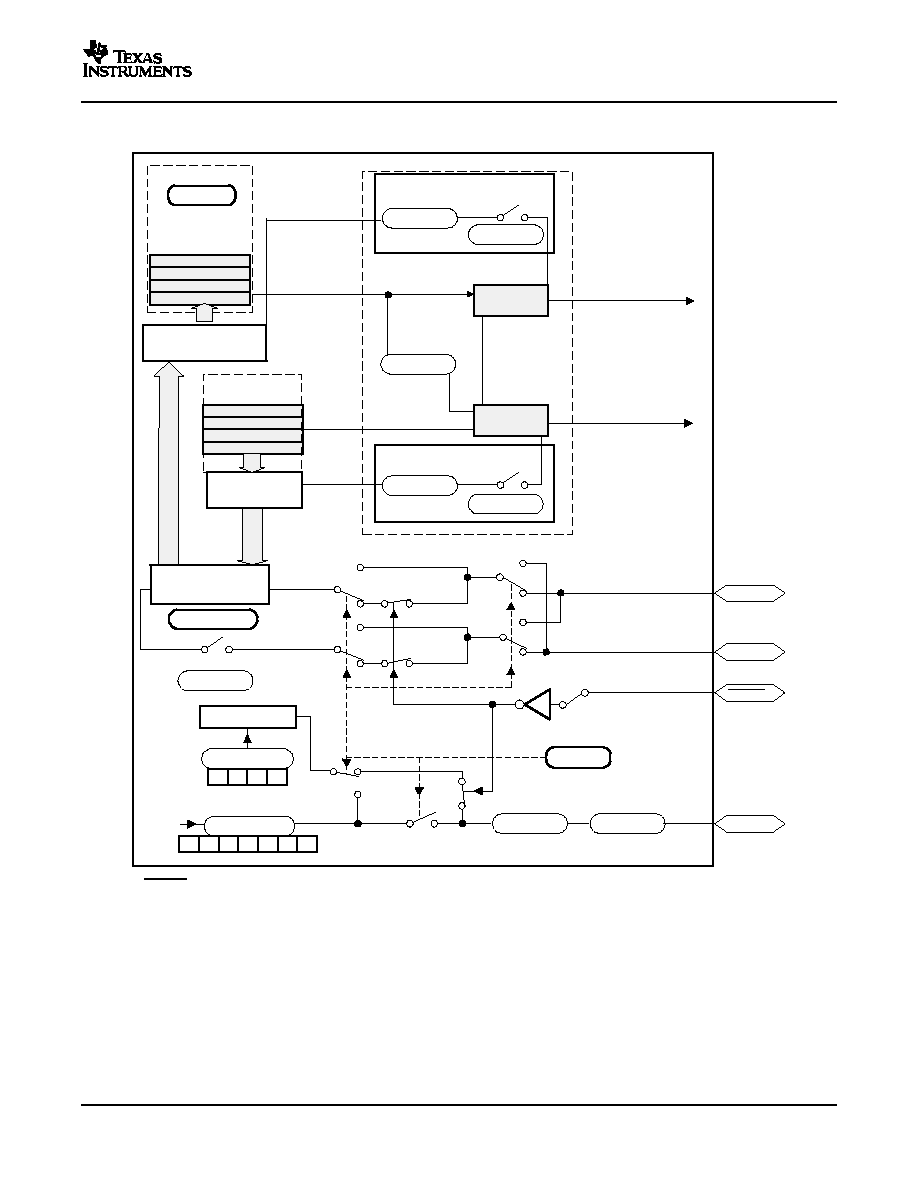
www.ti.com
S
SPICTL.0
SPI INT FLAG
SPI INT
ENA
SPISTS.6
S
Clock
Polarity
Talk
LSPCLK
4
5
6
1
2
3
0
0
1
2
3
SPI Bit Rate
State Control
SPIRXBUF
Buffer Register
Clock
Phase
Receiver
Overrun Flag
SPICTL.4
Overrun
INT ENA
SPICCR.3 - 0
SPIBRR.6 - 0
SPICCR.6
SPICTL.3
SPIDAT.15 - 0
SPICTL.1
M
S
M
Master/Slave
SPISTS.7
SPIDAT
Data Register
M
S
SPICTL.2
SPI Char
SPISIMO
SPISOMI
SPICLK
SW2
S
M
M
S
SW3
To CPU
M
SW1
SPITXBUF
Buffer Register
RX FIFO _0
RX FIFO _1
-----
RX FIFO _15
TX FIFO registers
TX FIFO _0
TX FIFO _1
-----
TX FIFO _15
RX FIFO registers
16
16
16
TX Interrupt
Logic
RX Interrupt
Logic
SPIINT/SPIRXINT
SPITXINT
SPIFFOVF FLAG
SPIFFRX.15
16
TX FIFO Interrupt
RX FIFO Interrupt
SPIRXBUF
SPITXBUF
SPIFFTX.14
SPIFFENA
SPISTE
(A)
TMS320F2809, TMS320F2808, TMS320F2806
TMS320F2802, TMS320F2801, UCD9501
TMS320C2802, TMS320C2801 Digital Signal Processors
SPRS230G ≠ OCTOBER 2003 ≠ REVISED FEBRUARY 2006
Figure 4-14
is a block diagram of the SPI in slave mode.
A.
SPISTE is driven low by the master for a slave device.
Figure 4-14. SPI Module Block Diagram (Slave Mode)
Peripherals
77

www.ti.com
4.10
Inter-Integrated Circuit (I
2
C)
TMS320F2809, TMS320F2808, TMS320F2806
TMS320F2802, TMS320F2801, UCD9501
TMS320C2802, TMS320C2801 Digital Signal Processors
SPRS230G ≠ OCTOBER 2003 ≠ REVISED FEBRUARY 2006
The 280x device contains one I
2
C Serial Port. Figure 4-15 shows how the I
2
C peripheral module interfaces
within the 280x device.
The I
2
C module has the following features:
∑
Compliance with the Philips Semiconductors I
2
C-bus specification (version 2.1):
≠
Support for 1-bit to 8-bit format transfers
≠
7-bit and 10-bit addressing modes
≠
General call
≠
START byte mode
≠
Support for multiple master-transmitters and slave-receivers
≠
Support for multiple slave-transmitters and master-receivers
≠
Combined master transmit/receive and receive/transmit mode
≠
Data transfer rate of from 10 kbps up to 400 kbps (Philips Fast-mode rate)
∑
One 16-bit receive FIFO and one 16-bit transmit FIFO
∑
One interrupt that can be used by the CPU. This interrupt can be generated as a result of one of the
following conditions:
≠
Transmit-data ready
≠
Receive-data ready
≠
Register-access ready
≠
No-acknowledgment received
≠
Arbitration lost
≠
Stop condition detected
≠
Addressed as slave
∑
An additional interrupt that can be used by the CPU when in FIFO mode
∑
Module enable/disable capability
∑
Free data format mode
78
Peripherals
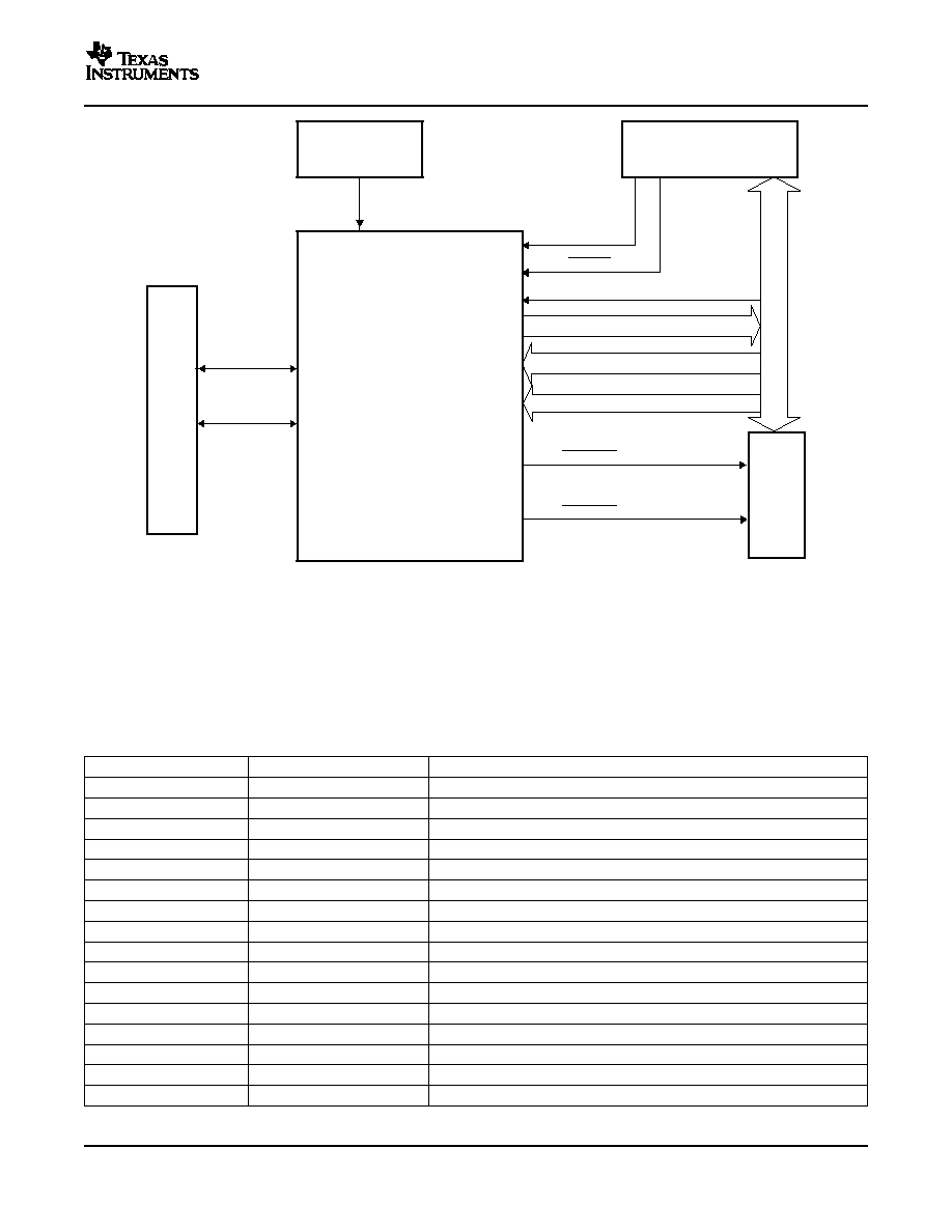
www.ti.com
SYSRS
Data[16]
SYSCLKOUT
Data[16]
Addr[16]
Control
I2CINT1A
I2CINT2A
C28X CPU
GPIO
MUX
I
2
C-A
System Control
Block
I2CAENCLK
PIE
Block
SDAA
SCLA
Peripheral Bus
TMS320F2809, TMS320F2808, TMS320F2806
TMS320F2802, TMS320F2801, UCD9501
TMS320C2802, TMS320C2801 Digital Signal Processors
SPRS230G ≠ OCTOBER 2003 ≠ REVISED FEBRUARY 2006
A.
The I
2
C registers are accessed at the SYSCLKOUT rate. The internal timing and signal waveforms of the I
2
C port are
also at the SYSCLKOUT rate.
B.
The clock enable bit (I2CAENCLK) in the PCLKCRO register turns off the clock to the I
2
C port for low power
operation. Upon reset, I2CAENCLK is clear, which indicates the peripheral internal clocks are off.
Figure 4-15. I
2
C Peripheral Module Interfaces
The registers in
Table 4-14
configure and control the I
2
C port operation.
Table 4-14. I
2
C-A Registers
NAME
ADDRESS
DESCRIPTION
I2COAR
0x7900
I
2
C own address register
I2CIER
0x7901
I
2
C interrupt enable register
I2CSTR
0x7902
I
2
C status register
I2CCLKL
0x7903
I
2
C clock low-time divider register
I2CCLKH
0x7904
I
2
C clock high-time divider register
I2CCNT
0x7905
I
2
C data count register
I2CDRR
0x7906
I
2
C data receive register
I2CSAR
0x7907
I
2
C slave address register
I2CDXR
0x7908
I
2
C data transmit register
I2CMDR
0x7909
I
2
C mode register
I2CISRC
0x790A
I
2
C interrupt source register
I2CPSC
0x790C
I
2
C prescaler register
I2CFFTX
0x7920
I
2
C FIFO transmit register
I2CFFRX
0x7921
I
2
C FIFO receive register
I2CRSR
-
I
2
C receive shift register (not accessible to the CPU)
I2CXSR
-
I
2
C transmit shift register (not accessible to the CPU)
Peripherals
79
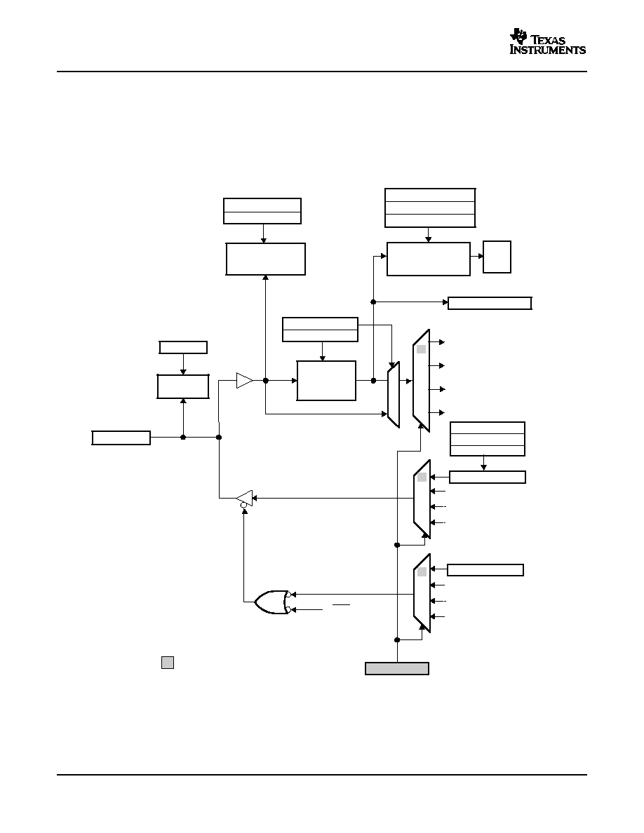
www.ti.com
4.11
GPIO MUX
GPxDAT (read)
Input
Qualification
GPxMUX1/2
High Impedance
Output Control
GPIOx pin
XRS
0 = Input, 1 = Output
Low Power
Modes Block
GPxDIR (latch)
Peripheral 2 Input
Peripheral 3 Input
Peripheral 1 Output
Peripheral 2 Output
Peripheral 3 Output
Peripheral 1 Output Enable
Peripheral 2 Output Enable
Peripheral 3 Output Enable
00
01
10
11
00
01
10
11
00
01
10
11
GPxCTRL
Peripheral 1 Input
N/C
GPxPUD
LPMCR0
Internal
Pullup
GPIOLMPSEL
GPxQSEL1/2
GPxSET
GPxDAT (latch)
GPxCLEAR
GPxTOGGLE
GPIOXINT1SEL
GPIOXINT2SEL
GPIOXNMISEL
= Default at Reset
PIE
External Interrupt
MUX
Asynchronous
path
Asynchronous path
TMS320F2809, TMS320F2808, TMS320F2806
TMS320F2802, TMS320F2801, UCD9501
TMS320C2802, TMS320C2801 Digital Signal Processors
SPRS230G ≠ OCTOBER 2003 ≠ REVISED FEBRUARY 2006
On the 280x, the GPIO MUX can multiplex up to three independent peripheral signals on a single GPIO
pin in addition to providing individual pin bit-banging IO capability. The GPIO MUX block diagram per pin
is shown in
Figure 4-16
. Because of the open drain capabilities of the I
2
C pins, the GPIO MUX block
diagram for these pins differ. See the TMS320x280x System Control and Interrupts Reference Guide
(literature number SPRU712) for details.
A.
x stands for the port, either A or B. For example, GPxDIR refers to either the GPADIR and GPBDIR register
depending on the particular GPIO pin selected.
B.
GPxDAT latch/read are accessed at the same memory location.
Figure 4-16. GPIO MUX Block Diagram
80
Peripherals
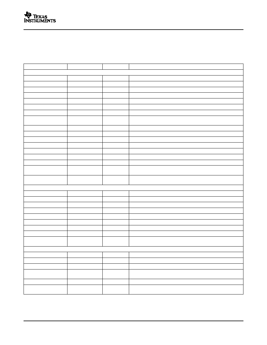
www.ti.com
TMS320F2809, TMS320F2808, TMS320F2806
TMS320F2802, TMS320F2801, UCD9501
TMS320C2802, TMS320C2801 Digital Signal Processors
SPRS230G ≠ OCTOBER 2003 ≠ REVISED FEBRUARY 2006
The 280x supports 34 GPIO pins. The GPIO control and data registers are mapped to Peripheral Frame 1
to enable 32-bit operations on the registers (along with 16-bit operations).
Table 4-15
shows the GPIO
register mapping.
Table 4-15. GPIO Registers
NAME
ADDRESS
SIZE (x16)
DESCRIPTION
GPIO CONTROL REGISTERS (EALLOW PROTECTED)
GPACTRL
0x6F80
2
GPIO A Control Register (GPIO0 to 31)
GPAQSEL1
0x6F82
2
GPIO A Qualifier Select 1 Register (GPIO0 to 15)
GPAQSEL2
0x6F84
2
GPIO A Qualifier Select 2 Register (GPIO16 to 31)
GPAMUX1
0x6F86
2
GPIO A MUX 1 Register (GPIO0 to 15)
GPAMUX2
0x6F88
2
GPIO A MUX 2 Register (GPIO16 to 31)
GPADIR
0x6F8A
2
GPIO A Direction Register (GPIO0 to 31)
GPAPUD
0x6F8C
2
GPIO A Pull Up Disable Register (GPIO0 to 31)
0x6F8E
reserved
2
0x6F8F
GPBCTRL
0x6F90
2
GPIO B Control Register (GPIO32 to 35)
GPBQSEL1
0x6F92
2
GPIO B Qualifier Select 1 Register (GPIO32 to 35)
GPBQSEL2
0x6F94
2
reserved
GPBMUX1
0x6F96
2
GPIO B MUX 1 Register (GPIO32 to 35)
GPBMUX2
0x6F98
2
reserved
GPBDIR
0x6F9A
2
GPIO B Direction Register (GPIO32 to 35)
GPBPUD
0x6F9C
2
GPIO B Pull Up Disable Register (GPIO32 to 35)
0x6F9E
reserved
2
reserved
0x6F9F
0x6FA0
reserved
32
0x6FBF
GPIO DATA REGISTERS (NOT EALLOW PROTECTED)
GPADAT
0x6FC0
2
GPIO Data Register (GPIO0 to 31)
GPASET
0x6FC2
2
GPIO Data Set Register (GPIO0 to 31)
GPACLEAR
0x6FC4
2
GPIO Data Clear Register (GPIO0 to 31)
GPATOGGLE
0x6FC6
2
GPIO Data Toggle Register (GPIO0 to 31)
GPBDAT
0x6FC8
2
GPIO Data Register (GPIO32 to 35)
GPBSET
0x6FCA
2
GPIO Data Set Register (GPIO32 to 35)
GPBCLEAR
0x6FCC
2
GPIO Data Clear Register (GPIO32 to 35)
GPBTOGGLE
0x6FCE
2
GPIO Data Toggle Register (GPIO32 to 35)
0x6FD0
reserved
16
0x6FDF
GPIO INTERRUPT AND LOW POWER MODES SELECT REGISTERS (EALLOW PROTECTED)
GPIOXINT1SEL
0x6FE0
1
XINT1 GPIO Input Select Register (GPIO0 to 31)
GPIOXINT2SEL
0x6FE1
1
XINT2 GPIO Input Select Register (GPIO0 to 31)
GPIOXNMISEL
0x6FE2
1
XNMI GPIO Input Select Register (GPIO0 to 31)
0x6FE3
reserved
5
0x6FE7
GPIOLPMSEL
0x6FE8
2
LPM GPIO Select Register (GPIO0 to 31)
0x6FEA
reserved
22
0x6FFF
Peripherals
81
www.ti.com
TMS320F2809, TMS320F2808, TMS320F2806
TMS320F2802, TMS320F2801, UCD9501
TMS320C2802, TMS320C2801 Digital Signal Processors
SPRS230G ≠ OCTOBER 2003 ≠ REVISED FEBRUARY 2006
Table 4-16. F2808 GPIO MUX Table
DEFAULT AT RESET
GPAMUX1/2
(1)
PRIMARY I/O
PERIPHERAL
PERIPHERAL
PERIPHERAL
REGISTER
FUNCTION
SELECTION 1
(2)
SELECTION 2
SELECTION 3
BITS
(GPxMUX1/2
(GPxMUX1/2 BITS = 0,1)
(GPxMUX1/2 BITS = 1,0)
(GPxMUX1/2 BITS = 1,1)
BITS = 0,0)
GPAMUX1
1-0
GPIO0
EPWM1A (O)
Reserved
(3)
Reserved
(3)
3-2
GPIO1
EPWM1B (O)
SPISIMOD (I/O)
Reserved
(3)
5-4
GPIO2
EPWM2A (O)
Reserved
(3)
Reserved
(3)
7-6
GPIO3
EPWM2B (O)
SPISOMID (I/O)
Reserved
(3)
9-8
GPIO4
EPWM3A (O)
Reserved
(3)
Reserved
(3)
11-10
GPIO5
EPWM3B (O)
SPICLKD (I/O)
ECAP1 (I/O)
13-12
GPIO6
EPWM4A (O)
EPWMSYNCI (I)
EPWMSYNCO (O)
15-14
GPIO7
EPWM4B (O)
SPISTED (I/O)
ECAP2 (I/O)
17-16
GPIO8
EPWM5A (O)
CANTXB (O)
ADCSOCAO (O)
19-18
GPIO9
EPWM5B (O)
SCITXDB (O)
ECAP3 (I/O)
21-20
GPIO10
EPWM6A (O)
CANRXB (I)
ADCSOCBO (O)
23-22
GPIO11
EPWM6B (O)
SCIRXDB (I)
ECAP4 (I/O)
25-24
GPIO12
TZ1 (I)
CANTXB (O)
SPISIMOB (I/O)
27-26
GPIO13
TZ2 (I)
CANRXB (I)
SPISOMIB (I/O)
29-28
GPIO14
TZ3 (I)
SCITXDB (O)
SPICLKB (I/O)
31-30
GPIO15
TZ4 (I)
SCIRXDB (I)
SPISTEB (I/O)
GPAMUX2
1-0
GPIO16
SPISIMOA (I/O)
CANTXB (O)
TZ5 (I)
3-2
GPIO17
SPISOMIA (I/O)
CANRXB (I)
TZ6 (I)
5-4
GPIO18
SPICLKA (I/O)
SCITXDB (O)
Reserved
(3)
7-6
GPIO19
SPISTEA (I/O)
SCIRXDB (I)
Reserved
(3)
9-8
GPIO20
EQEP1A (I)
SPISIMOC (I/O)
CANTXB (O)
11-10
GPIO21
EQEP1B (I)
SPISOMIC (I/O)
CANRXB (I)
13-12
GPIO22
EQEP1S (I/O)
SPICLKC (I/O)
SCITXDB (O)
15-14
GPIO23
EQEP1I (I/O)
SPISTEC (I/O)
SCIRXDB (I)
17-16
GPIO24
ECAP1 (I/O)
EQEP2A (I)
SPISIMOB (I/O)
19-18
GPIO25
ECAP2 (I/O)
EQEP2B (I)
SPISOMIB (I/O)
21-20
GPIO26
ECAP3 (I/O)
EQEP2I (I/O)
SPICLKB (I/O)
23-22
GPIO27
ECAP4 (I/O)
EQEP2S (I/O)
SPISTEB (I/O)
25-24
GPIO28
SCIRXDA (I)
Reserved
(3)
TZ5 (I)
27-26
GPIO29
SCITXDA (O)
Reserved
(3)
TZ6 (I)
29-28
GPIO30
CANRXA (I)
Reserved
(3)
Reserved
(3)
31-30
GPIO31
CANTXA (O)
Reserved
(3)
Reserved
(3)
GPBMUX1
1-0
GPIO32
SDAA (I/OC)
EPWMSYNCI (I)
ADCSOCAO (O)
3-2
GPIO33
SCLA (I/OC)
EPWMSYNCO (O)
ADCSOCBO (O)
5-4
GPIO34
Reserved
(3)
Reserved
(3)
Reserved
(3)
(1)
GPxMUX1/2 refers to the appropriate MUX register for the pin; GPAMUX1, GPAMUX2 or GPBMUX1.
(2)
This table pertains to the 2808 device. Some peripherals may not be available in the 2809, 2806, 2802, or 2801 devices. See the pin
descriptions for more detail.
(3)
The word "Reserved" means that there is no peripheral assigned to this GPxMUX1/2 register setting. Should it be selected, the state of
the pin will be undefined and the pin may be driven. This selection is a reserved configuration for future expansion.
Peripherals
82
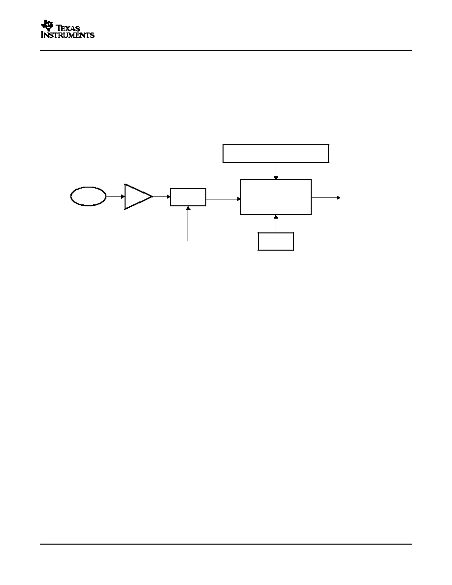
www.ti.com
GPyCTRL Reg
SYNC
SYSCLKOUT
Qualification
Input Signal
Qualified By 3
or 6 Samples
GPIOx
Time between samples
GPxQSEL
Number of Samples
TMS320F2809, TMS320F2808, TMS320F2806
TMS320F2802, TMS320F2801, UCD9501
TMS320C2802, TMS320C2801 Digital Signal Processors
SPRS230G ≠ OCTOBER 2003 ≠ REVISED FEBRUARY 2006
The user can select the type of input qualification for each GPIO pin via the GPxQSEL1/2 registers from
four choices:
∑
Synchronization To SYSCLKOUT Only (GPxQSEL1/2=0,0): This is the default mode of all GPIO pins
at reset and it simply synchronizes the input signal to the system clock (SYSCLKOUT).
∑
Qualification Using Sampling Window (GPxQSEL1/2=0,1 and 1,0): In this mode the input signal, after
synchronization to the system clock (SYSCLKOUT), is qualified by a specified number of cycles before
the input is allowed to change.
Figure 4-17. Qualification Using Sampling Window
∑
The sampling period is specified by the QUALPRD bits in the GPxCTRL register and is configurable in
groups of 8 signals. It specifies a multiple of SYSCLKOUT cycles for sampling the input signal. The
sampling window is either 3-samples or 6-samples wide and the output is only changed when ALL
samples are the same (all 0s or all 1s) as shown in Figure 4-18 (for 6 sample mode).
∑
No Synchronization (GPxQSEL1/2=1,1): This mode is used for peripherals where synchronization is
not required (synchronization is performed within the peripheral).
Due to the multi-level multiplexing that is required on the 280x device, there may be cases where a
peripheral input signal can be mapped to more then one GPIO pin. Also, when an input signal is not
selected, the input signal will default to either a 0 or 1 state, depending on the peripheral.
Peripherals
83

www.ti.com
5
Device Support
5.1
Device and Development Support Tool Nomenclature
TMS320F2809, TMS320F2808, TMS320F2806
TMS320F2802, TMS320F2801, UCD9501
TMS320C2802, TMS320C2801 Digital Signal Processors
SPRS230G ≠ OCTOBER 2003 ≠ REVISED FEBRUARY 2006
Texas Instruments (TI) offers an extensive line of development tools for the C28xTM generation of DSPs,
including tools to evaluate the performance of the processors, generate code, develop algorithm
implementations, and fully integrate and debug software and hardware modules.
The following products support development of 280x-based applications:
Software Development Tools
∑
Code Composer StudioTM Integrated Development Environment (IDE)
≠
C/C++ Compiler
≠
Code generation tools
≠
Assembler/Linker
≠
Cycle Accurate Simulator
∑
Application algorithms
∑
Sample applications code
Hardware Development Tools
∑
2808 eZdspTM
∑
JTAG-based emulators - SPI515, XDS510PP, XDS510PP Plus, XDS510USBTM
∑
Universal 5-V dc power supply
∑
Documentation and cables
To designate the stages in the product development cycle, TI assigns prefixes to the part numbers of all
TMS320TM DSP devices and support tools. Each TMS320TM DSP commercial family member has one of
three prefixes: TMX, TMP, or TMS (e.g., TMS320F2808). Texas Instruments recommends two of three
possible prefix designators for its support tools: TMDX and TMDS. These prefixes represent evolutionary
stages of product development from engineering prototypes (TMX/TMDX) through fully qualified
production devices/tools (TMS/TMDS).
Device development evolutionary flow:
TMX
Experimental device that is not necessarily representative of the final device's electrical
specifications
TMP
Final silicon die that conforms to the device's electrical specifications but has not completed
quality and reliability verification
TMS
Fully qualified production device
Support tool development evolutionary flow:
TMDX
Development-support product that has not yet completed Texas Instruments internal qualification
testing
TMDS
Fully qualified development-support product
TMX and TMP devices and TMDX development-support tools are shipped against the following
disclaimer:
"Developmental product is intended for internal evaluation purposes."
TMS devices and TMDS development-support tools have been characterized fully, and the quality and
reliability of the device have been demonstrated fully. TI's standard warranty applies.
84
Device Support

www.ti.com
PREFIX
TMS
320
F
2808
PZ
TMX = Experimental Device
TMP = Prototype Device
TMS = Qualified Device
DEVICE FAMILY
320 = TMS320
E
DSP Family
TECHNOLOGY
PACKAGE TYPE
PZ
= 100-Pin Low-Profile Quad
Flatpack (LQFP)
GGM = 100-Ball Ball Grid Array (BGA)
ZGM = 100-Ball Lead-Free BGA
F = Flash EEPROM
(1.8-V Core/3.3-V I/O)
DEVICE
2809
2808
2806
2802
2801
TEMPERATURE RANGE
A
= ≠40
5
C to 85
5
C
S
= ≠40
5
C to 125
5
C
Q
= ≠40
5
C to 125
5
C -- Q100 Fault Grading
A
PREFIX
X
UCD
9501
PZ
X
= Experimental Device
Blank = Qualified Device
DEVICE FAMILY
UCD =
UCD Family
PACKAGE TYPE
PZ
= 100-Pin Low-Profile Quad
Flatpack (LQFP)
DEVICE
TEMPERATURE RANGE
A
= ≠40
5
C to 85
5
C
A
TMS320F2809, TMS320F2808, TMS320F2806
TMS320F2802, TMS320F2801, UCD9501
TMS320C2802, TMS320C2801 Digital Signal Processors
SPRS230G ≠ OCTOBER 2003 ≠ REVISED FEBRUARY 2006
Predictions show that prototype devices (TMX or TMP) have a greater failure rate than the standard
production devices. Texas Instruments recommends that these devices not be used in any production
system because their expected end-use failure rate still is undefined. Only qualified production devices are
to be used.
TI device nomenclature also includes a suffix with the device family name. This suffix indicates the
package type (for example, PBK) and temperature range (for example, A).
Figure 5-1
provides a legend
for reading the complete device name for any family member.
Figure 5-1. Example of TMS320x280x Device Nomenclature
Figure 5-2. Example of UCD Device Nomenclature
Device Support
85

www.ti.com
5.2
Documentation Support
TMS320F2809, TMS320F2808, TMS320F2806
TMS320F2802, TMS320F2801, UCD9501
TMS320C2802, TMS320C2801 Digital Signal Processors
SPRS230G ≠ OCTOBER 2003 ≠ REVISED FEBRUARY 2006
Extensive documentation supports all of the TMS320TM DSP family generations of devices from product
announcement through applications development. The types of documentation available include: data
sheets and data manuals, with design specifications; and hardware and software applications.
TMS320x280x device reference guides are applicable to the UCD9501 device as well. Useful reference
documentation includes:
SPRU051:
TMS320x281x, 280x Serial Communication Interface (SCI) Reference Guide
Describes the SCI, which is a two-wire asynchronous serial port, commonly known as a
UART. The SCI modules support digital communications between the CPU and other
asynchronous peripherals that use the standard non-return-to-zero (NRZ) format.
SPRU059:
TMS320x281x, 280x Serial Peripheral Interface (SPI) Reference Guide
Describes the SPI - a high-speed synchronous serial input/output (I/O) port that allows a
serial bit stream of programmed length (one to sixteen bits) to be shifted into and out of the
device at a programmed bit-transfer rate. The SPI is used for communications between the
DSP controller and external peripherals or another controller.
SPRU074:
TMS320x281x, 280x Enhanced Controller Area Network (eCAN) Reference Guide
Describes the eCAN that uses established protocol to communicate serially with other
controllers in electrically noisy environments. With 32 fully configurable mailboxes and
time-stamping
feature,
the
eCAN
module
provides
a
versatile
and
robust
serial
communication interface. The eCAN module implemented in the 281x DSP is compatible
with the CAN 2.0B standard (active).
SPRU430:
TMS320C28x DSP CPU and Instruction Set Reference Guide
Describes the central processing unit (CPU) and the assembly language instructions of the
TMS320C28x fixed-point digital signal processors (DSPs). It also describes emulation
features available on these DSPs.
SPRU513:
TMS320C28x Assembly Language Tools User's Guide
Describes the assembly language tools (assembler and other tools used to develop
assembly language code), assembler directives, macros, common object file format, and
symbolic debugging directives for the TMS320C28x device.
SPRU514:
TMS320C28x Optimizing C Compiler User's Guide
describes the TMS320C28x C/C++ compiler. This compiler accepts ANSI standard C/C++
source code and produces TMS320 DSP assembly language source code for the
TMS320C28x device.
SPRU566:
TMS320x281x, 280x Peripheral Reference Guide
Describes the peripheral reference guides of the 28x digital signal processors (DSPs).
SPRU608:
The TMS320C28x Instruction Set Simulator Technical Overview
Describes the simulator, available within the Code Composer Studio for TMS320C2000 IDE,
that simulates the instruction set of the C28x core.
SPRU625:
TMS320C28x DSP/BIOS Application Programming Interface (API) Reference Guide
Describes development using DSP/BIOS.
SPRU712:
TMS320x280x System Control and Interrupts Reference Guide
Describes the various interrupts and system control features of the 280x digital signal
processors (DSPs).
SPRU716:
TMS320x280x Analog-to-Digital Converter (ADC) Reference Guide
Describes the ADC module. The module is a 12-bit pipelined ADC. The analog circuits of
this converter, referred to as the core in this document, include the front-end analog
86
Device Support

www.ti.com
TMS320F2809, TMS320F2808, TMS320F2806
TMS320F2802, TMS320F2801, UCD9501
TMS320C2802, TMS320C2801 Digital Signal Processors
SPRS230G ≠ OCTOBER 2003 ≠ REVISED FEBRUARY 2006
multiplexers (MUXs), sample-and-hold (S/H) circuits, the conversion core, voltage regulators,
and other analog supporting circuits. Digital circuits, referred to as the wrapper in this
document, include programmable conversion sequencer, result registers, interface to analog
circuits, interface to device peripheral bus, and interface to other on-chip modules.
SPRU722:
TMS320x280x Boot ROM Reference Guide
Describes the purpose and features of the bootloader (factory-programmed boot-loading
software). It also describes other contents of the device on-chip boot ROM and identifies
where all of the information is located within that memory.
SPRU790:
TMS320x280x Enhanced Quadrature Encoder Pulse (eQEP) Reference Guide
Describes the eQEP module, which is used for interfacing with a linear or rotary incremental
encoder to get position, direction, and speed information from a rotating machine in high
performance motion and position control systems. It includes the module description and
registers.
SPRU791:
TMS320x280x Enhanced Pulse Width Modulator (ePWM) Module Reference Guide
The PWM peripheral is an essential part of controlling many of the power related systems
found in both commercial and industrial equipments. This guide describes the main areas
that include digital motor control, switch mode power supply control, UPS (uninterruptible
power supplies), and other forms of power conversion. The PWM peripheral can be
considered as performing a DAC function, where the duty cycle is equivalent to a DAC
analog value, it is sometimes referred to as a Power DAC.
SPRU807:
TMS320x280x Enhanced Capture (eCAP) Module Reference Guide
Describes the enhanced capture module. It includes the module description and registers.
SPRU924:
High-Resolution Pulse Width Modulator (HRPWM)
describes the operation of the
high-resolution extension to the pulse width modulator (HRPWM)
SPRA550:
3.3 V DSP for Digital Motor Control
describes a scenario of a 3.3-V-only motor controller
indicating that for most applications, no significant issue of interfacing between 3.3 V and 5 V
exists. On-chip 3.3-V analog-to-digital converter (ADC) versus 5-V ADC is also discussed.
Guidelines for component layout and printed circuit board (PCB) design that can reduce
system noise and EMI effects are summarized.
A series of DSP textbooks is published by Prentice-Hall and John Wiley & Sons to support digital signal
processing research and education. The TMS320 DSP newsletter, Details on Signal Processing, is
published quarterly and distributed to update TMS320 DSP customers on product information.
Updated information on the TMS320 DSP controllers can be found on the worldwide web at:
http://www.ti.com.
To
send
comments
regarding
this
data
manual
(literature
number
SPRS230),
use
the
comments@books.sc.ti.com email address, which is a repository for feedback. For questions and support,
contact the Product Information Center listed at the http://www.ti.com/sc/docs/pic/home.htm site.
Device Support
87
www.ti.com
6
Electrical Specifications
6.1
Absolute Maximum Ratings
(1) (2)
TMS320F2809, TMS320F2808, TMS320F2806
TMS320F2802, TMS320F2801, UCD9501
TMS320C2802, TMS320C2801 Digital Signal Processors
SPRS230G ≠ OCTOBER 2003 ≠ REVISED FEBRUARY 2006
This section provides the absolute maximum ratings and the recommended operating conditions for the
TMS320F280x DSPs.
NOTE
Information/data on TMS320F2809 is PRODUCT PREVIEW.
PRODUCT PREVIEW information concerns products in the formative or design phase of
development. Characteristic data and other specifications are design goals. Texas
Instruments reserves the right to change or discontinue these products without notice.
Unless otherwise noted, the list of absolute maximum ratings are specified over operating temperature ranges.
Supply voltage range, V
DDIO
, V
DD3VFL
with respect to V
SS
- 0.3 V to 4.6 V
Supply voltage range, V
DDA2
, V
DDAIO
with respect to V
SSA
- 0.3 V to 4.6 V
Supply voltage range, V
DD
with respect to V
SS
- 0.3 V to 2.5 V
Supply voltage range, V
DD1A18
, V
DD2A18
with respect to V
SSA
- 0.3 V to 2.5 V
Supply voltage range, V
SSA2
, V
SSAIO
, V
SS1AGND
, V
SS2AGND
with respect to V
SS
- 0.3 V to 0.3 V
Input voltage range, V
IN
- 0.3 V to 4.6 V
Output voltage range, V
O
- 0.3 V to 4.6 V
Input clamp current, I
IK
(V
IN
< 0 or V
IN
> V
DDIO
)
(3)
±
20 mA
Output clamp current, I
OK
(V
O
< 0 or V
O
> V
DDIO
)
±
20 mA
Operating ambient temperature ranges,
T
A
: A version (GGM, PZ)
(4)
- 40
∞
C to 85
∞
C
T
A
: S version (GGM, PZ)
(4)
- 40
∞
C to 125
∞
C
T
A
: Q version ( PZ)
(4)
- 40
∞
C to 125
∞
C
Junction temperature range, T
j
(4)
- 40
∞
C to 150
∞
C
Storage temperature range, T
stg
(4)
- 65
∞
C to 150
∞
C
(1)
Stresses beyond those listed under Absolute Maximum Ratings may cause permanent damage to the device. These are stress ratings
only, and functional operation of the device at these or any other conditions beyond those indicated under
Section 6.2
is not implied.
Exposure to absolute-maximum-rated conditions for extended periods may affect device reliability.
(2)
All voltage values are with respect to V
SS
, unless otherwise noted.
(3)
Continuous clamp current per pin is
±
2 mA. This includes the analog inputs which have an internal clamping circuit that clamps the
voltage to a diode drop above V
DDA2
or below V
SSA2
.
(4)
Long-term high-temperature storage and/or extended use at maximum temperature conditions may result in a reduction of overall device
life. For additional information, see IC Package Thermal Metrics Application Report (literature number SPRA953) and Reliability Data for
TMS320LF24x and TMS320F281x Devices Application Report (literature number SPRA963)
Electrical Specifications
88
www.ti.com
6.2
Recommended Operating Conditions
6.3
Electrical Characteristics
TMS320F2809, TMS320F2808, TMS320F2806
TMS320F2802, TMS320F2801, UCD9501
TMS320C2802, TMS320C2801 Digital Signal Processors
SPRS230G ≠ OCTOBER 2003 ≠ REVISED FEBRUARY 2006
over operating free-air temperature range (unless otherwise noted)
MIN
NOM
MAX
UNIT
Device supply voltage, I/O, V
DDIO
3.14
3.3
3.47
V
Device supply voltage CPU, V
DD
1.71
1.8
1.89
V
Supply ground, V
SS
, V
SSIO
0
V
ADC supply voltage (3.3 V), V
DDA2
, V
DDAIO
3.14
3.3
3.47
V
ADC supply voltage (1.8 V), V
DD1A18
, V
DD2A18
1.71
1.8
1.89
V
Flash supply voltage, V
DD3VFL
3.14
3.3
3.47
V
Device clock frequency (system clock), f
SYSCLKOUT
2
100
MHz
High-level input voltage, V
IH
2
V
DDIO
V
Low-level input voltage, V
IL
0.8
All I/Os except Group 2
-4
mA
High-level output source current, V
OH
= 2.4 V, I
OH
Group 2
(1)
-8
All I/Os except Group 2
4
mA
Low-level output sink current, V
OL
= V
OL
MAX, I
OL
Group 2
(1)
8
A version
-40
85
Ambient temperature, T
A
S version
-40
125
∞
C
Q version
-40
125
(1)
Group 2 pins are as follows: GPIO28, GPIO29, GPIO30, GPIO31, TDO, XCLKOUT, EMU0, and EMU1
over recommended operating conditions (unless otherwise noted)
PARAMETER
TEST CONDITIONS
MIN
TYP
MAX
UNIT
I
OH
= I
OH
MAX
2.4
V
OH
High-level output voltage
V
I
OH
= 50
µ
A
V
DDIO
- 0.2
V
OL
Low-level output voltage
I
OL
= I
OL
MAX
0.4
V
Pin with pullup
V
DDIO
= 3.3 V, V
IN
= 0 V
All I/Os (including XRS)
-80
-140
-190
enabled
Input current
I
IL
µ
A
(low level)
Pin with pulldown
V
DDIO
= 3.3 V, V
IN
= 0 V
±
2
enabled
Pin with pullup
V
DDIO
= 3.3 V, V
IN
= V
DDIO
±
2
enabled
Input current
Pin with pulldown
I
IH
V
DDIO
= 3.3 V, V
IN
= V
DDIO
(F280x)
28
50
80
µ
A
(high level)
enabled
Pin with pulldown
V
DDIO
= 3.3 V, V
IN
= V
DDIO
(C280x)
80
140
190
enabled
Output current, pullup or
I
OZ
V
O
= V
DDIO
or 0 V
±
2
µ
A
pulldown disabled
C
I
Input capacitance
2
pF
Electrical Specifications
89

www.ti.com
6.4
Current Consumption
TMS320F2809, TMS320F2808, TMS320F2806
TMS320F2802, TMS320F2801, UCD9501
TMS320C2802, TMS320C2801 Digital Signal Processors
SPRS230G ≠ OCTOBER 2003 ≠ REVISED FEBRUARY 2006
Table 6-1. TMS320F2808 Current Consumption by Power-Supply Pins at 100-MHz SYSCLKOUT
I
DD
I
DDIO
(1)
I
DD3VFL
I
DDA18
(2)
I
DDA33
(3)
MODE
TEST CONDITIONS
TYP
(4)
MAX
TYP
(4)
MAX
TYP
MAX
TYP
(4)
MAX
TYP
(4)
MAX
The following peripheral
clocks are enabled:
∑
ePWM1/2/3/4/5/6
∑
eCAP1/2/3/4
∑
eQEP1/2
∑
eCAN-A
∑
SCI-A/B
∑
SPI-A
∑
ADC
∑
I
2
C
Operational
195 mA
230 mA
15 mA
27 mA
35 mA
40 mA
30 mA
38 mA
1.5 mA
2 mA
All PWM pins are toggled
(Flash)
at 100 kHz.
All I/O pins are left
unconnected.
Data is continuously
transmitted out of the
SCI-A, SCI-B, and
eCAN-A ports. The
hardware multiplier is
exercised.
Code is running out of
flash with 3 wait states.
XCLKOUT is turned off.
Flash is powered down.
XCLKOUT is turned off.
The following peripheral
clocks are enabled:
IDLE
75 mA
90 mA
500
µ
A
2 mA
2
µ
A
10
µ
A
5
µ
A
50
µ
A
15
µ
A
30
µ
A
∑
eCAN-A
∑
SCI-A
∑
SPI-A
∑
I
2
C
Flash is powered down.
STANDBY
6 mA
12 mA
100
µ
A
500
µ
A
2
µ
A
10
µ
A
5
µ
A
50
µ
A
15
µ
A
30
µ
A
Peripheral clocks are off.
Flash is powered down.
HALT
Peripheral clocks are off.
70
µ
A
60
µ
A
120
µ
A
2
µ
A
10
µ
A
5
µ
A
50
µ
A
15
µ
A
30
µ
A
Input clock is disabled.
(1)
I
DDIO
current is dependent on the electrical loading on the I/O pins.
(2)
I
DDA18
includes current into V
DD1A18
and V
DD2A18
pins. In order to realize the I
DDA18
currents shown for IDLE, STANDBY, and HALT,
clock to the ADC module must be turned off explicitly by writing to the PCLKCR0 register.
(3)
I
DDA33
includes current into V
DDA2
and V
DDAIO
pins.
(4)
The TYP numbers are applicable over room temperature and nominal voltage.
CAUTION
The peripheral - I/O multiplexing implemented in the 280x devices prevents all
available peripherals from being used at the same time. This is because more than
one peripheral function may share an I/O pin. It is, however, possible to turn on the
clocks to all the peripherals at the same time, although such a configuration is not
useful. If this is done, the current drawn by the device will be more than the numbers
specified in the current consumption tables.
Electrical Specifications
90

www.ti.com
TMS320F2809, TMS320F2808, TMS320F2806
TMS320F2802, TMS320F2801, UCD9501
TMS320C2802, TMS320C2801 Digital Signal Processors
SPRS230G ≠ OCTOBER 2003 ≠ REVISED FEBRUARY 2006
Table 6-2. TMS320F2806 Current Consumption by Power-Supply Pins at 100-MHz SYSCLKOUT
I
DD
I
DDIO
(1)
I
DD3VFL
I
DDA18
(2)
I
DDA33
(3)
MODE
TEST CONDITIONS
TYP
(4)
MAX
TYP
(4)
MAX
TYP
(4)
MAX
TYP
(4)
MAX
TYP
(4)
MAX
The following peripheral
clocks are enabled:
∑
ePWM1/2/3/4/5/6
∑
eCAP1/2/3/4
∑
eQEP1/2
∑
eCAN-A
∑
SCI-A/B
∑
SPI-A
∑
ADC
Operational
∑
I
2
C
195 mA
230 mA
15 mA
27 mA
35 mA
40 mA
30 mA
38 mA
1.5 mA
2 mA
(Flash)
All PWM pins are toggled at
100 kHz.
All I/O pins are left
unconnected.
Data is continuously
transmitted out of the
SCI-A, SCI-B, and eCAN-A
ports. The hardware
multiplier is exercised.
Code is running out of flash
with 3 wait states.
XCLKOUT is turned off
Flash is powered down.
XCLKOUT is turned off.
The following peripheral
clocks are enabled:
IDLE
75 mA
90 mA
500
µ
A
2 mA
2
µ
A
10
µ
A
5
µ
A
50
µ
A
15
µ
A
30
µ
A
∑
eCAN-A
∑
SCI-A
∑
SPI-A
∑
I
2
C
Flash is powered down.
STANDBY
6 mA
12 mA
100
µ
A
500
µ
A
2
µ
A
10
µ
A
5
µ
A
50
µ
A
15
µ
A
30
µ
A
Peripheral clocks are off.
Flash is powered down.
HALT
Peripheral clocks are off.
70
µ
A
60
µ
A
120
µ
A
2
µ
A
10
µ
A
5
µ
A
50
µ
A
15
µ
A
30
µ
A
Input clock is disabled.
(1)
I
DDIO
current is dependent on the electrical loading on the I/O pins.
(2)
I
DDA18
includes current into V
DD1A18
and V
DD2A18
pins. In order to realize the I
DDA18
currents shown for IDLE, STANDBY, and HALT,
clock to the ADC module must be turned off explicitly by writing to the PCLKCR0 register.
(3)
I
DDA33
includes current into V
DDA2
and V
DDAIO
pins.
(4)
The TYP numbers are applicable over room temperature and nominal voltage.
CAUTION
The peripheral - I/O multiplexing implemented in the 280x devices prevents all
available peripherals from being used at the same time. This is because more than
one peripheral function may share an I/O pin. It is, however, possible to turn on the
clocks to all the peripherals at the same time, although such a configuration is not
useful. If this is done, the current drawn by the device will be more than the numbers
specified in the current consumption tables.
Electrical Specifications
91

www.ti.com
TMS320F2809, TMS320F2808, TMS320F2806
TMS320F2802, TMS320F2801, UCD9501
TMS320C2802, TMS320C2801 Digital Signal Processors
SPRS230G ≠ OCTOBER 2003 ≠ REVISED FEBRUARY 2006
Table 6-3. TMS320F2802, TMS320F2801/UCD9501 Current Consumption by Power-Supply Pins at
100-MHz SYSCLKOUT
I
DD
I
DDIO
(1)
I
DD3VFL
I
DDA18
(2)
I
DDA33
(3)
MODE
TEST CONDITIONS
TYP
(4)
MAX
TYP
(4)
MAX
TYP
(4)
MAX
TYP
(4)
MAX
TYP
(4)
MAX
The following peripheral
clocks are enabled:
∑
ePWM1/2/3
∑
eCAP1/2
∑
eQEP1
∑
eCAN-A
∑
SCI-A
∑
SPI-A
∑
ADC
Operational
∑
I
2
C
180 mA
210 mA
15 mA
27 mA
35 mA
40 mA
30 mA
38 mA
1.5 mA
2 mA
(Flash)
All PWM pins are toggled at
100 kHz.
All I/O pins are left
unconnected.
Data is continuously
transmitted out of the SCI-A,
SCI-B, and eCAN-A ports.
The hardware multiplier is
exercised.
Code is running out of flash
with 3 wait states.
XCLKOUT is turned off.
Flash is powered down.
XCLKOUT is turned off.
The following peripheral
clocks are enabled:
IDLE
75 mA
90 mA
500
µ
A
2 mA
2
µ
A
10
µ
A
5
µ
A
50
µ
A
15
µ
A
30
µ
A
∑
eCAN-A
∑
SCI-A
∑
SPI-A
∑
I
2
C
Flash is powered down.
STANDBY
6 mA
12 mA
100
µ
A
500
µ
A
2
µ
A
10
µ
A
5
µ
A
50
µ
A
15
µ
A
30
µ
A
Peripheral clocks are off.
Flash is powered down.
HALT
Peripheral clocks are off.
70
µ
A
60
µ
A
120
µ
A
2
µ
A
10
µ
A
5
µ
A
50
µ
A
15
µ
A
30
µ
A
Input clock is disabled.
(1)
I
DDIO
current is dependent on the electrical loading on the I/O pins.
(2)
I
DDA18
includes current into V
DD1A18
and V
DD2A18
pins. In order to realize the I
DDA18
currents shown for IDLE, STANDBY, and HALT,
clock to the ADC module must be turned off explicitly by writing to the PCLKCR0 register.
(3)
I
DDA33
includes current into V
DDA2
and V
DDAIO
pins.
(4)
The TYP numbers are applicable over room temperature and nominal voltage.
CAUTION
The peripheral - I/O multiplexing implemented in the 280x devices prevents all
available peripherals from being used at the same time. This is because more than
one peripheral function may share an I/O pin. It is, however, possible to turn on the
clocks to all the peripherals at the same time, although such a configuration is not
useful. If this is done, the current drawn by the device will be more than the numbers
specified in the current consumption tables.
Electrical Specifications
92

www.ti.com
TMS320F2809, TMS320F2808, TMS320F2806
TMS320F2802, TMS320F2801, UCD9501
TMS320C2802, TMS320C2801 Digital Signal Processors
SPRS230G ≠ OCTOBER 2003 ≠ REVISED FEBRUARY 2006
Table 6-4. TMS320C2802, TMS320C2801 Current Consumption by Power-Supply Pins at
100-MHz SYSCLKOUT
I
DD
I
DDIO
(1)
I
DDA18
(2)
I
DDA33
(3)
MODE
TEST CONDITIONS
TYP
(4)
MAX
TYP
(4)
MAX
TYP
(4)
MAX
TYP
(4)
MAX
The following peripheral clocks
are enabled:
∑
ePWM1/2/3
∑
eCAP1/2
∑
eQEP1
∑
eCAN-A
∑
SCI-A
∑
SPI-A
∑
ADC
Operational
150 mA
165 mA
5 mA
10 mA
30 mA
38 mA
1.5 mA
2 mA
(ROM)
∑
I
2
C
All PWM pins are toggled at
100 kHz.
All I/O pins are left unconnected.
Data is continuously transmitted
out of the SCI-A, SCI-B, and
eCAN-A ports. The hardware
multiplier is exercised.
Code is running out of ROM with
3 wait states.
XCLKOUT is turned off.
XCLKOUT is turned off.
The following peripheral clocks
are enabled:
∑
eCAN-A
IDLE
75 mA
90 mA
500
µ
A
2 mA
5
µ
A
50
µ
A
15
µ
A
30
µ
A
∑
SCI-A
∑
SPI-A
∑
I
2
C
STANDBY
Peripheral clocks are off.
6 mA
12 mA
100
µ
A
500
µ
A
5
µ
A
50
µ
A
15
µ
A
30
µ
A
Peripheral clocks are off.
HALT
70
µ
A
80
µ
A
120
µ
A
5
µ
A
50
µ
A
15
µ
A
30
µ
A
Input clock is disabled.
(1)
I
DDIO
current is dependent on the electrical loading on the I/O pins.
(2)
I
DDA18
includes current into V
DD1A18
and V
DD2A18
pins. In order to realize the I
DDA18
currents shown for IDLE, STANDBY, and HALT,
clock to the ADC module must be turned off explicitly by writing to the PCLKCR0 register.
(3)
I
DDA33
includes current into V
DDA2
and V
DDAIO
pins.
(4)
The TYP numbers are applicable over room temperature and nominal voltage.
CAUTION
The peripheral - I/O multiplexing implemented in the 280x devices prevents all
available peripherals from being used at the same time. This is because more than
one peripheral function may share an I/O pin. It is, however, possible to turn on the
clocks to all the peripherals at the same time, although such a configuration is not
useful. If this is done, the current drawn by the device will be more than the numbers
specified in the current consumption tables.
Electrical Specifications
93

www.ti.com
6.4.1
Reducing Current Consumption
TMS320F2809, TMS320F2808, TMS320F2806
TMS320F2802, TMS320F2801, UCD9501
TMS320C2802, TMS320C2801 Digital Signal Processors
SPRS230G ≠ OCTOBER 2003 ≠ REVISED FEBRUARY 2006
280x devices have a richer peripheral mix compared to the 281x family. While the McBSP has been
removed, the following new peripherals have been added on the 280x:
∑
3 SPI modules
∑
1 CAN module
∑
1 I
2
C module
The two event manager modules of the 281x have been enhanced and replaced with separate ePWM (6),
eCAP (4) and eQEP (2) modules, providing tremendous flexibility in applications. Like 281x, 280x DSPs
incorporate a unique method to reduce the device current consumption. Since each peripheral unit has an
individual clock-enable bit, significant reduction in current consumption can be achieved by turning off the
clock to any peripheral module that is not used in a given application. Furthermore, any one of the three
low-power modes could be taken advantage of to reduce the current consumption even further.
Table 6-5
indicates the typical reduction in current consumption achieved by turning off the clocks.
Table 6-5. Typical Current Consumption by Various
Peripherals (at 100 MHz)
(1)
PERIPHERAL
I
DD
CURRENT
MODULE
REDUCTION (mA)
ADC
8
(2)
I
2
C
5
eQEP
5
ePWM
5
eCAP
2
SCI
4
SPI
5
eCAN
11
(1)
All peripheral clocks are disabled upon reset. Writing to/reading
from peripheral registers is possible only after the peripheral clocks
are turned on.
(2)
This number represents the current drawn by the digital portion of
the ADC module. Turning off the clock to the ADC module results in
the elimination of the current drawn by the analog portion of the
ADC (I
DDA18
) as well.
NOTE
The baseline I
DD
current (current when the core is executing a dummy loop with no
peripherals enabled) is 110 mA, typical. To arrive at the I
DD
current for a given application,
the current-drawn by the peripherals (enabled by that application) must be added to the
baseline I
DD
current.
Electrical Specifications
94
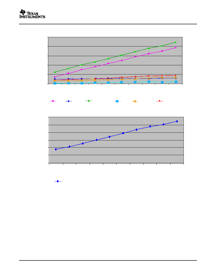
www.ti.com
6.4.2
Current Consumption Graphs
0.0
50.0
100.0
150.0
200.0
250.0
10
20
30
40
50
60
70
80
90
100
SYSCLKOUT (MHz)
Current (mA)
IDD
IDDA18
IDDIO
IDD3VFL
3.3-V current
1.8-V current
0.0
100.0
200.0
300.0
400.0
500.0
600.0
10
20
30
40
50
60
70
80
90
100
SYSCLKOUT (MHz)
Device Power (mW)
TOTAL POWER
TMS320F2809, TMS320F2808, TMS320F2806
TMS320F2802, TMS320F2801, UCD9501
TMS320C2802, TMS320C2801 Digital Signal Processors
SPRS230G ≠ OCTOBER 2003 ≠ REVISED FEBRUARY 2006
Figure 6-1. Typical Operational Current Versus Frequency (F2808)
Figure 6-2. Typical Operational Power Versus Frequency (F2808)
Electrical Specifications
95

www.ti.com
6.5
Timing Parameter Symbology
6.5.1
General Notes on Timing Parameters
TMS320F2809, TMS320F2808, TMS320F2806
TMS320F2802, TMS320F2801, UCD9501
TMS320C2802, TMS320C2801 Digital Signal Processors
SPRS230G ≠ OCTOBER 2003 ≠ REVISED FEBRUARY 2006
Timing parameter symbols used are created in accordance with JEDEC Standard 100. To shorten the
symbols, some of the pin names and other related terminology have been abbreviated as follows:
Lowercase subscripts and their
Letters and symbols and their
meanings:
meanings:
a
access time
H
High
c
cycle time (period)
L
Low
d
delay time
V
Valid
Unknown, changing, or don't
f
fall time
X
care level
h
hold time
Z
High impedance
r
rise time
su
setup time
t
transition time
v
valid time
w
pulse duration (width)
All output signals from the 28x devices (including XCLKOUT) are derived from an internal clock such that
all output transitions for a given half-cycle occur with a minimum of skewing relative to each other.
The signal combinations shown in the following timing diagrams may not necessarily represent actual
cycles. For actual cycle examples, see the appropriate cycle description section of this document.
Electrical Specifications
96
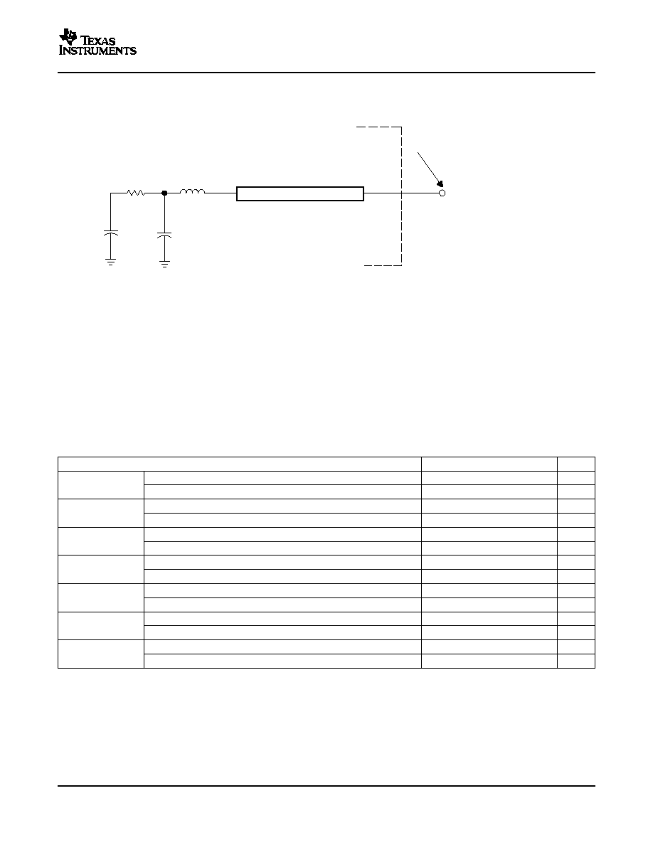
www.ti.com
6.5.2
Test Load Circuit
Transmission Line
4.0 pF
1.85 pF
Z0 = 50
()
Tester Pin Electronics
Data Sheet Timing Reference Point
Output
Under
Test
42
3.5 nH
Device Pin
(B)
6.5.3
Device Clock Table
TMS320F2809, TMS320F2808, TMS320F2806
TMS320F2802, TMS320F2801, UCD9501
TMS320C2802, TMS320C2801 Digital Signal Processors
SPRS230G ≠ OCTOBER 2003 ≠ REVISED FEBRUARY 2006
This test load circuit is used to measure all switching characteristics provided in this document.
A.
Input requirements in this data sheet are tested with an input slew rate of < 4 Volts per nanosecond (4 V/ns) at the
device pin.
B.
The data sheet provides timing at the device pin. For output timing analysis, the tester pin electronics and its
transmission line effects must be taken into account. A transmission line with a delay of 2 ns or longer can be used to
produce the desired transmission line effect. The transmission line is intended as a load only. It is not necessary to
add or subtract the transmission line delay (2 ns or longer) from the data sheet timing.
Figure 6-3. 3.3-V Test Load Circuit
This section provides the timing requirements and switching characteristics for the various clock options
available on the 280x DSPs.
Table 6-6
lists the cycle times of various clocks.
Table 6-6. TMS320x280x Clock Table and Nomenclature
MIN
NOM
MAX
UNIT
t
c(OSC)
, Cycle time
28.6
50
ns
On-chip oscillator
clock
Frequency
20
35
MHz
t
c(CI)
, Cycle time
10
250
ns
XCLKIN
(1)
Frequency
4
100
MHz
t
c(SCO)
, Cycle time
10
500
ns
SYSCLKOUT
Frequency
2
100
MHz
t
c(XCO)
, Cycle time
10
2000
ns
XCLKOUT
Frequency
0.5
100
MHz
t
c(HCO)
, Cycle time
10
20
(3)
ns
HSPCLK
(2)
Frequency
50
(3)
100
MHz
t
c(LCO)
, Cycle time
10
40
(3)
ns
LSPCLK
(2)
Frequency
25
(3)
100
MHz
t
c(ADCCLK)
, Cycle time
80
ns
ADC clock
Frequency
12.5
MHz
(1)
This also applies to the X1 pin if a 1.8-V oscillator is used.
(2)
Lower LSPCLK and HSPCLK will reduce device power consumption.
(3)
This is the default reset value if SYSCLKOUT = 100 MHz.
Electrical Specifications
97
www.ti.com
6.6
Clock Requirements and Characteristics
TMS320F2809, TMS320F2808, TMS320F2806
TMS320F2802, TMS320F2801, UCD9501
TMS320C2802, TMS320C2801 Digital Signal Processors
SPRS230G ≠ OCTOBER 2003 ≠ REVISED FEBRUARY 2006
Table 6-7. Input Clock Frequency
PARAMETER
MIN
TYP
MAX
UNIT
Resonator (X1/X2)
20
35
Crystal (X1/X2)
20
35
f
x
Input clock frequency
MHz
Without PLL
4
100
External oscillator/clock
source (XCLKIN or X1 pin)
With PLL
5
30
f
l
Limp mode SYSCLKOUT frequency range (with /2 enabled)
1-5
MHz
Table 6-8. XCLKIN
(1)
Timing Requirements - PLL Enabled
NO.
MIN
MAX
UNIT
C8
t
c(CI)
Cycle time, XCLKIN
33.3
200
ns
C9
t
f(CI)
Fall time, XCLKIN
6
ns
C10
t
r(CI)
Rise time, XCLKIN
6
ns
C11
t
w(CIL)
Pulse duration, XCLKIN low as a percentage of t
c(OSCCLK)
45
55
%
C12
t
w(CIH)
Pulse duration, XCLKIN high as a percentage of t
c(OSCCLK)
45
55
%
(1)
This applies to the X1 pin also.
Table 6-9. XCLKIN
(1)
Timing Requirements - PLL Disabled
NO.
MIN
MAX
UNIT
C8
t
c(CI)
Cycle time, XCLKIN
10
250
ns
C9
t
f(CI)
Fall time, XCLKIN
Up to 20 MHz
6
ns
20 MHz to 100 MHz
2
ns
C10
t
r(CI)
Rise time, XCLKIN
Up to 20 MHz
6
ns
20 MHz to 100 MHz
2
ns
C11
t
w(CIL)
Pulse duration, XCLKIN low as a percentage of t
c(OSCCLK)
45
55
%
C12
t
w(CIH)
Pulse duration, XCLKIN high as a percentage of t
c(OSCCLK)
45
55
%
(1)
This applies to the X1 pin also.
The possible configuration modes are shown in
Table 3-16
.
Table 6-10. XCLKOUT Switching Characteristics (PLL Bypassed or Enabled)
(1) (2)
NO.
PARAMETER
MIN
TYP
MAX
UNIT
C1
t
c(XCO)
Cycle time, XCLKOUT
10
ns
C3
t
f(XCO)
Fall time, XCLKOUT
2
ns
C4
t
r(XCO)
Rise time, XCLKOUT
2
ns
C5
t
w(XCOL)
Pulse duration, XCLKOUT low
H-2
H+2
ns
C6
t
w(XCOH)
Pulse duration, XCLKOUT high
H-2
H+2
ns
t
p
PLL lock time
131072t
c(OSCCLK)
(3)
cycles
(1)
A load of 40 pF is assumed for these parameters.
(2)
H = 0.5t
c(XCO)
(3)
OSCCLK is either the output of the on-chip oscillator or the output from an external oscillator.
Electrical Specifications
98
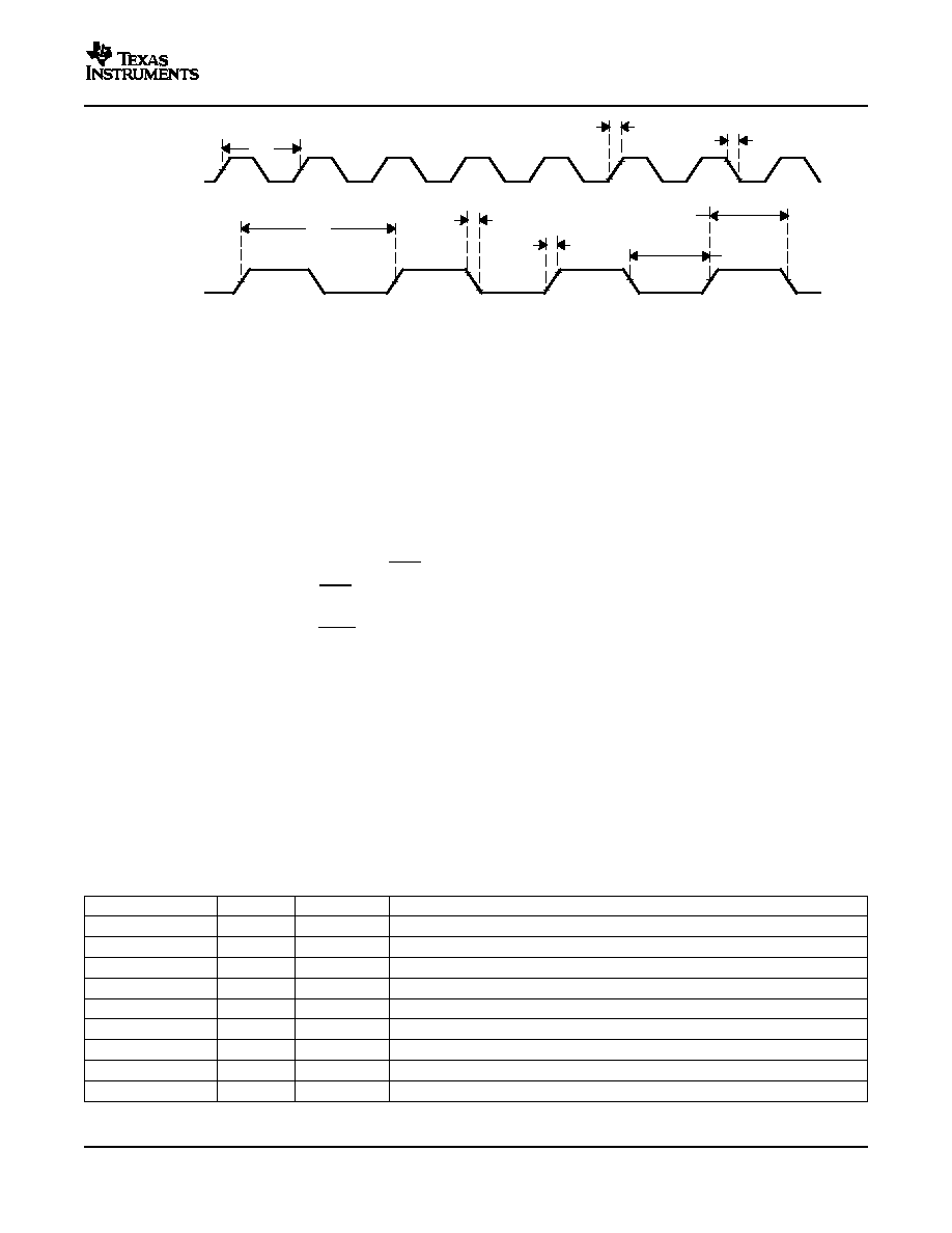
www.ti.com
C4
C3
XCLKOUT
(B)
XCLKIN
(A)
C5
C9
C10
C1
C8
C6
6.7
Power Sequencing
6.7.1
Power Management and Supervisory Circuit Solutions
TMS320F2809, TMS320F2808, TMS320F2806
TMS320F2802, TMS320F2801, UCD9501
TMS320C2802, TMS320C2801 Digital Signal Processors
SPRS230G ≠ OCTOBER 2003 ≠ REVISED FEBRUARY 2006
A.
The relationship of XCLKIN to XCLKOUT depends on the divide factor chosen. The waveform relationship shown is
intended to illustrate the timing parameters only and may differ based on actual configuration.
B.
XCLKOUT configured to reflect SYSCLKOUT.
Figure 6-4. Clock Timing
No requirements are placed on the power up/down sequence of the various power pins to ensure the
correct reset state for all the modules. However, if the 3.3-V transistors in the level shifting output buffers
of the I/O pins are powered prior to the 1.8-V transistors, it is possible for the output buffers to turn on,
causing a glitch to occur on the pin during power up. To avoid this behavior, power the V
DD
pins prior to or
simultaneously with the V
DDIO
pins, ensuring that the V
DD
pins have reached 0.7 V before the V
DDIO
pins
reach 0.7 V.
There are some requirements on the XRS pin:
1. During power up, the XRS pin must be held low for t
w(RSL1)
after the input clock is stable (see
Table 6-12
). This is to enable the entire device to start from a known condition.
2. During power down, the XRS pin must be pulled low at least 8
µ
s prior to V
DD
reaching 1.5 V. This is to
enhance flash reliability.
Additionally it is recommended that no voltage larger than a diode drop (0.7 V) should be applied to any
pin prior to powering up the device. Voltages applied to pins on an unpowered device can bias internal p-n
junctions in unintended ways and produce unpredictable results.
Table 6-11
lists the power management and supervisory circuit solutions for 280x DSPs. LDO selection
depends on the total power consumed in the end application. Go to www.power.ti.com for a complete list
of TI power ICs or select TI DSP Power Solutions for links to the DSP Power Selection Guide
(slub006a.pdf) and links to specific power reference designs.
Table 6-11. Power Management and Supervisory Circuit Solutions
SUPPLIER
TYPE
PART
DESCRIPTION
Texas Instruments
LDO
TPS767D301
Dual 1-A low-dropout regulator (LDO) with supply voltage supervisor (SVS)
Texas Instruments
LDO
TPS70202
Dual 500/250-mA LDO with SVS
Texas Instruments
LDO
TPS766xx
250-mA LDO with PG
Texas Instruments
SVS
TPS3808
Open Drain SVS with programmable delay
Texas Instruments
SVS
TPS3803
Low-cost Open-drain SVS with 5
µ
S delay
Texas Instruments
LDO
TPS799xx
200-mA LDO in WCSP package
Texas Instruments
LDO
TPS736xx
400-mA LDO with 40 mV of V
DO
Texas Instruments
DC/DC
TPS62110
High V
in
1.2-A dc/dc converter in 4x4 QFN package
Texas Instruments
DC/DC
TPS6230x
500-mA converter in WCSP package
Electrical Specifications
99
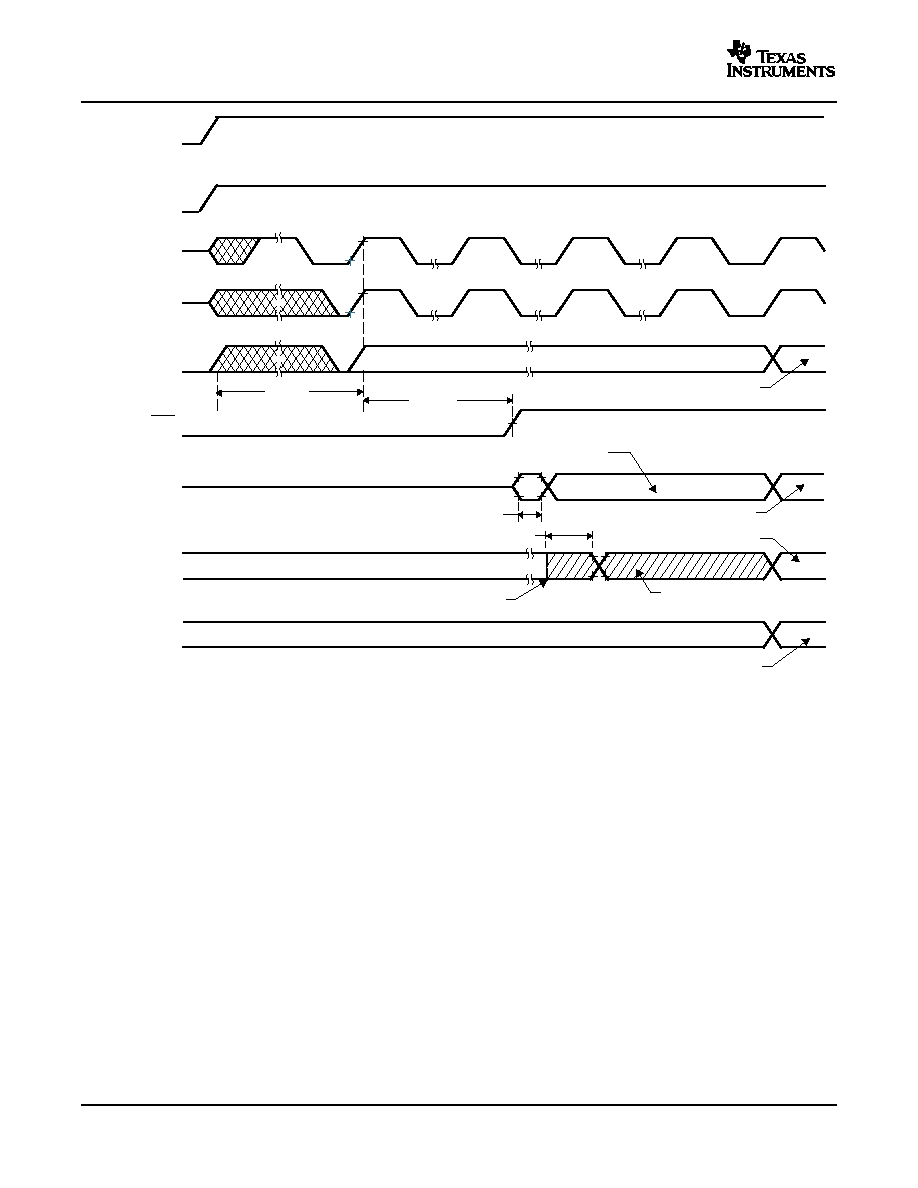
www.ti.com
t
w(RSL1)
t
h(boot-mode)
(B)
V
DDIO
, V
DD3VFL
V
DDA2
, V
DDAIO
(3.3 V)
XCLKIN
X1/X2
XRS
Boot-Mode
Pins
V
DD
, V
DD1A18,
V
DD2A18
(1.8 V)
XCLKOUT
I/O Pins
(C)
User-Code Dependent
User-Code Dependent
Boot-ROM Execution Starts
Peripheral/GPIO Function
Based on Boot Code
GPIO Pins as Input
OSCCLK/8
(A)
GPIO Pins as Input (State Depends on Internal PU/PD)
t
OSCST
User-Code Dependent
Address/Data/
Control
(Internal)
Address/Data Valid. Internal Boot-ROM Code Execution Phase
User-Code Execution Phase
t
d(EX)
TMS320F2809, TMS320F2808, TMS320F2806
TMS320F2802, TMS320F2801, UCD9501
TMS320C2802, TMS320C2801 Digital Signal Processors
SPRS230G ≠ OCTOBER 2003 ≠ REVISED FEBRUARY 2006
A.
Upon power up, SYSCLKOUT is OSCCLK/2. Since the XCLKOUTDIV bits in the XCLK register come up with a reset
state of 0, SYSCLKOUT is further divided by 4 before it appears at XCLKOUT. This explains why XCLKOUT =
OSCCLK/8 during this phase.
B.
After reset, the boot ROM code samples Boot Mode pins. Based on the status of the Boot Mode pin, the boot code
branches to destination memory or boot code function. If boot ROM code executes after power-on conditions (in
debugger environment), the boot code execution time is based on the current SYSCLKOUT speed. The SYSCLKOUT
will be based on user environment and could be with or without PLL enabled.
C.
See
Section 6.7
for requirements to ensure a high-impedance state for GPIO pins during power-up.
Figure 6-5. Power-on Reset
Electrical Specifications
100
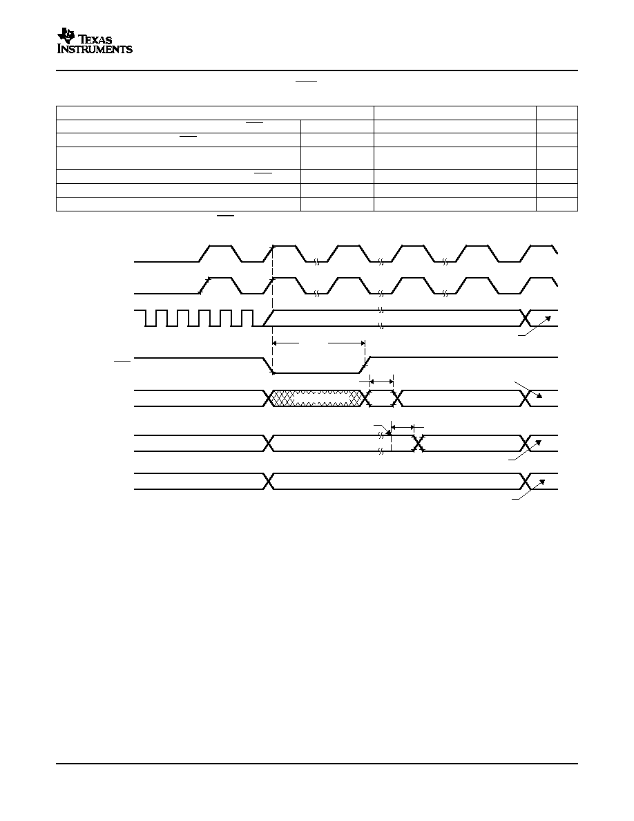
www.ti.com
t
h(boot-mode)
(A)
t
w(RSL2)
XCLKIN
X1/X2
XRS
Boot-Mode
Pins
XCLKOUT
I/O Pins
Address/Data/
Control
(Internal)
Boot-ROM Execution Starts
User-Code Execution Starts
User-Code Dependent
User-Code Execution Phase
(Don't Care)
User-Code Dependent
User-Code Execution
Peripheral/GPIO Function
User-Code Dependent
GPIO Pins as Input (State Depends on Internal PU/PD)
GPIO Pins as Input
Peripheral/GPIO Function
t
d(EX)
OSCCLK * 5
OSCCLK/8
TMS320F2809, TMS320F2808, TMS320F2806
TMS320F2802, TMS320F2801, UCD9501
TMS320C2802, TMS320C2801 Digital Signal Processors
SPRS230G ≠ OCTOBER 2003 ≠ REVISED FEBRUARY 2006
Table 6-12. Reset (XRS) Timing Requirements
MIN
NOM
MAX
UNIT
t
w(RSL1)
(1)
Pulse duration, stable XCLKIN to XRS high
8t
c(OSCCLK)
cycles
t
w(RSL2)
Pulse duration, XRS low
Warm reset
8t
c(OSCCLK)
cycles
Pulse duration, reset pulse generated by
t
w(WDRS)
512t
c(OSCCLK)
cycles
watchdog
t
d(EX)
Delay time, address/data valid after XRS high
32t
c(OSCCLK)
cycles
t
OSCST
(2)
Oscillator start-up time
1
10
ms
t
h(boot-mode)
Hold time for boot-mode pins
200t
c(OSCCLK)
cycles
(1)
In addition to the t
w(RSL1)
requirement, XRS has to be low at least for 1 ms after V
DD
reaches 1.5 V.
(2)
Dependent on crystal/resonator and board design.
A.
After reset, the Boot ROM code samples BOOT Mode pins. Based on the status of the Boot Mode pin, the boot code
branches to destination memory or boot code function. If Boot ROM code executes after power-on conditions (in
debugger environment), the Boot code execution time is based on the current SYSCLKOUT speed. The
SYSCLKOUT will be based on user environment and could be with or without PLL enabled.
Figure 6-6. Warm Reset
Figure 6-7
shows an example for the effect of writing into PLLCR register. In the first phase, PLLCR =
0x0004 and SYSCLKOUT = OSCCLK x 2. The PLLCR is then written with 0x0008. Right after the PLLCR
register is written, the PLL lock-up phase begins. During this phase, SYSCLKOUT = OSCCLK/2. After the
PLL lock-up is complete (which takes 131072 OSCCLK cycles), SYSCLKOUT reflects the new operating
frequency, OSCCLK x 4.
Electrical Specifications
101
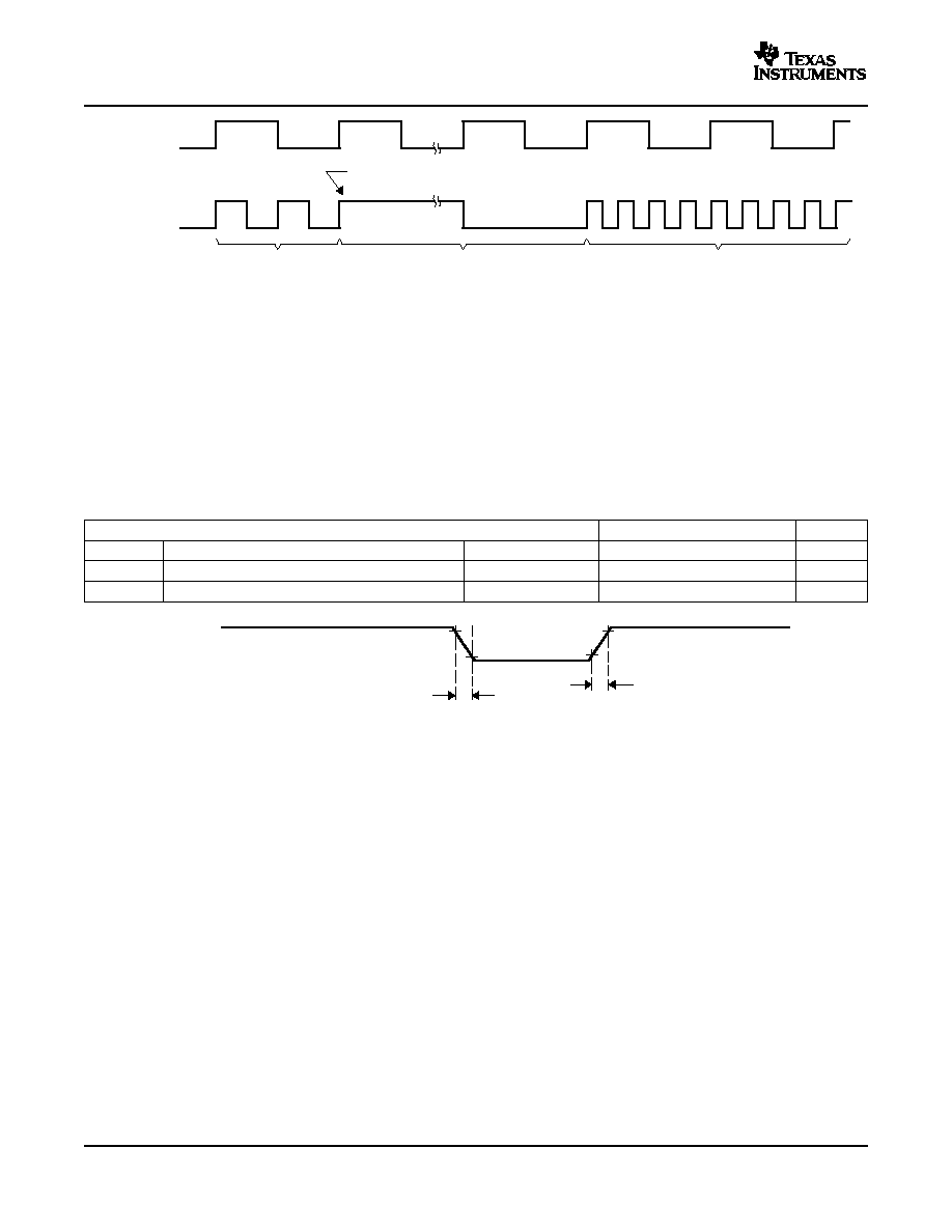
www.ti.com
OSCCLK
SYSCLKOUT
Write to PLLCR
OSCCLK * 2
(Current CPU
Frequency)
OSCCLK/2
(CPU Frequency While PLL is Stabilizing
With the Desired Frequency. This Period
(PLL Lock-up Time, t
p
) is
131072 OSCCLK Cycles Long.)
OSCCLK * 4
(Changed CPU Frequency)
6.8
General-Purpose Input/Output (GPIO)
6.8.1
GPIO - Output Timing
GPIO
t
r(GPO)
t
f(GPO)
TMS320F2809, TMS320F2808, TMS320F2806
TMS320F2802, TMS320F2801, UCD9501
TMS320C2802, TMS320C2801 Digital Signal Processors
SPRS230G ≠ OCTOBER 2003 ≠ REVISED FEBRUARY 2006
Figure 6-7. Example of Effect of Writing Into PLLCR Register
Table 6-13. General-Purpose Output Switching Characteristics
PARAMETER
MIN
MAX
UNIT
t
r(GPO)
Rise time, GPIO switching low to high
All GPIOs
8
ns
t
f(GPO)
Fall time, GPIO switching high to low
All GPIOs
8
ns
t
fGPO
Toggling frequency, GPO pins
25
MHz
Figure 6-8. General-Purpose Output Timing
Electrical Specifications
102
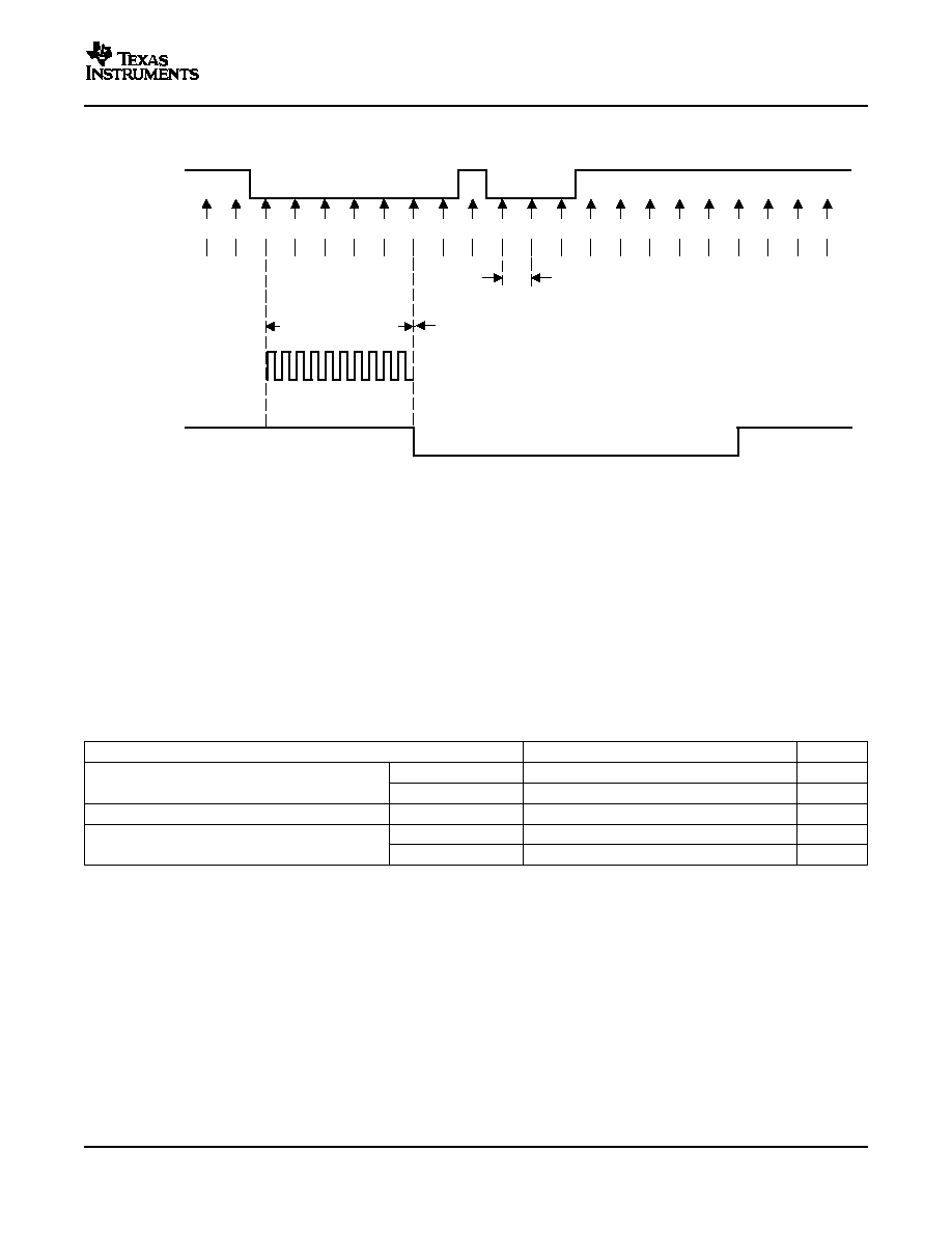
www.ti.com
6.8.2
GPIO - Input Timing
GPIO Signal
1
Sampling Window
Output From
Qualifier
1
1
1
1
1
1
1
1
1
1
1
0
0
0
0
0
0
0
0
0
0
SYSCLKOUT
QUALPRD = 1
(SYSCLKOUT/2)
(SYSCLKOUT cycle * 2 * QUALPRD) * 5
(C)
)
(A)
GPxQSELn = 1,0 (6 samples)
Sampling Period determined
by GPxCTRL[QUALPRD]
(B)
(D)
t
w(SP)
t
w(IQSW)
TMS320F2809, TMS320F2808, TMS320F2806
TMS320F2802, TMS320F2801, UCD9501
TMS320C2802, TMS320C2801 Digital Signal Processors
SPRS230G ≠ OCTOBER 2003 ≠ REVISED FEBRUARY 2006
A.
This glitch will be ignored by the input qualifier. The QUALPRD bit field specifies the qualification sampling period. It
can vary from 00 to 0xFF. If QUALPRD = 00, then the sampling period is 1 SYSCLKOUT cycle. For any other value
"n", the qualification sampling period in 2n SYSCLKOUT cycles (i.e., at every 2n SYSCLKOUT cycles, the GPIO pin
will be sampled).
B.
The qualification period selected via the GPxCTRL register applies to groups of 8 GPIO pins.
C.
The qualification block can take either three or six samples. The GPxQSELn Register selects which sample mode is
used.
D.
In the example shown, for the qualifier to detect the change, the input should be stable for 10 SYSCLKOUT cycles or
greater. In other words, the inputs should be stable for (5 x QUALPRD x 2) SYSCLKOUT cycles. This would ensure
5 sampling periods for detection to occur. Since external signals are driven asynchronously, an 13-SYSCLKOUT-wide
pulse ensures reliable recognition.
Figure 6-9. Sampling Mode
Table 6-14. General-Purpose Input Timing Requirements
MIN
MAX
UNIT
QUALPRD = 0
1t
c(SCO)
cycles
t
w(SP)
Sampling period
QUALPRD
0
2t
c(SCO)
* QUALPRD
cycles
t
w(IQSW)
Input qualifier sampling window
t
w(SP)
* (n
(1)
- 1)
cycles
Synchronous mode
2t
c(SCO)
cycles
t
w(GPI)
(2)
Pulse duration, GPIO low/high
With input qualifier
t
w(IQSW)
+ t
w(SP)
+ 1t
c(SCO)
cycles
(1)
"n" represents the number of qualification samples as defined by GPxQSELn register.
(2)
For t
w(GPI)
, pulse width is measured from V
IL
to V
IL
for an active low signal and V
IH
to V
IH
for an active high signal.
Electrical Specifications
103
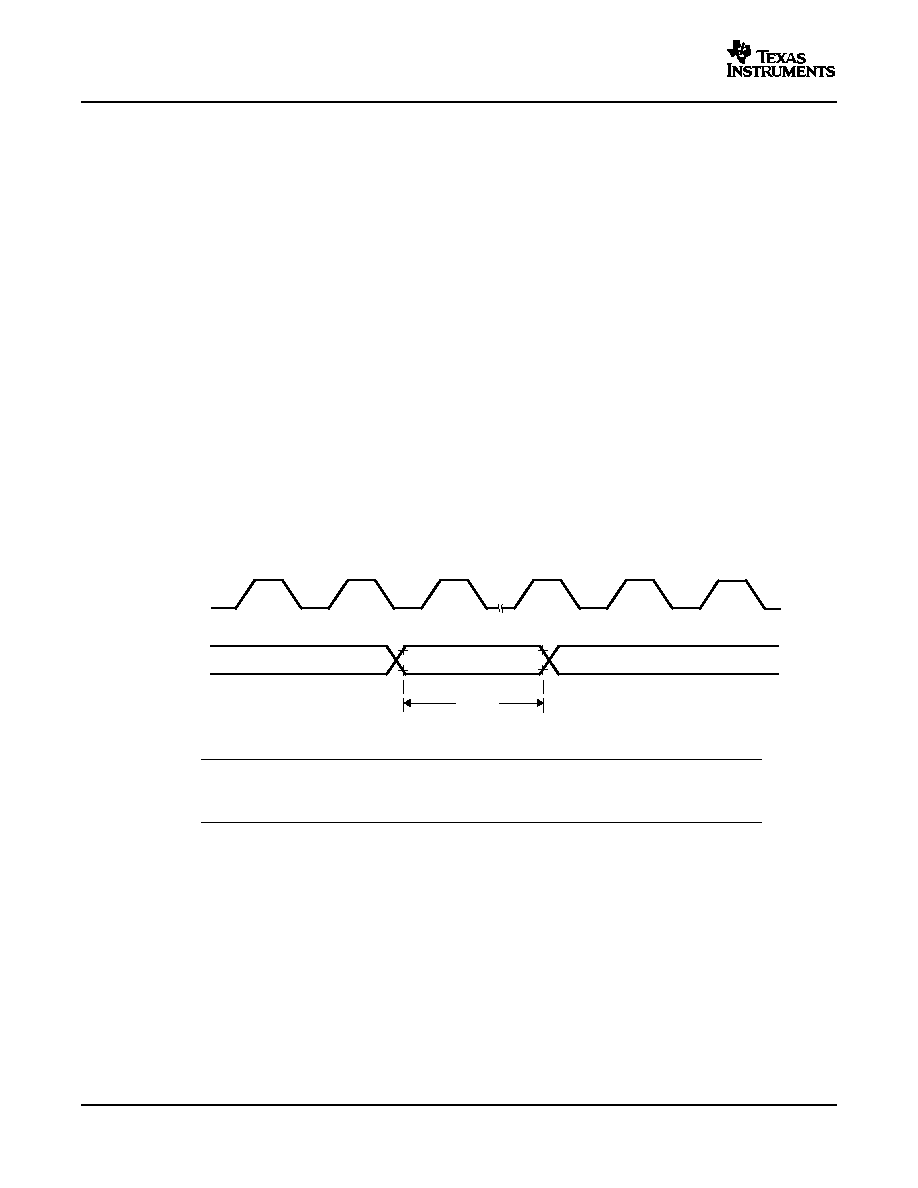
www.ti.com
GPIOxn
XCLKOUT
t
w(GPI)
TMS320F2809, TMS320F2808, TMS320F2806
TMS320F2802, TMS320F2801, UCD9501
TMS320C2802, TMS320C2801 Digital Signal Processors
SPRS230G ≠ OCTOBER 2003 ≠ REVISED FEBRUARY 2006
6.8.3
Sampling Window Width for Input Signals
The following section summarizes the sampling window width for input signals for various input qualifier
configurations.
Sampling frequency denotes how often a signal is sampled with respect to SYSCLKOUT.
Sampling frequency = SYSCLKOUT/(2 * QUALPRD), if QUALPRD
0
Sampling frequency = SYSCLKOUT, if QUALPRD = 0
Sampling period = SYSCLKOUT cycle x 2 x QUALPRD, if QUALPRD
0
In the above equations, SYSCLKOUT cycle indicates the time period of SYSCLKOUT.
Sampling period = SYSCLKOUT cycle, if QUALPRD = 0
In a given sampling window, either 3 or 6 samples of the input signal are taken to determine the validity of
the signal. This is determined by the value written to GPxQSELn register.
Case 1:
Qualification using 3 samples
Sampling window width = (SYSCLKOUT cycle x 2 x QUALPRD) x 2, if QUALPRD
0
Sampling window width = (SYSCLKOUT cycle) x 2, if QUALPRD = 0
Case 2:
Qualification using 6 samples
Sampling window width = (SYSCLKOUT cycle x 2 x QUALPRD) x 5, if QUALPRD
0
Sampling window width = (SYSCLKOUT cycle) x 5, if QUALPRD = 0
Figure 6-10. General-Purpose Input Timing
NOTE
The
pulse-width
requirement
for
general-purpose
input
is
applicable
for
the
XINT2_ADCSOC signal as well.
Electrical Specifications
104
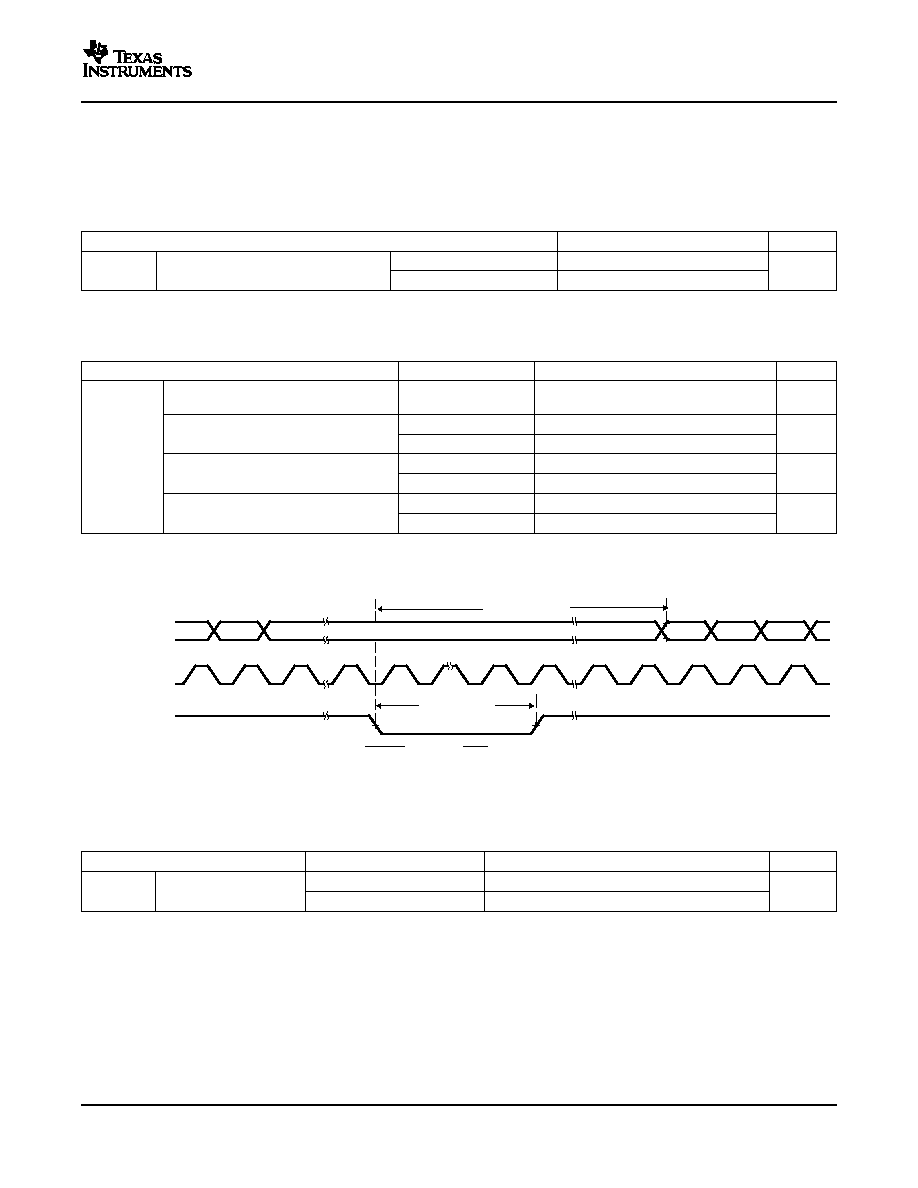
www.ti.com
WAKE INT
(A)
XCLKOUT
Address/Data
(internal)
t
d(WAKE-IDLE)
t
w(WAKE-INT)
TMS320F2809, TMS320F2808, TMS320F2806
TMS320F2802, TMS320F2801, UCD9501
TMS320C2802, TMS320C2801 Digital Signal Processors
SPRS230G ≠ OCTOBER 2003 ≠ REVISED FEBRUARY 2006
6.8.4
Low-Power Mode Wakeup Timing
Table 6-15
shows the timing requirements,
Table 6-16
shows the switching characteristics, and
Figure 6-11
shows the timing diagram for IDLE mode.
Table 6-15. IDLE Mode Timing Requirements
(1)
MIN
NOM
MAX
UNIT
Without input qualifier
2t
c(SCO)
t
w(WAKE-INT)
Pulse duration, external wake-up signal
cycles
With input qualifier
5t
c(SCO)
+ t
w(IQSW)
(1)
For an explanation of the input qualifier parameters, see
Table 6-14
.
Table 6-16. IDLE Mode Switching Characteristics
(1)
PARAMETER
TEST CONDITIONS
MIN
TYP
MAX
UNIT
Delay time, external wake signal to
program execution resume
(2)
Without input qualifier
20t
c(SCO)
cycles
∑
Wake-up from Flash
≠
Flash module in active state
With input qualifier
20t
c(SCO)
+ t
w(IQSW)
t
d(WAKE-IDLE)
Without input qualifier
1050t
c(SCO)
cycles
∑
Wake-up from Flash
≠
Flash module in sleep state
With input qualifier
1050t
c(SCO)
+ t
w(IQSW)
Without input qualifier
20t
c(SCO)
cycles
∑
Wake-up from SARAM
With input qualifier
20t
c(SCO)
+ t
w(IQSW)
(1)
For an explanation of the input qualifier parameters, see
Table 6-14
.
(2)
This is the time taken to begin execution of the instruction that immediately follows the IDLE instruction. execution of an ISR (triggered
by the wake up) signal involves additional latency.
A.
WAKE INT can be any enabled interrupt, WDINT, XNMI, or XRS.
Figure 6-11. IDLE Entry and Exit Timing
Table 6-17. STANDBY Mode Timing Requirements
TEST CONDITIONS
MIN
NOM
MAX
UNIT
Without input qualification
3t
c(OSCCLK)
Pulse duration, external
t
w(WAKE-INT)
cycles
wake-up signal
With input qualification
(1)
(2 + QUALSTDBY) * t
c(OSCCLK)
(1)
QUALSTDBY is a 6-bit field in the LPMCR0 register.
Electrical Specifications
105
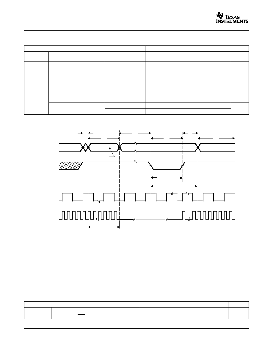
www.ti.com
t
w(WAKE-INT)
t
d(WAKE-STBY)
t
d(IDLE-XCOL)
Wake-up
Signal
X1/X2 or
X1 or
XCLKIN
XCLKOUT
STANDBY
Normal Execution
STANDBY
Flushing Pipeline
(A)
(B)
(C)
(D)
(E)
(F)
Device
Status
TMS320F2809, TMS320F2808, TMS320F2806
TMS320F2802, TMS320F2801, UCD9501
TMS320C2802, TMS320C2801 Digital Signal Processors
SPRS230G ≠ OCTOBER 2003 ≠ REVISED FEBRUARY 2006
Table 6-18. STANDBY Mode Switching Characteristics
PARAMETER
TEST CONDITIONS
MIN
TYP
MAX
UNIT
Delay time, IDLE instruction
t
d(IDLE-XCOL)
32t
c(SCO)
45t
c(SCO)
cycles
executed to XCLKOUT low
Delay time, external wake signal
cycles
to program execution resume
(1)
Without input qualifier
100t
c(SCO)
∑
Wake up from flash
cycles
≠
Flash module in active
With input qualifier
100t
c(SCO)
+ t
w(WAKE-INT)
state
t
d(WAKE-STBY)
Without input qualifier
1125t
c(SCO)
∑
Wake up from flash
cycles
≠
Flash module in sleep
With input qualifier
1125t
c(SCO)
+ t
w(WAKE-INT)
state
Without input qualifier
100t
c(SCO)
cycles
∑
Wake up from SARAM
With input qualifier
100t
c(SCO)
+ t
w(WAKE-INT)
(1)
This is the time taken to begin execution of the instruction that immediately follows the IDLE instruction. execution of an ISR (triggered
by the wake up signal) involves additional latency.
A.
IDLE instruction is executed to put the device into STANDBY mode.
B.
The PLL block responds to the STANDBY signal. SYSCLKOUT is held for approximately 32 cycles before being
turned off. This 32-cycle delay enables the CPU pipe and any other pending operations to flush properly.
C.
Clock to the peripherals are turned off. However, the PLL and watchdog are not shut down. The device is now in
STANDBY mode.
D.
The external wake-up signal is driven active.
E.
After a latency period, the STANDBY mode is exited.
F.
Normal execution resumes. The device will respond to the interrupt (if enabled).
Figure 6-12. STANDBY Entry and Exit Timing Diagram
Table 6-19. HALT Mode Timing Requirements
MIN
NOM
MAX
UNIT
t
w(WAKE-GPIO)
Pulse duration, GPIO wake-up signal
t
oscst
+ 2t
c(OSCCLK)
(1)
cycles
t
w(WAKE-XRS)
Pulse duration, XRS wakeup signal
t
oscst
+ 8t
c(OSCCLK)
cycles
(1)
See
Table 6-12
for an explanation of t
oscst
.
Electrical Specifications
106
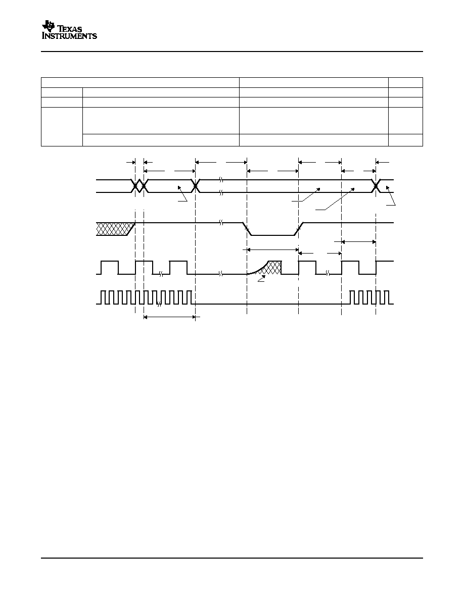
www.ti.com
t
d(IDLE-XCOL)
X1/X2
or XCLKIN
XCLKOUT
HALT
HALT
Wake-up Latency
Flushing Pipeline
t
d(WAKE-HALT)
(A)
(B)
(C)
(D)
Device
Status
(E)
(G)
(F)
PLL Lock-up Time
Normal
Execution
t
w(WAKE-GPIO)
t
p
GPIOn
Oscillator Start-up Time
TMS320F2809, TMS320F2808, TMS320F2806
TMS320F2802, TMS320F2801, UCD9501
TMS320C2802, TMS320C2801 Digital Signal Processors
SPRS230G ≠ OCTOBER 2003 ≠ REVISED FEBRUARY 2006
Table 6-20. HALT Mode Switching Characteristics
PARAMETER
MIN
TYP
MAX
UNIT
t
d(IDLE-XCOL)
Delay time, IDLE instruction executed to XCLKOUT low
32t
c(SCO)
45t
c(SCO)
cycles
t
p
PLL lock-up time
131072t
c(OSCCLK)
cycles
Delay time, PLL lock to program execution resume
1125t
c(SCO)
cycles
∑
Wake up from flash
t
d(WAKE-HALT)
≠
Flash module in sleep state
35t
c(SCO)
cycles
∑
Wake up from SARAM
A.
IDLE instruction is executed to put the device into HALT mode.
B.
The PLL block responds to the HALT signal. SYSCLKOUT is held for approximately 32 cycles before the oscillator is
turned off and the CLKIN to the core is stopped. This 32-cycle delay enables the CPU pipe and any other pending
operations to flush properly.
C.
Clocks to the peripherals are turned off and the PLL is shut down. If a quartz crystal or ceramic resonator is used as
the clock source, the internal oscillator is shut down as well. The device is now in HALT mode and consumes
absolute minimum power.
D.
When the GPIOn pin is driven low, the oscillator is turned on and the oscillator wake-up sequence is initiated. The
GPIO pin should be driven high only after the oscillator has stabilized. This enables the provision of a clean clock
signal during the PLL lock sequence. Since the falling edge of the GPIO pin asynchronously begins the wakeup
procedure, care should be taken to maintain a low noise environment prior to entering and during HALT mode.
E.
When GPIOn is deactivated, it initiates the PLL lock sequence, which takes 131,072 OSCCLK (X1/X2 or X1 or
XCLKIN) cycles.
F.
When CLKIN to the core is enabled, the device will respond to the interrupt (if enabled), after a latency. The HALT
mode is now exited.
G.
Normal operation resumes.
Figure 6-13. HALT Wake-Up Using GPIOn
Electrical Specifications
107
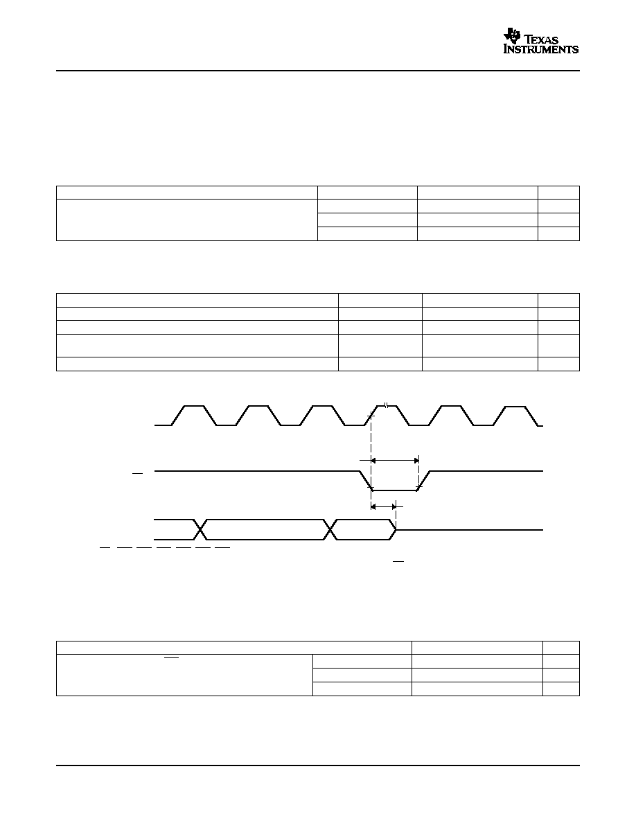
www.ti.com
6.9
Enhanced Control Peripherals
6.9.1
Enhanced Pulse Width Modulator (ePWM) Timing
PWM
(B)
TZ
XCLKOUT
(A)
t
w(TZ)
t
d(TZ-PWM)HZ
TMS320F2809, TMS320F2808, TMS320F2806
TMS320F2802, TMS320F2801, UCD9501
TMS320C2802, TMS320C2801 Digital Signal Processors
SPRS230G ≠ OCTOBER 2003 ≠ REVISED FEBRUARY 2006
PWM refers to PWM outputs on ePWM1-6.
Table 6-21
shows the PWM timing requirements and
Table 6-22
, switching characteristics.
Table 6-21. ePWM Timing Requirements
(1)
TEST CONDITIONS
MIN
MAX
UNIT
t
w(SYCIN)
Sync input pulse width
Asynchronous
2t
c(SCO)
cycles
Synchronous
2t
c(SCO)
cycles
With input qualifier
1t
c(SCO)
+ t
w(IQSW)
cycles
(1)
For an explanation of the input qualifier parameters, see
Table 6-14
.
Table 6-22. ePWM Switching Characteristics
PARAMETER
TEST CONDITIONS
MIN
MAX
UNIT
t
w(PWM)
Pulse duration, PWMx output high/low
20
ns
t
w(SYNCOUT)
Sync output pulse width
8t
c(SCO)
cycles
t
d(PWM)tza
Delay time, trip input active to PWM forced high
no pin load
25
ns
Delay time, trip input active to PWM forced low
t
d(TZ-PWM)HZ
Delay time, trip input active to PWM Hi-Z
20
ns
6.9.2
Trip-Zone Input Timing
A.
TZ - TZ1, TZ2, TZ3, TZ4, TZ5, TZ6
B.
PWM refers to all the PWM pins in the device. The state of the PWM pins after TZ is taken high depends on the PWM
recovery software.
Figure 6-14. PWM Hi-Z Characteristics
Table 6-23. Trip-Zone input Timing Requirements
(1)
MIN
MAX
UNIT
t
w(TZ)
Pulse duration, TZx input low
Asynchronous
1t
c(SCO)
cycles
Synchronous
2t
c(SCO)
cycles
With input qualifier
1t
c(SCO)
+ t
w(IQSW)
cycles
(1)
For an explanation of the input qualifier parameters, see
Table 6-14
.
Electrical Specifications
108
www.ti.com
TMS320F2809, TMS320F2808, TMS320F2806
TMS320F2802, TMS320F2801, UCD9501
TMS320C2802, TMS320C2801 Digital Signal Processors
SPRS230G ≠ OCTOBER 2003 ≠ REVISED FEBRUARY 2006
Table 6-24
shows the high-resolution PWM switching characteristics.
Table 6-24. High Resolution PWM Characteristics at SYSCLKOUT = (60 - 100 MHz)
MIN
TYP
MAX
UNIT
Micro Edge Positioning (MEP) step size
(1)
150
310
ps
(1)
Maximum MEP step size is based on worst-case process, maximum temperature and maximum voltage. MEP step size will increase
with low voltage and high temperature and decrease with voltage and cold temperature.
Applications that use the HRPWM feature should use MEP Scale Factor Optimizer (SFO) estimation software functions. See the TI
software libraries for details of using SFO function in end applications. SFO functions help to estimate the number of MEP steps per
SYSCLKOUT period dynamically while the HRPWM is in operation.
Table 6-25
shows the eCAP timing requirement and
Table 6-26
shows the eCAP switching characteristics.
Table 6-25. Enhanced Capture (eCAP) Timing Requirement
(1)
TEST CONDITIONS
MIN
MAX
UNIT
t
w(CAP)
Capture input pulse width
Asynchronous
2t
c(SCO)
cycles
Synchronous
2t
c(SCO)
cycles
With input qualifier
1t
c(SCO)
+ t
w(IQSW)
cycles
(1)
For an explanation of the input qualifier parameters, see
Table 6-14
.
Table 6-26. eCAP Switching Characteristics
PARAMETER
TEST CONDITIONS
MIN
MAX
UNIT
t
w(APWM)
Pulse duration, APWMx output high/low
20
ns
Table 6-27
shows the eQEP timing requirement and
Table 6-28
shows the eQEP switching
characteristics.
Table 6-27. Enhanced Quadrature Encoder Pulse (eQEP) Timing Requirements
(1)
TEST CONDITIONS
MIN
MAX
UNIT
t
w(QEPP)
QEP input period
Asynchronous/synchronous
2t
c(SCO)
cycles
With input qualifier
2(1t
c(SCO)
+ t
w(IQSW)
)
cycles
t
w(INDEXH)
QEP Index Input High time
Asynchronous/synchronous
2t
c(SCO)
cycles
With input qualifier
2t
c(SCO)
+t
w(IQSW)
cycles
t
w(INDEXL)
QEP Index Input Low time
Asynchronous/synchronous
2t
c(SCO)
cycles
With input qualifier
2t
c(SCO)
+ t
w(IQSW)
cycles
t
w(STROBH)
QEP Strobe High time
Asynchronous/synchronous
2t
c(SCO)
cycles
With input qualifier
2t
c(SCO)
+ t
w(IQSW)
cycles
t
w(STROBL)
QEP Strobe Input Low time
Asynchronous/synchronous
2t
c(SCO)
cycles
With input qualifier
2t
c(SCO)
+t
w(IQSW)
cycles
(1)
For an explanation of the input qualifier parameters, see
Table 6-14
.
Table 6-28. eQEP Switching Characteristics
PARAMETER
TEST CONDITIONS
MIN
MAX
UNIT
t
d(CNTR)xin
Delay time, external clock to counter increment
4t
c(SCO)
cycles
t
d(PXCSOUT)QEP
Delay time, QEP input edge to position compare sync output
6t
c(SCO)
cycles
Electrical Specifications
109
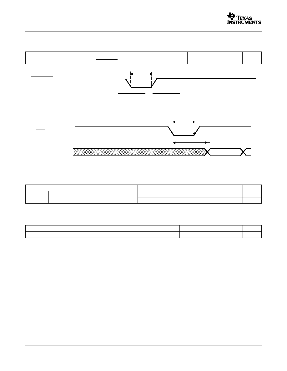
www.ti.com
ADCSOCAO
or
ADCSOCBO
t
w(ADCSOCAL)
6.9.3
External Interrupt Timing
XNMI, XINT1, XINT2
t
w(INT)
Interrupt Vector
t
d(INT)
Address bus
(internal)
TMS320F2809, TMS320F2808, TMS320F2806
TMS320F2802, TMS320F2801, UCD9501
TMS320C2802, TMS320C2801 Digital Signal Processors
SPRS230G ≠ OCTOBER 2003 ≠ REVISED FEBRUARY 2006
Table 6-29. External ADC Start-of-Conversion Switching Characteristics
PARAMETER
MIN
MAX
UNIT
t
w(ADCSOCAL)
Pulse duration, ADCSOCAO low
32t
c(HCO)
cycles
Figure 6-15. ADCSOCAO or ADCSOCBO Timing
Figure 6-16. External Interrupt Timing
Table 6-30. External Interrupt Timing Requirements
(1)
TEST CONDITIONS
MIN
MAX
UNIT
t
w(INT)
Pulse duration, INT input low/high
Synchronous
1t
c(SCO)
cycles
With qualifier
1t
c(SCO)
+ t
w(IQSW)
cycles
(1)
For an explanation of the input qualifier parameters, see
Table 6-14
.
Table 6-31. External Interrupt Switching Characteristics
(1)
PARAMETER
MIN
MAX
UNIT
t
d(INT)
Delay time, INT low/high to interrupt-vector fetch
t
w(IQSW)
+ 12t
c(SCO)
cycles
(1)
For an explanation of the input qualifier parameters, see
Table 6-14
.
Electrical Specifications
110
www.ti.com
6.9.4
I
2
C Electrical Specification and Timing
6.9.5
Serial Peripheral Interface (SPI) Master Mode Timing
TMS320F2809, TMS320F2808, TMS320F2806
TMS320F2802, TMS320F2801, UCD9501
TMS320C2802, TMS320C2801 Digital Signal Processors
SPRS230G ≠ OCTOBER 2003 ≠ REVISED FEBRUARY 2006
Table 6-32. I
2
C Timing
TEST CONDITIONS
MIN
MAX
UNIT
f
SCL
SCL clock frequency
I
2
C clock module frequency is between
400
kHz
7 MHz and 12 MHz and I
2
C prescaler and
clock divider registers are configured
appropriately
v
il
Low level input voltage
0.3 V
DDIO
V
V
ih
High level input voltage
0.7 V
DDIO
V
V
hys
Input hysteresis
0.05 V
DDIO
V
V
ol
Low level output voltage
3 mA sink current
0
0.4
V
t
LOW
Low period of SCL clock
I
2
C clock module frequency is between
1.3
µ
s
7 MHz and 12 MHz and I
2
C prescaler and
clock divider registers are configured
appropriately
t
HIGH
High period of SCL clock
I
2
C clock module frequency is between
0.6
µ
s
7 MHz and 12 MHz and I
2
C prescaler and
clock divider registers are configured
appropriately
l
I
Input current with an input voltage
-10
10
µ
A
between 0.1 V
DDIO
and 0.9 V
DDIO
MAX
Table 6-33
lists the master mode timing (clock phase = 0) and
Table 6-34
lists the timing (clock
phase = 1).
Figure 6-17
and
Figure 6-18
show the timing waveforms.
Electrical Specifications
111

www.ti.com
TMS320F2809, TMS320F2808, TMS320F2806
TMS320F2802, TMS320F2801, UCD9501
TMS320C2802, TMS320C2801 Digital Signal Processors
SPRS230G ≠ OCTOBER 2003 ≠ REVISED FEBRUARY 2006
Table 6-33. SPI Master Mode External Timing (Clock Phase = 0)
(1) (2) (3) (4) (5)
NO.
SPI WHEN (SPIBRR + 1) IS EVEN OR
SPI WHEN (SPIBRR + 1) IS ODD
UNIT
SPIBRR = 0 OR 2
AND SPIBRR > 3
MIN
MAX
MIN
MAX
1
t
c(SPC)M
Cycle time, SPICLK
4t
c(LCO)
128t
c(LCO)
5t
c(LCO)
127t
c(LCO)
ns
2
t
w(SPCH)M
Pulse duration, SPICLK high
0.5t
c(SPC)M
-10
0.5t
c(SPC)M
0.5t
c(SPC)M
- 0.5t
c(LCO)
- 10
0.5t
c(SPC)
M - 0.5t
c(LCO)
ns
(clock polarity = 0)
t
w(SPCL)M
Pulse duration, SPICLK low
0.5t
c(SPC)M
- 10
0.5t
c(SPC)M
0.5t
c(SPC)M
- 0.5t
c(LCO)
- 10
0.5t
c(SPC)M
- 0.5t
c(LCO)
(clock polarity = 1)
3
t
w(SPCL)M
Pulse duration, SPICLK low
0.5t
c(SPC)M
- 10
0.5
tc(SPC)M
0.5t
c(SPC)M
+ 0.5t
c(LCO)
-10
0.5t
c(SPC)M
+ 0.5t
c(LCO)
ns
(clock polarity = 0)
t
w(SPCH)M
Pulse duration, SPICLK high
0.5
tc(SPC)M
- 10
0.5t
c(SPC)M
0.5t
c(SPC)M
+ 0.5t
c(LCO)
- 10
0.5t
c(SPC)M
+ 0.5t
c(LCO)
(clock polarity = 1)
4
t
d(SPCH-SIMO)M
Delay time, SPICLK high to SPISIMO
10
10
ns
valid (clock polarity = 0)
t
d(SPCL-SIMO)M
Delay time, SPICLK low to SPISIMO
10
10
valid (clock polarity = 1)
5
t
v(SPCL-SIMO)M
Valid time, SPISIMO data valid after
0.5t
c(SPC)M
-10
0.5t
c(SPC)M
+ 0.5t
c(LCO)
-10
SPICLK low (clock polarity = 0)
t
v(SPCH-SIMO)M
Valid time, SPISIMO data valid after
0.5t
c(SPC)M
-10
0.5t
c(SPC)M
+ 0.5t
c(LCO)
-10
SPICLK high (clock polarity = 1)
8
t
su(SOMI-SPCL)M
Setup time, SPISOMI before SPICLK
35
35
ns
low (clock polarity = 0)
t
su(SOMI-SPCH)M
Setup time, SPISOMI before SPICLK
35
35
ns
high (clock polarity = 1)
9
t
v(SPCL-SOMI)M
Valid time, SPISOMI data valid after
0.25t
c(SPC)M
-10
0.5t
c(SPC)M
- 0.5t
c(LCO)
- 10
SPICLK low (clock polarity = 0)
t
v(SPCH-SOMI)M
Valid time, SPISOMI data valid after
0.25t
c(SPC)M
- 10
0.5t
c(SPC)M
- 0.5t
c(LCO)
- 10
ns
SPICLK high (clock polarity = 1)
(1)
The MASTER / SLAVE bit (SPICTL.2) is set and the CLOCK PHASE bit (SPICTL.3) is cleared.
(2)
t
c(SPC)
= SPI clock cycle time = LSPCLK/4 or LSPCLK/(SPIBRR +1)
(3)
t
c(LCO)
= LSPCLK cycle time
(4)
Internal clock prescalers must be adjusted such that the SPI clock speed is limited to the following SPI clock rate:
Master mode transmit 25-MHz MAX, master mode receive 12.5-MHz MAX
Slave mode transmit 12.5-MAX, slave mode receive 12.5-MHz MAX.
(5)
The active edge of the SPICLK signal referenced is controlled by the clock polarity bit (SPICCR.6).
112
Electrical Specifications
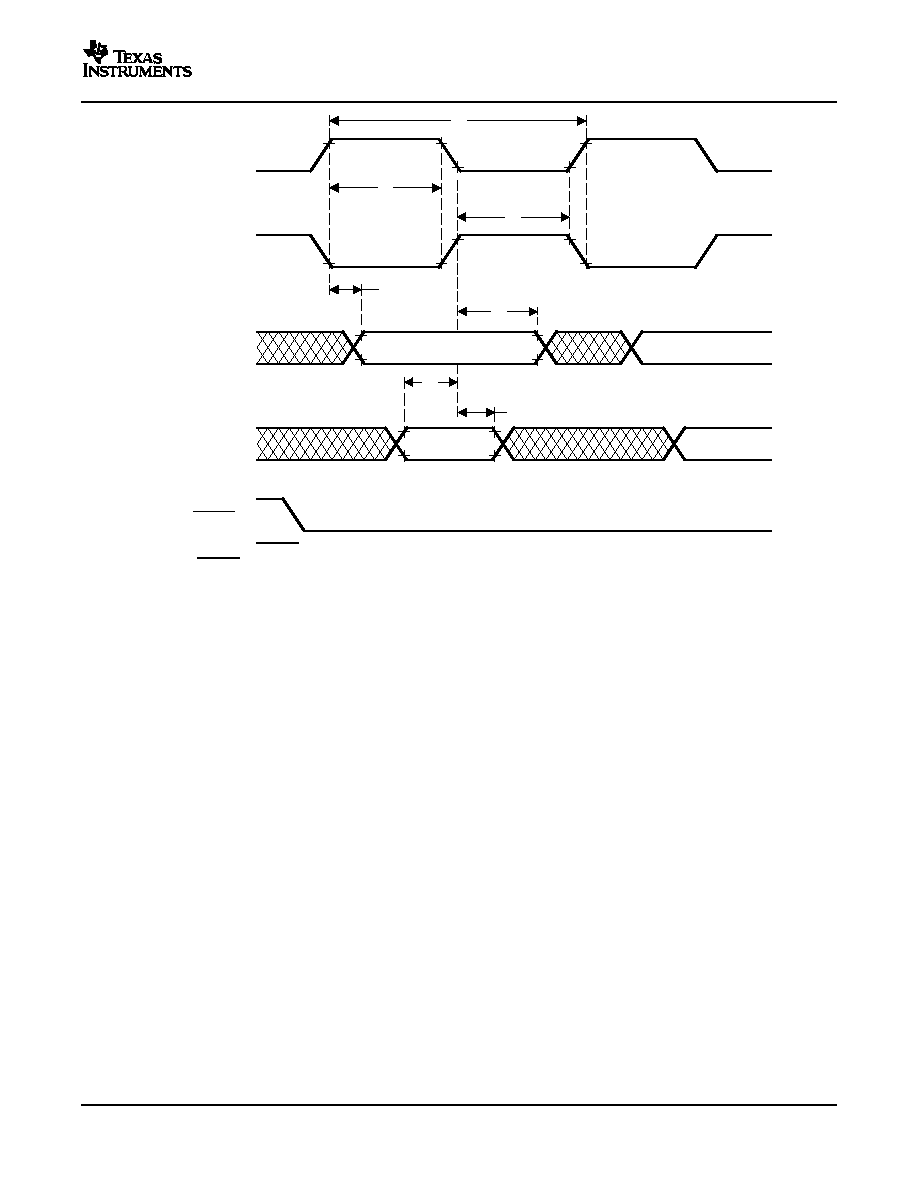
www.ti.com
9
4
SPISOMI
SPISIMO
SPICLK
(clock polarity = 1)
SPICLK
(clock polarity = 0)
Master In Data
Must Be Valid
Master Out Data Is Valid
8
5
3
2
1
SPISTE
(A)
TMS320F2809, TMS320F2808, TMS320F2806
TMS320F2802, TMS320F2801, UCD9501
TMS320C2802, TMS320C2801 Digital Signal Processors
SPRS230G ≠ OCTOBER 2003 ≠ REVISED FEBRUARY 2006
A.
In the master mode, SPISTE goes active 0.5t
c(SPC)
(minimum) before valid SPI clock edge. On the trailing end of the
word, the SPISTE will go inactive 0.5t
c(SPC)
after the receiving edge (SPICLK) of the last data bit.
Figure 6-17. SPI Master Mode External Timing (Clock Phase = 0)
Electrical Specifications
113

www.ti.com
TMS320F2809, TMS320F2808, TMS320F2806
TMS320F2802, TMS320F2801, UCD9501
TMS320C2802, TMS320C2801 Digital Signal Processors
SPRS230G ≠ OCTOBER 2003 ≠ REVISED FEBRUARY 2006
Table 6-34. SPI Master Mode External Timing (Clock Phase = 1)
(1) (2) (3) (4) (5)
NO.
SPI WHEN (SPIBRR + 1) IS EVEN
SPI WHEN (SPIBRR + 1) IS ODD
UNIT
OR SPIBRR = 0 OR 2
AND SPIBRR > 3
MIN
MAX
MIN
MAX
1
t
c(SPC)M
Cycle time, SPICLK
4t
c(LCO)
128t
c(LCO)
5t
c(LCO)
127t
c(LCO)
ns
2
t
w(SPCH)M
Pulse duration, SPICLK high (clock
0.5t
c(SPC)M
-10
0.5t
c(SPC)M
0.5t
c(SPC)M
- 0.5t
c (LCO)
-10
0.5t
c(SPC)M
- 0.5t
c(LCO)
ns
polarity = 0)
t
w(SPCL))M
Pulse duration, SPICLK low (clock
0.5t
c(SPC)M
-10
0.5t
c(SPC)M
0.5t
c(SPC)M
- 0.5t
c (LCO)
-10
0.5t
c(SPC)M
- 0.5t
c(LCO
ns
polarity = 1)
3
t
w(SPCL)M
Pulse duration, SPICLK low (clock
0.5t
c(SPC)M
-10
0.5t
c(SPC)M
0.5t
c(SPC)M
+ 0.5t
c(LCO)
- 10
0.5t
c(SPC)M
+ 0.5t
c(LCO)
ns
polarity = 0)
t
w(SPCH)M
Pulse duration, SPICLK high (clock
0.5t
c(SPC)M
-10
0.5t
c(SPC)M
0.5
tc(SPC)M
+ 0.5t
c(LCO)
-10
0.5t
c(SPC)M
+ 0.5t
c(LCO)
ns
polarity = 1)
6
t
su(SIMO-SPCH)M
Setup time, SPISIMO data valid
0.5t
c(SPC)M
-10
0.5t
c(SPC)M
- 10
ns
before SPICLK high (clock polarity
= 0)
t
su(SIMO-SPCL)M
Setup time, SPISIMO data valid
0.5t
c(SPC)M
-10
0.5t
c(SPC)M
- 10
ns
before SPICLK low (clock polarity =
1)
7
t
v(SPCH-SIMO)M
Valid time, SPISIMO data valid after
0.5t
c(SPC)M
-10
0.5t
c(SPC)M
- 10
ns
SPICLK high (clock polarity = 0)
t
v(SPCL-SIMO)M
Valid time, SPISIMO data valid after
0.5t
c(SPC)M
-10
0.5t
c(SPC)M
-10
ns
SPICLK low (clock polarity = 1)
10
t
su(SOMI-SPCH)M
Setup time, SPISOMI before
35
35
ns
SPICLK high (clock polarity = 0)
t
su(SOMI-SPCL)M
Setup time, SPISOMI before
35
35
ns
SPICLK low (clock polarity = 1)
11
t
v(SPCH-SOMI)M
Valid time, SPISOMI data valid after
0.25t
c(SPC)M
-10
0.5t
c(SPC)M
-10
ns
SPICLK high (clock polarity = 0)
t
v(SPCL-SOMI)M
Valid time, SPISOMI data valid after
0.25
tc(SPC)M
-10
0.5
tc(SPC)M
-10
ns
SPICLK low (clock polarity = 1)
(1)
The MASTER/SLAVE bit (SPICTL.2) is set and the CLOCK PHASE bit (SPICTL.3) is set.
(2)
t
c(SPC)
= SPI clock cycle time = LSPCLK/4 or LSPCLK/(SPIBRR + 1)
(3)
Internal clock prescalers must be adjusted such that the SPI clock speed is limited to the following SPI clock rate:
Master mode transmit 25 MHz MAX, master mode receive 12.5 MHz MAX
Slave mode transmit 12.5 MHz MAX, slave mode receive 12.5 MHz MAX.
(4)
t
c(LCO)
= LSPCLK cycle time
(5)
The active edge of the SPICLK signal referenced is controlled by the CLOCK POLARITY bit (SPICCR.6).
114
Electrical Specifications
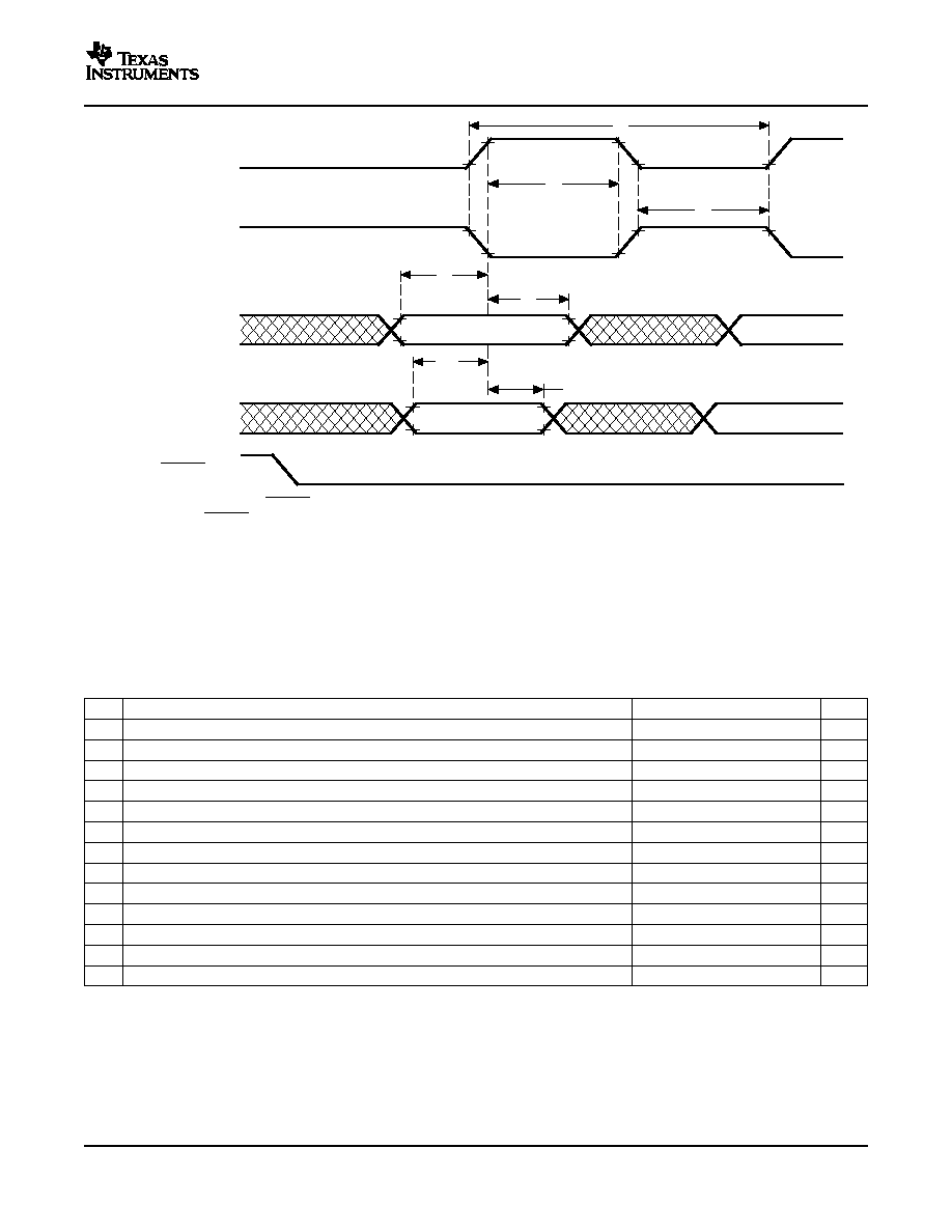
www.ti.com
Data Valid
11
SPISOMI
SPISIMO
SPICLK
(clock polarity = 1)
SPICLK
(clock polarity = 0)
Master In Data Must
Be Valid
Master Out Data Is Valid
1
7
6
10
3
2
SPISTE
(A)
6.9.6
SPI Slave Mode Timing
TMS320F2809, TMS320F2808, TMS320F2806
TMS320F2802, TMS320F2801, UCD9501
TMS320C2802, TMS320C2801 Digital Signal Processors
SPRS230G ≠ OCTOBER 2003 ≠ REVISED FEBRUARY 2006
A.
In the master mode, SPISTE goes active 0.5t
c(SPC)
(minimum) before valid SPI clock edge. On the trailing end of the
word, the SPISTE will go inactive 0.5t
c(SPC)
after the receiving edge (SPICLK) of the last data bit.
Figure 6-18. SPI Master External Timing (Clock Phase = 1)
Table 6-35
lists the slave mode external timing (clock phase = 0) and
Table 6-36
(clock phase = 1).
Figure 6-19
and
Figure 6-20
show the timing waveforms.
Table 6-35. SPI Slave Mode External Timing (Clock Phase = 0)
(1) (2) (3) (4) (5)
NO.
MIN
MAX
UNIT
12
t
c(SPC)S
Cycle time, SPICLKCycle time, SPICLK
4t
c(LCO)
ns
13
t
w(SPCH)S
Pulse duration, SPICLK high (clock polarity = 0)
0.5t
c(SPC)S
- 10
0.5t
c(SPC)S
ns
t
w(SPCL)S
Pulse duration, SPICLK low (clock polarity = 1)
0.5t
c(SPC)S
- 10
0.5t
c(SPC)S
ns
14
t
w(SPCL)S
Pulse duration, SPICLK low (clock polarity = 0)
0.5t
c(SPC)S
- 10
0.5t
c(SPC)S
ns
t
w(SPCH)S
Pulse duration, SPICLK high (clock polarity = 1)
0.5t
c(SPC)S
- 10
0.5t
c(SPC)S
ns
15
t
d(SPCH-SOMI)S
Delay time, SPICLK high to SPISOMI valid (clock polarity = 0)
35
ns
t
d(SPCL-SOMI)S
Delay time, SPICLK low to SPISOMI valid (clock polarity = 1)
35
ns
16
t
v(SPCL-SOMI)S
Valid time, SPISOMI data valid after SPICLK low (clock polarity = 0)
0.75t
c(SPC)S
ns
t
v(SPCH-SOMI)S
Valid time, SPISOMI data valid after SPICLK high (clock polarity = 1)
0.75t
c(SPC)S
ns
19
t
su(SIMO-SPCL)S
Setup time, SPISIMO before SPICLK low (clock polarity = 0)
35
ns
t
su(SIMO-SPCH)S
Setup time, SPISIMO before SPICLK high (clock polarity = 1)
35
ns
20
t
v(SPCL-SIMO)S
Valid time, SPISIMO data valid after SPICLK low (clock polarity = 0)
0.5t
c(SPC)S
ns
t
v(SPCH-SIMO)S
Valid time, SPISIMO data valid after SPICLK high (clock polarity = 1)
0.5t
c(SPC)S
ns
(1)
The MASTER / SLAVE bit (SPICTL.2) is cleared and the CLOCK PHASE bit (SPICTL.3) is cleared.
(2)
t
c(SPC)
= SPI clock cycle time = LSPCLK/4 or LSPCLK/(SPIBRR + 1)
(3)
Internal clock prescalers must be adjusted such that the SPI clock speed is limited to the following SPI clock rate:
Master mode transmit 25-MHz MAX, master mode receive 12.5-MHz MAX
Slave mode transmit 12.5-MHz MAX, slave mode receive 12.5-MHz MAX.
(4)
t
c(LCO)
= LSPCLK cycle time
(5)
The active edge of the SPICLK signal referenced is controlled by the CLOCK POLARITY bit (SPICCR.6).
Electrical Specifications
115
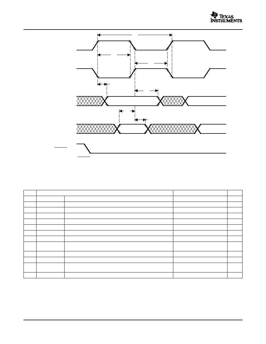
www.ti.com
20
15
SPISIMO
SPISOMI
SPICLK
(clock polarity = 1)
SPICLK
(clock polarity = 0)
SPISIMO Data
Must Be Valid
SPISOMI Data Is Valid
19
16
14
13
12
SPISTE
(A)
TMS320F2809, TMS320F2808, TMS320F2806
TMS320F2802, TMS320F2801, UCD9501
TMS320C2802, TMS320C2801 Digital Signal Processors
SPRS230G ≠ OCTOBER 2003 ≠ REVISED FEBRUARY 2006
A.
In the slave mode, the SPISTE signal should be asserted low at least 0.5t
c(SPC)
(minimum) before the valid SPI clock
edge and remain low for at least 0.5t
c(SPC)
after the receiving edge (SPICLK) of the last data bit.
Figure 6-19. SPI Slave Mode External Timing (Clock Phase = 0)
Table 6-36. SPI Slave Mode External Timing (Clock Phase = 1)
(1) (2) (3) (4)
NO.
MIN
MAX
UNIT
12
t
c(SPC)S
Cycle time, SPICLK
8t
c(LCO)
ns
13
t
w(SPCH)S
Pulse duration, SPICLK high (clock polarity = 0)
0.5t
c(SPC)S
- 10
0.5t
c(SPC)S
ns
t
w(SPCL)S
Pulse duration, SPICLK low (clock polarity = 1)
0.5t
c(SPC)S
- 10
0.5t
c(SPC)S
ns
14
t
w(SPCL)S
Pulse duration, SPICLK low (clock polarity = 0)
0.5t
c(SPC)S
- 10
0.5t
c(SPC)S
ns
t
w(SPCH)S
Pulse duration, SPICLK high (clock polarity = 1)
0.5t
c(SPC)S
- 10
0.5t
c(SPC)S
ns
17
t
su(SOMI-SPCH)S
Setup time, SPISOMI before SPICLK high (clock polarity = 0)
0.125t
c(SPC)S
ns
t
su(SOMI-SPCL)S
Setup time, SPISOMI before SPICLK low (clock polarity = 1
0.125t
c(SPC)S
ns
18
t
v(SPCH-SOMI)S
Valid time, SPISOMI data valid after SPICLK low (clock polarity = 0)
0.75t
c(SPC)S
ns
t
v(SPCL-SOMI)S
Valid time, SPISOMI data valid after SPICLK high
0.75t
c(SPC)S
ns
(clock polarity = 1)
21
t
su(SIMO-SPCH)S
Setup time, SPISIMO before SPICLK high (clock polarity = 0)
35
ns
t
su(SIMO-SPCL)S
Setup time, SPISIMO before SPICLK low (clock polarity = 1)
35
ns
22
t
v(SPCH-SIMO)S
Valid time, SPISIMO data valid after SPICLK high
0.5t
c(SPC)S
ns
(clock polarity = 0)
t
v(SPCL-SIMO)S
Valid time, SPISIMO data valid after SPICLK low (clock polarity = 1)
0.5t
c(SPC)S
ns
(1)
The MASTER / SLAVE bit (SPICTL.2) is cleared and the CLOCK PHASE bit (SPICTL.3) is cleared.
(2)
t
c(SPC)
= SPI clock cycle time = LSPCLK/4 or LSPCLK/(SPIBRR + 1)
(3)
Internal clock prescalers must be adjusted such that the SPI clock speed is limited to the following SPI clock rate:
Master mode transmit 25-MHz MAX, master mode receive 12.5-MHz MAX
Slave mode transmit 12.5-MHz MAX, slave mode receive 12.5-MHz MAX.
(4)
The active edge of the SPICLK signal referenced is controlled by the CLOCK POLARITY bit (SPICCR.6).
Electrical Specifications
116
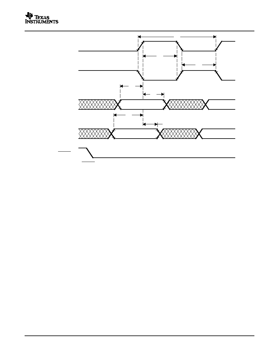
www.ti.com
Data Valid
22
SPISIMO
SPISOMI
SPICLK
(clock polarity = 1)
SPICLK
(clock polarity = 0)
SPISIMO Data
Must Be Valid
SPISOMI Data Is Valid
21
12
18
17
14
13
SPISTE
(A)
TMS320F2809, TMS320F2808, TMS320F2806
TMS320F2802, TMS320F2801, UCD9501
TMS320C2802, TMS320C2801 Digital Signal Processors
SPRS230G ≠ OCTOBER 2003 ≠ REVISED FEBRUARY 2006
A.
In the slave mode, the SPISTE signal should be asserted low at least 0.5t
c(SPC)
before the valid SPI clock edge and
remain low for at least 0.5t
c(SPC)
after the receiving edge (SPICLK) of the last data bit.
Figure 6-20. SPI Slave Mode External Timing (Clock Phase = 1)
Electrical Specifications
117
www.ti.com
6.9.7
On-Chip Analog-to-Digital Converter
TMS320F2809, TMS320F2808, TMS320F2806
TMS320F2802, TMS320F2801, UCD9501
TMS320C2802, TMS320C2801 Digital Signal Processors
SPRS230G ≠ OCTOBER 2003 ≠ REVISED FEBRUARY 2006
Table 6-37. ADC Electrical Characteristics (over recommended operating conditions)
(1) (2)
PARAMETER
MIN
TYP
MAX
UNIT
DC SPECIFICATIONS
Resolution
12
Bits
ADC clock
1
kHz
12.5
MHz
ACCURACY
INL (Integral nonlinearity)
1-12.5 MHz ADC clock (6.25 MSPS)
±
1.5
LSB
DNL (Differential nonlinearity)
(3)
1-12.5 MHz ADC clock (6.25 MSPS)
±
1
LSB
Offset error
(4)
-60
+60
LSB
Offset error with hardware trimming
±
4
LSB
Overall gain error with internal reference
(5)
-60
+60
LSB
Overall gain error with external reference
-60
+60
LSB
Channel-to-channel offset variation
±
4
LSB
Channel-to-channel gain variation
±
4
LSB
ANALOG INPUT
Analog input voltage (ADCINx to ADCLO)
(6)
0
3
V
ADCLO
-5
0
5
mV
Input capacitance
10
pF
Input leakage current
±
5
µ
A
INTERNAL VOLTAGE REFERENCE
(5)
V
ADCREFP
- ADCREFP output voltage at the pin based on
1.275
V
internal reference
V
ADCREFM
- ADCREFM output voltage at the pin based on
0.525
V
internal reference
Voltage difference, ADCREFP - ADCREFM
0.75
V
Temperature coefficient
50
PPM/
∞
C
EXTERNAL VOLTAGE REFERENCE
(5) (7)
ADCREFSEL[15:14] = 11b
1.024
V
V
ADCREFIN
- External reference voltage input on ADCREFIN
ADCREFSEL[15:14] = 10b
1.500
V
pin 0.2% or better accurate reference recommended
ADCREFSEL[15:14] = 01b
2.048
V
AC SPECIFICATIONS
SINAD (100 kHz) Signal-to-noise ratio + distortion
67.5
dB
SNR (100 kHz) Signal-to-noise ratio
68
dB
THD (100 kHz) Total harmonic distortion
-79
dB
ENOB (100 kHz) Effective number of bits
10.9
Bits
SFDR (100 kHz) Spurious free dynamic range
83
dB
(1)
Tested at 12.5 MHz ADCCLK.
(2)
All voltages listed in this table are with respect to V
SSA2
.
(3)
TI specifies that the ADC will have no missing codes.
(4)
1 LSB has the weighted value of 3.0/4096 = 0.732 mV.
(5)
A single internal/external band gap reference sources both ADCREFP and ADCREFM signals, and hence, these voltages track
together. The ADC converter uses the difference between these two as its reference. The total gain error listed for the internal reference
is inclusive of the movement of the internal bandgap over temperature. Gain error over temperature for the external reference option will
depend on the temperature profile of the source used.
(6)
Voltages above V
DDA
+ 0.3 V or below V
SS
- 0.3 V applied to an analog input pin may temporarily affect the conversion of another pin.
To avoid this, the analog inputs should be kept within these limits.
(7)
TI recommends using high precision external reference TI part REF3020/3120 or equivalent for 2.048-V reference.
Electrical Specifications
118
www.ti.com
6.9.7.1
ADC Power-Up Control Bit Timing
ADC Power Up Delay
ADC Ready for Conversions
PWDNBG
PWDNREF
PWDNADC
Request for
ADC
Conversion
t
d(BGR)
t
d(PWD)
TMS320F2809, TMS320F2808, TMS320F2806
TMS320F2802, TMS320F2801, UCD9501
TMS320C2802, TMS320C2801 Digital Signal Processors
SPRS230G ≠ OCTOBER 2003 ≠ REVISED FEBRUARY 2006
Figure 6-21. ADC Power-Up Control Bit Timing
Table 6-38. ADC Power-Up Delays
PARAMETER
(1)
MIN
TYP
MAX
UNIT
t
d(BGR)
Delay time for band gap reference to be stable. Bits 7 and 6 of the ADCTRL3
5
ms
register (ADCBGRFDN1/0) must be set to 1 before the PWDNADC bit is enabled.
t
d(PWD)
Delay time for power-down control to be stable. Bit delay time for band-gap
20
50
µ
s
reference to be stable. Bits 7 and 6 of the ADCTRL3 register (ADCBGRFDN1/0)
1
ms
must be set to 1 before the PWDNADC bit is enabled. Bit 5 of the ADCTRL3
register (PWDNADC)must be set to 1 before any ADC conversions are initiated.
(1)
Timings maintain compatibility to the 281x ADC module. The 280x ADC also supports driving all 3 bits at the same time and waiting
t
d(BGR)
ms before first conversion.
Table 6-39. Current Consumption for Different ADC Configurations (at 12.5-MHz ADCCLK)
(1) (2)
ADC OPERATING MODE
CONDITIONS
V
DDA18
V
DDA3.3
UNIT
Mode A (Operational Mode):
30
2
mA
∑
BG and REF enabled
∑
PWD disabled
Mode B:
9
0.5
mA
∑
ADC clock enabled
∑
BG and REF enabled
∑
PWD enabled
Mode C:
5
20
µ
A
∑
ADC clock enabled
∑
BG and REF disabled
∑
PWD enabled
Mode D:
5
15
µ
A
∑
ADC clock disabled
∑
BG and REF disabled
∑
PWD enabled
(1)
Test Conditions:
SYSCLKOUT = 100 MHz
ADC module clock = 12.5 MHz
ADC performing a continuous conversion of all 16 channels in Mode A
(2)
V
DDA18
includes current into V
DD1A18
and V
DD2A18
. V
DDA3.3
includes current into V
DDA2
and V
DDAIO
.
Electrical Specifications
119
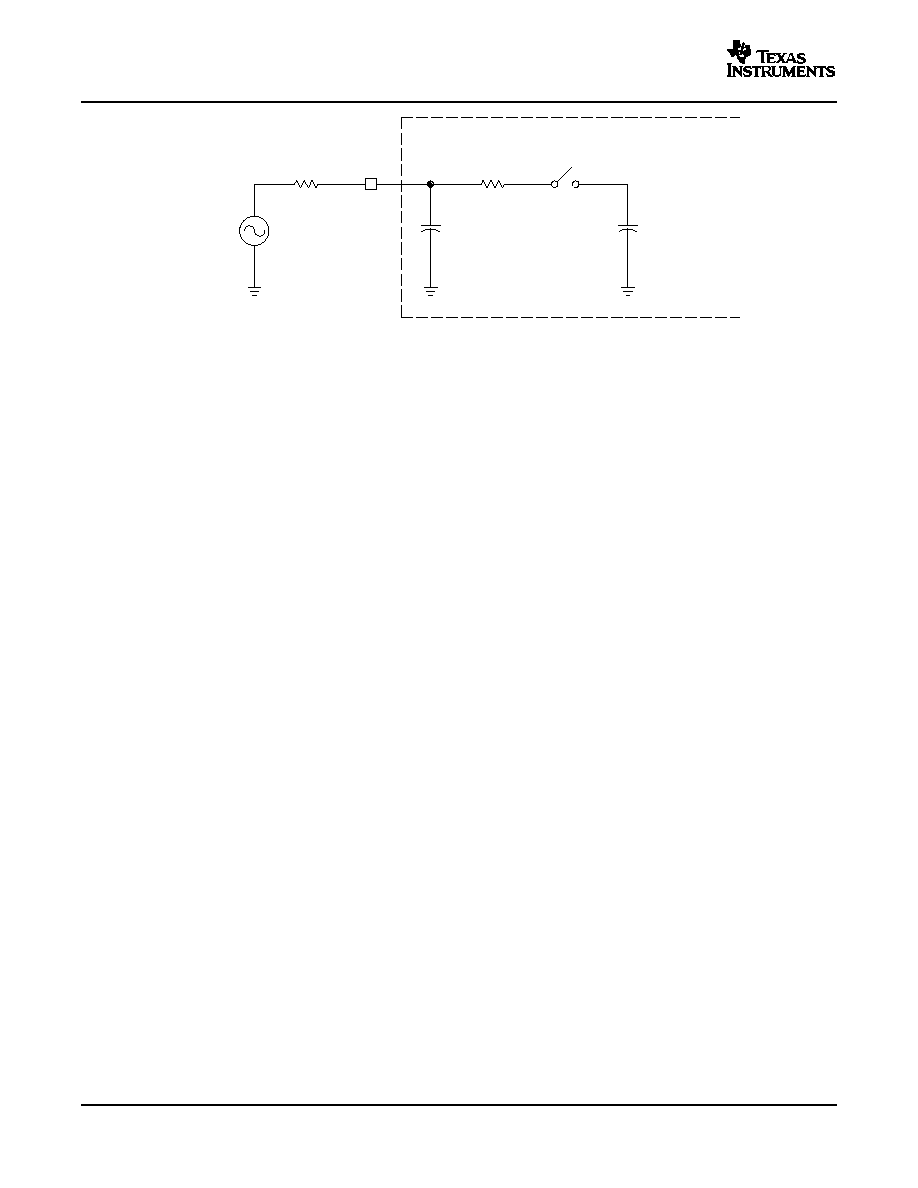
www.ti.com
ac
R
s
ADCIN0
C
p
10 pF
R
on
1 k
1.64 pF
C
h
Switch
Typical Values of the Input Circuit Components:
Switch Resistance (R
on
):
1 k
Sampling Capacitor (C
h
):
1.64 pF
Parasitic Capacitance (C
p
): 10 pF
Source Resistance (R
s
):
50
28x DSP
Source
Signal
6.9.7.2
Definitions
TMS320F2809, TMS320F2808, TMS320F2806
TMS320F2802, TMS320F2801, UCD9501
TMS320C2802, TMS320C2801 Digital Signal Processors
SPRS230G ≠ OCTOBER 2003 ≠ REVISED FEBRUARY 2006
Figure 6-22. ADC Analog Input Impedance Model
Reference Voltage
The on-chip ADC has a built-in reference, which provides the reference voltages for the ADC.
Analog Inputs
The on-chip ADC consists of 16 analog inputs, which are sampled either one at a time or two channels at
a time. These inputs are software-selectable.
Converter
The on-chip ADC uses a 12-bit four-stage pipeline architecture, which achieves a high sample rate with
low power consumption.
Conversion Modes
The conversion can be performed in two different conversion modes:
∑
Sequential sampling mode (SMODE = 0)
∑
Simultaneous sampling mode (SMODE = 1)
Electrical Specifications
120
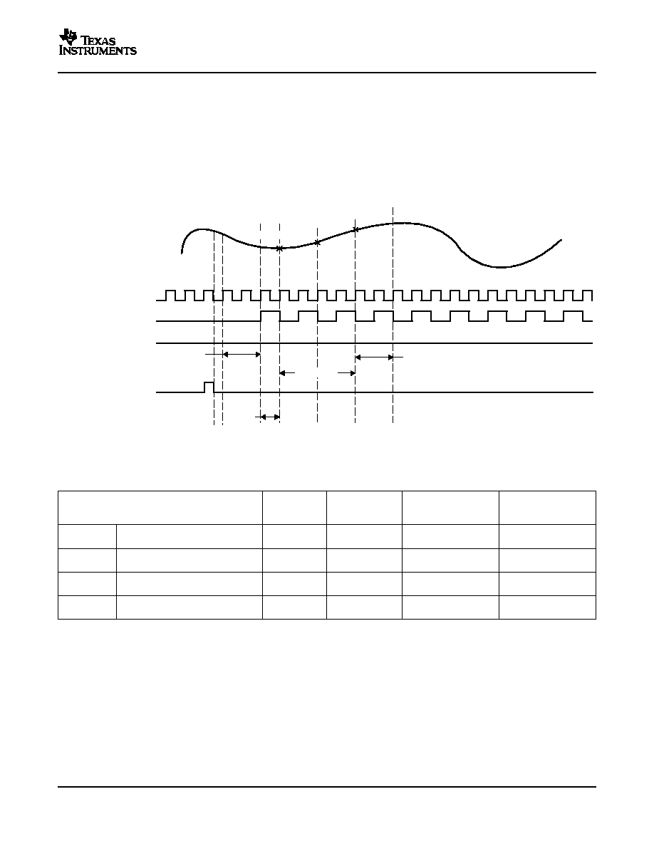
www.ti.com
6.9.7.3
Sequential Sampling Mode (Single-Channel) (SMODE = 0)
Analog Input on
Channel Ax or Bx
ADC Clock
Sample and Hold
SH Pulse
SMODE Bit
t
dschx_n
t
dschx_n+1
Sample n
Sample n+1
Sample n+2
t
SH
ADC Event Trigger from
ePWM or Other Sources
t
d(SH)
TMS320F2809, TMS320F2808, TMS320F2806
TMS320F2802, TMS320F2801, UCD9501
TMS320C2802, TMS320C2801 Digital Signal Processors
SPRS230G ≠ OCTOBER 2003 ≠ REVISED FEBRUARY 2006
In sequential sampling mode, the ADC can continuously convert input signals on any of the channels (Ax
to Bx). The ADC can start conversions on event triggers from the ePWM, software trigger, or from an
external ADCSOC signal. If the SMODE bit is 0, the ADC will do conversions on the selected channel on
every Sample/Hold pulse. The conversion time and latency of the Result register update are explained
below. The ADC interrupt flags are set a few SYSCLKOUT cycles after the Result register update. The
selected channels will be sampled at every falling edge of the Sample/Hold pulse. The Sample/Hold pulse
width can be programmed to be 1 ADC clock wide (minimum) or 16 ADC clocks wide (maximum).
Figure 6-23. Sequential Sampling Mode (Single-Channel) Timing
Table 6-40. Sequential Sampling Mode Timing
AT 12.5 MHz
SAMPLE n
SAMPLE n + 1
ADC CLOCK,
REMARKS
t
c(ADCCLK)
= 80 ns
t
d(SH)
Delay time from event trigger to
2.5t
c(ADCCLK)
sampling
t
SH
Sample/Hold width/Acquisition
(1 + Acqps) *
80 ns with Acqps = 0
Acqps value = 0-15
Width
t
c(ADCCLK)
ADCTRL1[8:11]
t
d(schx_n)
Delay time for first result to appear
4t
c(ADCCLK)
320 ns
in Result register
t
d(schx_n+1)
Delay time for successive results to
(2 + Acqps) *
160 ns
appear in Result register
t
c(ADCCLK)
Electrical Specifications
121
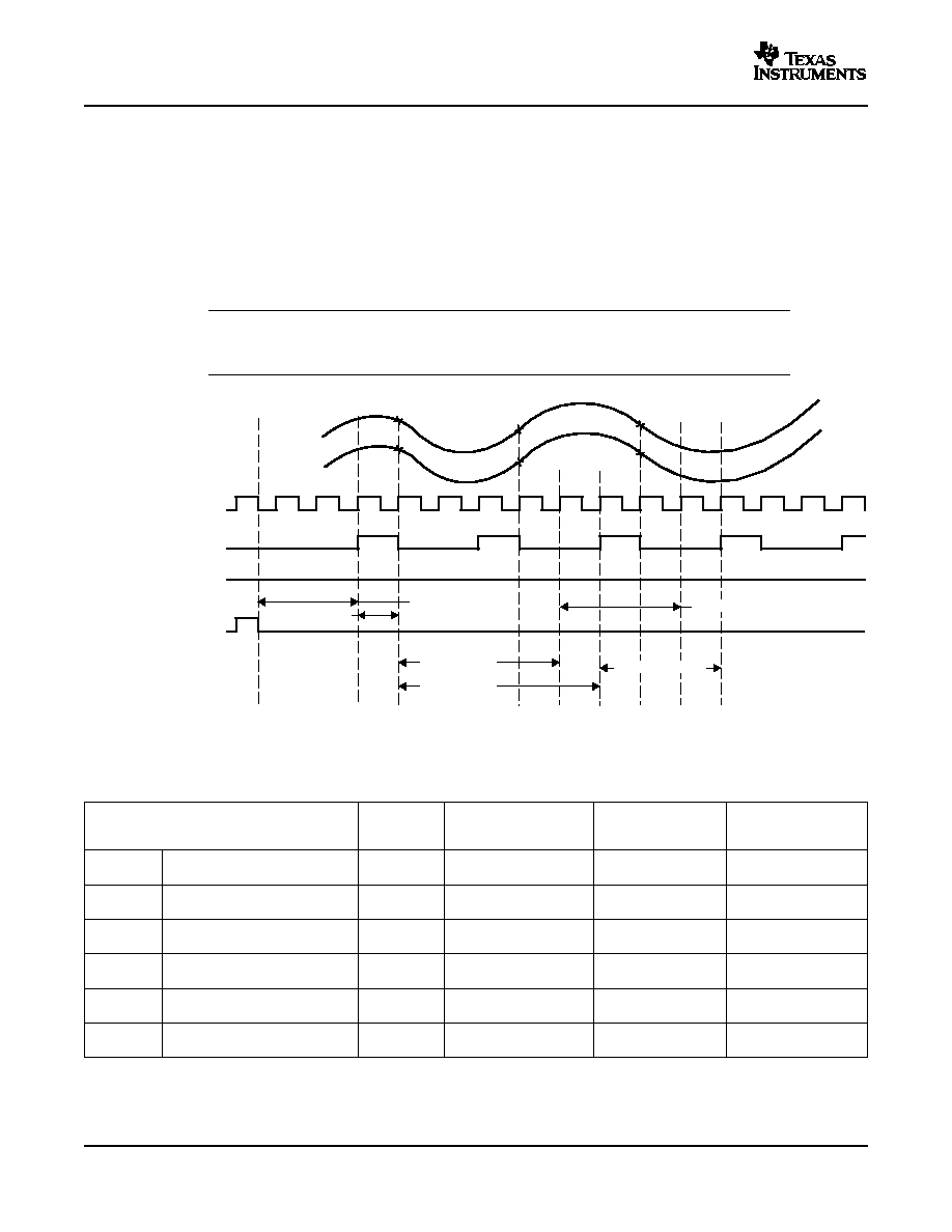
www.ti.com
6.9.7.4
Simultaneous Sampling Mode (Dual-Channel) (SMODE = 1)
Analog Input on
Channel Ax
Analog Input on
Channel Bx
ADC Clock
Sample and Hold
SH Pulse
t
SH
t
dschA0_n
t
dschB0_n
t
dschB0_n+1
Sample n
Sample n+1
Sample n+2
t
dschA0_n+1
t
d(SH)
ADC Event Trigger from
ePWM or Other Sources
SMODE Bit
TMS320F2809, TMS320F2808, TMS320F2806
TMS320F2802, TMS320F2801, UCD9501
TMS320C2802, TMS320C2801 Digital Signal Processors
SPRS230G ≠ OCTOBER 2003 ≠ REVISED FEBRUARY 2006
In simultaneous mode, the ADC can continuously convert input signals on any one pair of channels
(A0/B0 to A7/B7). The ADC can start conversions on event triggers from the ePWM, software trigger, or
from an external ADCSOC signal. If the SMODE bit is 1, the ADC will do conversions on two selected
channels on every Sample/Hold pulse. The conversion time and latency of the result register update are
explained below. The ADC interrupt flags are set a few SYSCLKOUT cycles after the Result register
update. The selected channels will be sampled simultaneously at the falling edge of the Sample/Hold
pulse. The Sample/Hold pulse width can be programmed to be 1 ADC clock wide (minimum) or 16 ADC
clocks wide (maximum).
NOTE
In simultaneous mode, the ADCIN channel pair select has to be A0/B0, A1/B1, ..., A7/B7,
and not in other combinations (such as A1/B3, etc.).
Figure 6-24. Simultaneous Sampling Mode Timing
Table 6-41. Simultaneous Sampling Mode Timing
AT 12.5 MHz
SAMPLE n
SAMPLE n + 1
ADC CLOCK,
REMARKS
t
c(ADCCLK)
= 80 ns
t
d(SH)
Delay time from event trigger to
2.5t
c(ADCCLK)
sampling
t
SH
Sample/Hold width/Acquisition
(1 + Acqps) *
80 ns with Acqps = 0
Acqps value = 0-15
Width
t
c(ADCCLK)
ADCTRL1[8:11]
t
d(schA0_n)
Delay time for first result to
4t
c(ADCCLK)
320 ns
appear in Result register
t
d(schB0_n)
Delay time for first result to
5t
c(ADCCLK)
400 ns
appear in Result register
t
d(schA0_n+1)
Delay time for successive results
(3 + Acqps) * t
c(ADCCLK)
240 ns
to appear in Result register
t
d(schB0_n+1)
Delay time for successive results
(3 + Acqps) * t
c(ADCCLK)
240 ns
to appear in Result register
Electrical Specifications
122

www.ti.com
6.10
Detailed Descriptions
formula,
N
+
(SINAD
*
1.76)
6.02
it is possible to get a measure of performance expressed as N, the effective
TMS320F2809, TMS320F2808, TMS320F2806
TMS320F2802, TMS320F2801, UCD9501
TMS320C2802, TMS320C2801 Digital Signal Processors
SPRS230G ≠ OCTOBER 2003 ≠ REVISED FEBRUARY 2006
Integral Nonlinearity
Integral nonlinearity refers to the deviation of each individual code from a line drawn from zero through full
scale. The point used as zero occurs one-half LSB before the first code transition. The full-scale point is
defined as level one-half LSB beyond the last code transition. The deviation is measured from the center
of each particular code to the true straight line between these two points.
Differential Nonlinearity
An ideal ADC exhibits code transitions that are exactly 1 LSB apart. DNL is the deviation from this ideal
value. A differential nonlinearity error of less than
±
1 LSB ensures no missing codes.
Zero Offset
The major carry transition should occur when the analog input is at zero volts. Zero error is defined as the
deviation of the actual transition from that point.
Gain Error
The first code transition should occur at an analog value one-half LSB above negative full scale. The last
transition should occur at an analog value one and one-half LSB below the nominal full scale. Gain error is
the deviation of the actual difference between first and last code transitions and the ideal difference
between first and last code transitions.
Signal-to-Noise Ratio + Distortion (SINAD)
SINAD is the ratio of the rms value of the measured input signal to the rms sum of all other spectral
components below the Nyquist frequency, including harmonics but excluding dc. The value for SINAD is
expressed in decibels.
Effective Number of Bits (ENOB)
For a sine wave, SINAD can be expressed in terms of the number of bits. Using the following
number of bits. Thus, effective number of bits for a device for sine wave inputs at a given input frequency
can be calculated directly from its measured SINAD.
Total Harmonic Distortion (THD)
THD is the ratio of the rms sum of the first nine harmonic components to the rms value of the measured
input signal and is expressed as a percentage or in decibels.
Spurious Free Dynamic Range (SFDR)
SFDR is the difference in dB between the rms amplitude of the input signal and the peak spurious signal.
Electrical Specifications
123
www.ti.com
6.11
Flash Timing
Page Wait State
+
t
a(fp)
t
c(SCO)
*
1
(round up to the next highest integer) or 0, whichever is larger
Random Wait State
+
t
a(fr)
t
c(SCO)
*
1
(round up to the next highest integer) or 1, whichever is larger
TMS320F2809, TMS320F2808, TMS320F2806
TMS320F2802, TMS320F2801, UCD9501
TMS320C2802, TMS320C2801 Digital Signal Processors
SPRS230G ≠ OCTOBER 2003 ≠ REVISED FEBRUARY 2006
Table 6-42. Flash Endurance
MIN
TYP
MAX
UNIT
N
f
Flash endurance for the array (write/erase cycles)
0
∞
C to 85
∞
C (ambient)
100
1000
cycles
N
OTP
OTP endurance for the array (write cycles)
0
∞
C to 85
∞
C (ambient)
1
write
Table 6-43. Flash Parameters at 100-MHz SYSCLKOUT
PARAMETER
(1)
TEST CONDITIONS
MIN
TYP
MAX
UNIT
Program
16-Bit Word
50
µ
s
Time
16K Sector
500
ms
8K Sector
250
ms
4K Sector
125
ms
Erase Time
16K Sector
10
S
8K Sector
10
S
4K Sector
10
S
I
DD3VFLP
V
DD3VFL
current consumption during the
Erase
75
mA
Erase/Program cycle
Program
35
mA
I
DDP
V
DD
current consumption during Erase/Program
140
mA
cycle
I
DDIOP
V
DDIO
current consumption during Erase/Program
20
mA
cycle
(1)
Typical parameters as seen at room temperature using flash API version 3.00 including function call overhead.
Table 6-44. Flash/OTP Access Timing
PARAMETER
(1)
MIN
TYP
MAX
UNIT
t
a(fp)
Paged flash access time
36
ns
t
a(fr)
Random flash access time
36
ns
t
a(OTP)
OTP access time
60
ns
(1)
For 100 MHz, PAGE WS = 3 and RANDOM WS = 3; for 75 MHz, PAGE WS = 2, and RANDOM WS = 2.
Equations to compute the page wait state and random wait state in
Table 6-45
are as follows:
Electrical Specifications
124
www.ti.com
6.12
ROM Timing
Page Wait State
+
t
a(rp)
t
c(SCO)
*
1
(round up to the next highest integer) or 0, whichever is larger
Random Wait State
+
t
a(rr)
t
c(SCO)
*
1
(round up to the next highest integer) or 1, whichever is larger
TMS320F2809, TMS320F2808, TMS320F2806
TMS320F2802, TMS320F2801, UCD9501
TMS320C2802, TMS320C2801 Digital Signal Processors
SPRS230G ≠ OCTOBER 2003 ≠ REVISED FEBRUARY 2006
Table 6-45. Minimum Required Wait-States at Different Frequencies
SYSCLKOUT (MHz)
SYSCLKOUT (ns)
PAGE WAIT-STATE
RANDOM WAIT STATE
(1)
100
10
3
3
75
13.33
2
2
50
20
1
1
30
33.33
1
1
25
40
0
1
15
66.67
0
1
4
250
0
1
(1)
Random wait state must be greater than or equal to 1.
Table 6-46. ROM/OTP Access Timing
PARAMETER
(1)
MIN
TYP
MAX
UNIT
t
a(rp)
Paged ROM access time
19
ns
t
a(rr)
Random ROM access time
19
ns
t
a(OTP)
OTP access time
60
ns
(1)
For 100 MHz, PAGE WS = 1 and RANDOM WS = 1; for 75 MHz, PAGE WS = 1, and RANDOM WS = 1.
Equations to compute the page wait state and random wait state in
Table 6-47
are as follows:
Table 6-47. Minimum Required Wait-States at Different Frequencies
SYSCLKOUT (MHz)
SYSCLKOUT (ns)
PAGE WAIT-STATE
RANDOM WAIT STATE
(1)
100
10
1
1
75
13.33
1
1
50
20
0
1
30
33.33
0
1
25
40
0
1
15
66.67
0
1
4
250
0
1
(1)
Random wait state must be greater than or equal to 1.
Electrical Specifications
125

www.ti.com
7
Migrating From F280x Devices to C280x Devices
7.1
Migration Issues
TMS320F2809, TMS320F2808, TMS320F2806
TMS320F2802, TMS320F2801, UCD9501
TMS320C2802, TMS320C2801 Digital Signal Processors
SPRS230G ≠ OCTOBER 2003 ≠ REVISED FEBRUARY 2006
The migration issues to be considered while migrating from the F280x devices to C280x devices are as
follows:
∑
The 1K OTP memory available in F280x devices has been replaced by 1K ROM C280x devices.
∑
Current consumption differs for F280x and C280x devices for all four possible modes. See the
appropriate electrical section for exact numbers.
∑
The V
DD3VFL
pin is the 3.3-V Flash core power pin in F280x devices but is a V
DDIO
pin in C280x
devices.
∑
F280x and C280x devices are pin-compatible and code-compatible; however, they are electrically
different with different EMI/ESD profiles. Before ramping production with C280x devices, evaluate
performance of the hardware design with both devices.
∑
Addresses 0x3D 7BFC through 0x3D 7BFF in the OTP and addresses 0x3F 7FF2 through 0x3F 7FF5
in the main ROM array are reserved for ROM part-specific information and are not available for user
applications.
∑
The paged and random wait-state specifications for the Flash and ROM parts are different. While
migrating from Flash to ROM parts, the same wait-state values must be used for best-performance
compatibility (for example, in applications that use software delay loops or where precise interrupt
latencies are critical).
∑
The analog input switch resistance is smaller in C280x devices compared to F280x devices. While
migrating from a Flash to a ROM device care should be taken to design the analog input circuits to
meet the application performance required by the sampling network.
∑
The PART-ID register value is different for Flash and ROM parts.
For errata applicable to 280x devices, see the
TMS320F2808, TMS320F2806, TMS320F2802,
TMS320F2801, UCD9501, TMS320C2802, TMS320C2801 DSP Silicon Errata
(literature number
SPRZ171).
Migrating From F280x Devices to C280x Devices
126
www.ti.com
8
Mechanical Data
TMS320F2809, TMS320F2808, TMS320F2806
TMS320F2802, TMS320F2801, UCD9501
TMS320C2802, TMS320C2801 Digital Signal Processors
SPRS230G ≠ OCTOBER 2003 ≠ REVISED FEBRUARY 2006
Table 8-1
,
Table 8-2
,
Table 8-3
, and
Table 8-4
show the thermal data.
The mechanical package diagram(s) that follow the tables reflect the most current released mechanical
data available for the designated device(s).
Table 8-1. F280x, UCD9501 Thermal Model 100-pin GGM Results
AIR FLOW
PARAMETER
0 lfm
150 lfm
250 lfm
500 lfm
JA
[
∞
C/W] High k PCB
30.58
29.31
28.09
26.62
JT
[
∞
C/W]
0.4184
0.32
0.3725
0.4887
JC
12.08
JB
16.46
Table 8-2. F280x, UCD9501 Thermal Model 100-pin PZ Results
AIR FLOW
PARAMETER
0 lfm
150 lfm
250 lfm
500 lfm
JA
[
∞
C/W] High k PCB
48.16
40.06
37.96
35.17
JT
[
∞
C/W]
0.3425
0.85
1.0575
1.410
JC
12.89
JB
29.58
Table 8-3. C280x Thermal Model 100-pin GGM Results
AIR FLOW
PARAMETER
0 lfm
150 lfm
250 lfm
500 lfm
JA
[
∞
C/W] High k PCB
36.33
35.01
33.81
32.31
JT
[
∞
C/W]
0.57
0.43
0.52
0.67
JC
14.18
JB
21.36
Table 8-4. C280x Thermal Model 100-pin PZ Results
AIR FLOW
PARAMETER
0 lfm
150 lfm
250 lfm
500 lfm
JA
[
∞
C/W] High k PCB
69.81
60.34
57.46
53.63
JT
[
∞
C/W]
0.42
1.23
1.54
2.11
JC
13.52
JB
54.78
Mechanical Data
127
PACKAGING INFORMATION
Orderable Device
Status
(1)
Package
Type
Package
Drawing
Pins Package
Qty
Eco Plan
(2)
Lead/Ball Finish
MSL Peak Temp
(3)
TMS320C2801GGMA
ACTIVE
BGA
GGM
100
TBD
Call TI
Call TI
TMS320C2801GGMS
ACTIVE
BGA
GGM
100
TBD
Call TI
Call TI
TMS320C2801PZA
ACTIVE
LQFP
PZ
100
TBD
Call TI
Call TI
TMS320C2801PZQ
ACTIVE
LQFP
PZ
100
TBD
Call TI
Call TI
TMS320C2801PZS
ACTIVE
LQFP
PZ
100
TBD
Call TI
Call TI
TMS320C2801ZGMA
ACTIVE
BGA MI
CROSTA
R
ZGM
100
TBD
Call TI
Call TI
TMS320C2801ZGMS
ACTIVE
BGA MI
CROSTA
R
ZGM
100
TBD
Call TI
Call TI
TMS320C2802GGMA
ACTIVE
BGA
GGM
100
TBD
Call TI
Call TI
TMS320C2802GGMS
ACTIVE
BGA
GGM
100
TBD
Call TI
Call TI
TMS320C2802PZA
ACTIVE
LQFP
PZ
100
TBD
Call TI
Call TI
TMS320C2802PZQ
ACTIVE
LQFP
PZ
100
TBD
Call TI
Call TI
TMS320C2802PZS
ACTIVE
LQFP
PZ
100
TBD
Call TI
Call TI
TMS320C2802ZGMA
ACTIVE
BGA MI
CROSTA
R
ZGM
100
TBD
Call TI
Call TI
TMS320C2802ZGMS
ACTIVE
BGA MI
CROSTA
R
ZGM
100
TBD
Call TI
Call TI
TMS320F2801GGMA
ACTIVE
BGA
GGM
100
184
TBD
SNPB
Level-3-220C-168HR
TMS320F2801GGMS
ACTIVE
BGA
GGM
100
184
TBD
SNPB
Level-3-220C-168HR
TMS320F2801PZA
ACTIVE
LQFP
PZ
100
1
Green (RoHS &
no Sb/Br)
CU NIPDAU
Level-2-260C-1YR
TMS320F2801PZQ
ACTIVE
LQFP
PZ
100
90
TBD
Call TI
Call TI
TMS320F2801PZS
ACTIVE
LQFP
PZ
100
90
Green (RoHS &
no Sb/Br)
CU NIPDAU
Level-2-260C-1YR
TMS320F2801ZGMA
ACTIVE
BGA MI
CROSTA
R
ZGM
100
184
Green (RoHS &
no Sb/Br)
Call TI
Level-3-260C-168HR
TMS320F2801ZGMS
ACTIVE
BGA MI
CROSTA
R
ZGM
100
184
Green (RoHS &
no Sb/Br)
Call TI
Level-3-260C-168HR
TMS320F2802GGMA
ACTIVE
BGA
GGM
100
184
TBD
SNPB
Level-3-220C-168HR
TMS320F2802GGMS
ACTIVE
BGA
GGM
100
184
TBD
SNPB
Level-3-220C-168HR
TMS320F2802PZA
ACTIVE
LQFP
PZ
100
90
Green (RoHS &
no Sb/Br)
CU NIPDAU
Level-2-260C-1YR
TMS320F2802PZQ
ACTIVE
LQFP
PZ
100
90
Green (RoHS &
no Sb/Br)
CU NIPDAU
Level-2-260C-1YR
TMS320F2802PZS
ACTIVE
LQFP
PZ
100
90
Green (RoHS &
no Sb/Br)
CU NIPDAU
Level-2-260C-1YR
TMS320F2802ZGMA
ACTIVE
BGA MI
CROSTA
R
ZGM
100
184
Green (RoHS &
no Sb/Br)
Call TI
Level-3-260C-168HR
TMS320F2802ZGMS
ACTIVE
BGA MI
CROSTA
ZGM
100
184
Green (RoHS &
no Sb/Br)
Call TI
Level-3-260C-168HR
PACKAGE OPTION ADDENDUM
www.ti.com
6-Mar-2006
Addendum-Page 1
Orderable Device
Status
(1)
Package
Type
Package
Drawing
Pins Package
Qty
Eco Plan
(2)
Lead/Ball Finish
MSL Peak Temp
(3)
R
TMS320F2806GGMA
ACTIVE
BGA
GGM
100
184
TBD
SNPB
Level-3-220C-168HR
TMS320F2806GGMS
ACTIVE
BGA
GGM
100
184
TBD
SNPB
Level-3-220C-168HR
TMS320F2806PZA
ACTIVE
LQFP
PZ
100
1
Green (RoHS &
no Sb/Br)
CU NIPDAU
Level-2-260C-1YR
TMS320F2806PZQ
ACTIVE
LQFP
PZ
100
90
TBD
Call TI
Call TI
TMS320F2806PZS
ACTIVE
LQFP
PZ
100
90
Green (RoHS &
no Sb/Br)
CU NIPDAU
Level-2-260C-1YR
TMS320F2806ZGMA
ACTIVE
BGA MI
CROSTA
R
ZGM
100
184
Green (RoHS &
no Sb/Br)
Call TI
Level-3-260C-168HR
TMS320F2806ZGMS
ACTIVE
BGA MI
CROSTA
R
ZGM
100
184
TBD
Call TI
Call TI
TMS320F2808GGMA
ACTIVE
BGA
GGM
100
184
TBD
SNPB
Level-3-220C-168HR
TMS320F2808GGMS
ACTIVE
BGA
GGM
100
184
TBD
SNPB
Level-3-220C-168HR
TMS320F2808PZA
ACTIVE
LQFP
PZ
100
90
Green (RoHS &
no Sb/Br)
CU NIPDAU
Level-2-260C-1YR
TMS320F2808PZQ
ACTIVE
LQFP
PZ
100
90
Green (RoHS &
no Sb/Br)
CU NIPDAU
Level-2-260C-1YR
TMS320F2808PZS
ACTIVE
LQFP
PZ
100
90
Green (RoHS &
no Sb/Br)
CU NIPDAU
Level-2-260C-1YR
TMS320F2808ZGMA
ACTIVE
BGA MI
CROSTA
R
ZGM
100
184
Green (RoHS &
no Sb/Br)
Call TI
Level-3-260C-168HR
TMS320F2808ZGMS
ACTIVE
BGA MI
CROSTA
R
ZGM
100
184
Green (RoHS &
no Sb/Br)
Call TI
Level-3-260C-168HR
UCD9501PZA
ACTIVE
LQFP
PZ
100
1
TBD
Call TI
Call TI
UCD9501PZS
ACTIVE
LQFP
PZ
100
1
TBD
Call TI
Call TI
(1)
The marketing status values are defined as follows:
ACTIVE: Product device recommended for new designs.
LIFEBUY: TI has announced that the device will be discontinued, and a lifetime-buy period is in effect.
NRND: Not recommended for new designs. Device is in production to support existing customers, but TI does not recommend using this part in
a new design.
PREVIEW: Device has been announced but is not in production. Samples may or may not be available.
OBSOLETE: TI has discontinued the production of the device.
(2)
Eco Plan - The planned eco-friendly classification: Pb-Free (RoHS), Pb-Free (RoHS Exempt), or Green (RoHS & no Sb/Br) - please check
http://www.ti.com/productcontent
for the latest availability information and additional product content details.
TBD: The Pb-Free/Green conversion plan has not been defined.
Pb-Free (RoHS): TI's terms "Lead-Free" or "Pb-Free" mean semiconductor products that are compatible with the current RoHS requirements
for all 6 substances, including the requirement that lead not exceed 0.1% by weight in homogeneous materials. Where designed to be soldered
at high temperatures, TI Pb-Free products are suitable for use in specified lead-free processes.
Pb-Free (RoHS Exempt): This component has a RoHS exemption for either 1) lead-based flip-chip solder bumps used between the die and
package, or 2) lead-based die adhesive used between the die and leadframe. The component is otherwise considered Pb-Free (RoHS
compatible) as defined above.
Green (RoHS & no Sb/Br): TI defines "Green" to mean Pb-Free (RoHS compatible), and free of Bromine (Br) and Antimony (Sb) based flame
retardants (Br or Sb do not exceed 0.1% by weight in homogeneous material)
(3)
MSL, Peak Temp. -- The Moisture Sensitivity Level rating according to the JEDEC industry standard classifications, and peak solder
temperature.
PACKAGE OPTION ADDENDUM
www.ti.com
6-Mar-2006
Addendum-Page 2

Important Information and Disclaimer:The information provided on this page represents TI's knowledge and belief as of the date that it is
provided. TI bases its knowledge and belief on information provided by third parties, and makes no representation or warranty as to the
accuracy of such information. Efforts are underway to better integrate information from third parties. TI has taken and continues to take
reasonable steps to provide representative and accurate information but may not have conducted destructive testing or chemical analysis on
incoming materials and chemicals. TI and TI suppliers consider certain information to be proprietary, and thus CAS numbers and other limited
information may not be available for release.
In no event shall TI's liability arising out of such information exceed the total purchase price of the TI part(s) at issue in this document sold by TI
to Customer on an annual basis.
PACKAGE OPTION ADDENDUM
www.ti.com
6-Mar-2006
Addendum-Page 3
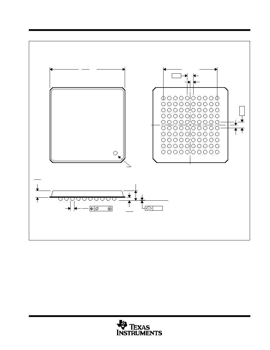
MECHANICAL DATA
MPBG028B FEBRUARY 1997 ≠ REVISED MAY 2002
1
POST OFFICE BOX 655303
∑
DALLAS, TEXAS 75265
GGM (S≠PBGA≠N100)
PLASTIC BALL GRID ARRAY
0,08
0,10
1,40 MAX
0,85
0,55
0,45
0,45
0,35
0,95
4
C
B
A
D
E
2
1
3
K
F
G
H
J
5
7
6
9
8
10
Seating Plane
SQ
9,90
10,10
7,20 TYP
0,40
0,40
A1 Corner
Bottom View
4145257≠3/C 12/01
0,80
0,80
NOTES: A. All linear dimensions are in millimeters.
B. This drawing is subject to change without notice
C. MicroStar BGA configuration.
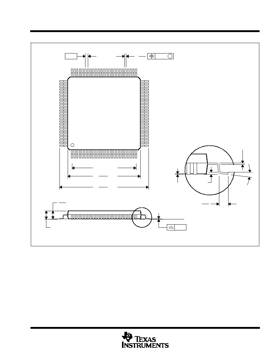
MECHANICAL DATA
MTQF013A ≠ OCTOBER 1994 ≠ REVISED DECEMBER 1996
1
POST OFFICE BOX 655303
∑
DALLAS, TEXAS 75265
PZ (S-PQFP-G100)
PLASTIC QUAD FLATPACK
4040149 /B 11/96
50
26
0,13 NOM
Gage Plane
0,25
0,45
0,75
0,05 MIN
0,27
51
25
75
1
12,00 TYP
0,17
76
100
SQ
SQ
15,80
16,20
13,80
1,35
1,45
1,60 MAX
14,20
0
∞
≠ 7
∞
Seating Plane
0,08
0,50
M
0,08
NOTES: A. All linear dimensions are in millimeters.
B. This drawing is subject to change without notice.
C. Falls within JEDEC MS-026

IMPORTANT NOTICE
Texas Instruments Incorporated and its subsidiaries (TI) reserve the right to make corrections, modifications,
enhancements, improvements, and other changes to its products and services at any time and to discontinue
any product or service without notice. Customers should obtain the latest relevant information before placing
orders and should verify that such information is current and complete. All products are sold subject to TI's terms
and conditions of sale supplied at the time of order acknowledgment.
TI warrants performance of its hardware products to the specifications applicable at the time of sale in
accordance with TI's standard warranty. Testing and other quality control techniques are used to the extent TI
deems necessary to support this warranty. Except where mandated by government requirements, testing of all
parameters of each product is not necessarily performed.
TI assumes no liability for applications assistance or customer product design. Customers are responsible for
their products and applications using TI components. To minimize the risks associated with customer products
and applications, customers should provide adequate design and operating safeguards.
TI does not warrant or represent that any license, either express or implied, is granted under any TI patent right,
copyright, mask work right, or other TI intellectual property right relating to any combination, machine, or process
in which TI products or services are used. Information published by TI regarding third-party products or services
does not constitute a license from TI to use such products or services or a warranty or endorsement thereof.
Use of such information may require a license from a third party under the patents or other intellectual property
of the third party, or a license from TI under the patents or other intellectual property of TI.
Reproduction of information in TI data books or data sheets is permissible only if reproduction is without
alteration and is accompanied by all associated warranties, conditions, limitations, and notices. Reproduction
of this information with alteration is an unfair and deceptive business practice. TI is not responsible or liable for
such altered documentation.
Resale of TI products or services with statements different from or beyond the parameters stated by TI for that
product or service voids all express and any implied warranties for the associated TI product or service and
is an unfair and deceptive business practice. TI is not responsible or liable for any such statements.
Following are URLs where you can obtain information on other Texas Instruments products and application
solutions:
Products
Applications
Amplifiers
amplifier.ti.com
Audio
www.ti.com/audio
Data Converters
dataconverter.ti.com
Automotive
www.ti.com/automotive
DSP
dsp.ti.com
Broadband
www.ti.com/broadband
Interface
interface.ti.com
Digital Control
www.ti.com/digitalcontrol
Logic
logic.ti.com
Military
www.ti.com/military
Power Mgmt
power.ti.com
Optical Networking
www.ti.com/opticalnetwork
Microcontrollers
microcontroller.ti.com
Security
www.ti.com/security
Telephony
www.ti.com/telephony
Video & Imaging
www.ti.com/video
Wireless
www.ti.com/wireless
Mailing Address:
Texas Instruments
Post Office Box 655303 Dallas, Texas 75265
Copyright 2006, Texas Instruments Incorporated