 | –≠–ª–µ–∫—Ç—Ä–æ–Ω–Ω—ã–π –∫–æ–º–ø–æ–Ω–µ–Ω—Ç: UN2003AI | –°–∫–∞—á–∞—Ç—å:  PDF PDF  ZIP ZIP |
www.ti.com
FEATURES
DESCRIPTION/ORDERING INFORMATION
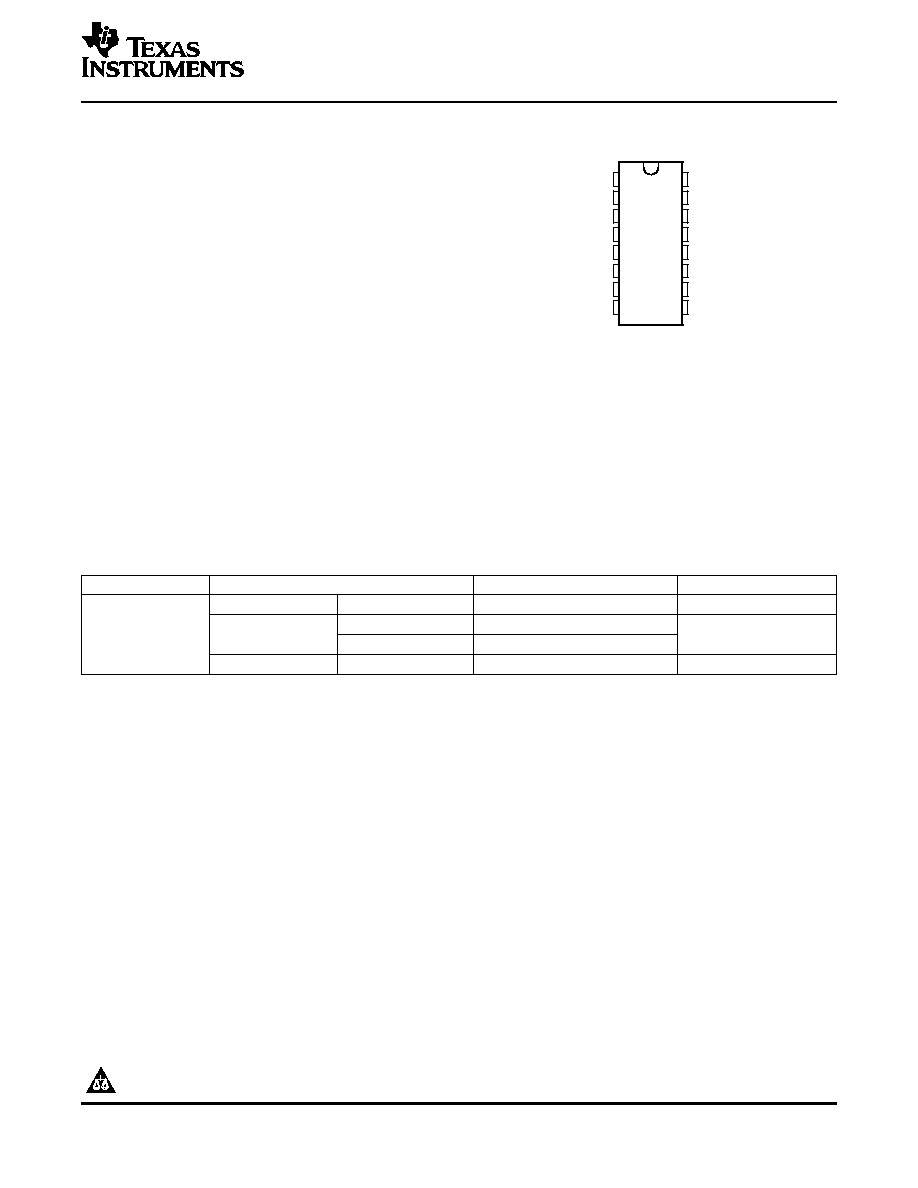
D, N, OR PW PACKAGE
(TOP VIEW)
1
2
3
4
5
6
7
8
16
15
14
13
12
11
10
9
1B
2B
3B
4B
5B
6B
7B
E
1C
2C
3C
4C
5C
6C
7C
COM
The ULN2003AI has a 2.7-k
series base resistor for each Darlington pair for operation directly with TTL or 5-V
ULN2003AI
HIGH-VOLTAGE, HIGH-CURRENT
DARLINGTON TRANSISTOR ARRAY
SLRS054B ≠ JULY 2003 ≠ REVISED FEBRUARY 2005
∑
500-mA-Rated Collector Current (Single
Output)
∑
High-Voltage Outputs . . . 50 V
∑
Output Clamp Diodes
∑
Inputs Compatible With Various Types of
Logic
∑
Relay-Driver Applications
The
ULN2003AI
is
a
high-voltage,
high-current
Darlington transistor array. This device consists of
seven npn Darlington pairs that feature high-voltage
outputs with common-cathode clamp diodes for
switching inductive loads. The collector-current rating
of a single Darlington pair is 500 mA. The Darlington
pairs can be paralleled for higher current capability.
Applications include relay drivers, hammer drivers,
lamp
drivers,
display
drivers
(LED
and
gas
discharge), line drivers, and logic buffers.
CMOS devices.
ORDERING INFORMATION
T
A
PACKAGE
ORDERABLE PART NUMBER
TOP-SIDE MARKING
PDIP (N)
Tube of 425
ULN2003AIN
ULN2003AIN
Tube of 40
ULN2003AID
≠40
∞
C to 105
∞
C
SOIC (D)
ULN2003AI
Reel of 2500
ULN2003AIDR
TSSOP (PW)
Reel of 2000
ULN2003AIPWR
UN2003AI
Please be aware that an important notice concerning availability, standard warranty, and use in critical applications of Texas
Instruments semiconductor products and disclaimers thereto appears at the end of this data sheet.
PRODUCTION DATA information is current as of publication date.
Copyright © 2003≠2005, Texas Instruments Incorporated
Products conform to specifications per the terms of the Texas
Instruments standard warranty. Production processing does not
necessarily include testing of all parameters.

www.ti.com
7C
6C
5C
4C
3C
2C
1C
COM
7
6
5
4
3
2
1
7B
6B
5B
4B
3B
2B
1B
10
11
12
13
14
15
16
9
Output
C
COM
E
7.2 k
3 k
2.7 k
Input
B
All resistor values shown are nominal.
ULN2003AI
HIGH-VOLTAGE, HIGH-CURRENT
DARLINGTON TRANSISTOR ARRAY
SLRS054B ≠ JULY 2003 ≠ REVISED FEBRUARY 2005
LOGIC DIAGRAM
SCHEMATICS (EACH DARLINGTON PAIR)
2
www.ti.com
Absolute Maximum Ratings
(1)
Electrical Characteristics
ULN2003AI
HIGH-VOLTAGE, HIGH-CURRENT
DARLINGTON TRANSISTOR ARRAY
SLRS054B ≠ JULY 2003 ≠ REVISED FEBRUARY 2005
at 25
∞
C free-air temperature (unless otherwise noted)
MIN
MAX
UNIT
V
CC
Collector-emitter voltage
50
V
Clamp diode reverse voltage
(2)
50
V
V
I
Input voltage
(2)
30
V
Peak collector current
(3) (4)
500
mA
I
OK
Output clamp current
500
mA
Total emitter-terminal current
≠2.5
A
T
A
Operating free-air temperature range
≠40
105
∞
C
D package
73
JA
Package thermal impedance
(3) (4)
N package
67
∞
C/W
PW package
108
T
J
Operating virtual junction temperature
150
∞
C
T
stg
Storage temperature range
≠65
150
∞
C
(1)
Stresses beyond those listed under "absolute maximum ratings" may cause permanent damage to the device. These are stress ratings
only, and functional operation of the device at these or any other conditions beyond those indicated under "recommended operating
conditions" is not implied. Exposure to absolute-maximum-rated conditions for extended periods may affect device reliability.
(2)
All voltage values are with respect to the emitter/substrate terminal E, unless otherwise noted.
(3)
Maximum power dissipation is a function of T
J
(max),
JA
, and T
A
. The maximum allowable power dissipation at any allowable ambient
temperature is P
D
= (T
J
(max) ≠ T
A
)/
JA
. Operating at the absolute maximum T
J
of 150
∞
C can affect reliability.
(4)
The package thermal impedance is calculated in accordance with JESD 51-7.
T
A
= 25
∞
C
PARAMETER
TEST FIGURE
TEST CONDITIONS
MIN
TYP
MAX
UNIT
I
C
= 200 mA
2.4
V
I(on)
On-state input voltage
5
V
CE
= 2 V
I
C
= 250 mA
2.7
V
I
C
= 300 mA
3
I
I
= 250
µ
A,
I
C
= 100 mA
0.9
1.1
V
CE(sat)
Collector-emitter saturation voltage
4
I
I
= 350
µ
A,
I
C
= 200 mA
1
1.3
V
I
I
= 500
µ
A,
I
C
= 350 mA
1.2
1.6
I
CEX
Collector cutoff current
1
V
CE
= 50 V,
I
I
= 0
50
µ
A
V
F
Clamp forward voltage
7
I
F
= 350 mA
1.7
2
V
I
I(off)
Off-state input current
2
V
CE
= 50 V,
I
C
= 500
µ
A
50
65
µ
A
I
I
Input current
3
V
I
= 3.85 V
0.93
1.35
mA
I
R
Clamp reverse current
6
V
R
= 50 V
50
µ
A
C
i
Input capacitance
V
I
= 0,
f = 1 MHz
15
25
pF
3
www.ti.com
Electrical Characteristics
Switching Characteristics
Switching Characteristics
ULN2003AI
HIGH-VOLTAGE, HIGH-CURRENT
DARLINGTON TRANSISTOR ARRAY
SLRS054B ≠ JULY 2003 ≠ REVISED FEBRUARY 2005
T
A
= ≠40
∞
C to 105
∞
C
PARAMETER
TEST FIGURE
TEST CONDITIONS
MIN
TYP
MAX
UNIT
I
C
= 200 mA
2.7
V
I(on)
On-state input voltage
5
V
CE
= 2 V
I
C
= 250 mA
2.9
V
I
C
= 300 mA
3
I
I
= 250
µ
A,
I
C
= 100 mA
0.9
1.2
V
CE(sat)
Collector-emitter saturation voltage
4
I
I
= 350
µ
A,
I
C
= 200 mA
1
1.4
V
I
I
= 500
µ
A,
I
C
= 350 mA
1.2
1.7
I
CEX
Collector cutoff current
1
V
CE
= 50 V,
I
I
= 0
100
µ
A
V
F
Clamp forward voltage
7
I
F
= 350 mA
1.7
2.2
V
I
I(off)
Off-state input current
2
V
CE
= 50 V,
I
C
= 500
µ
A
30
65
µ
A
I
I
Input current
3
V
I
= 3.85 V
0.93
1.35
mA
I
R
Clamp reverse current
6
V
R
= 50 V
100
µ
A
C
i
Input capacitance
V
I
= 0,
f = 1 MHz
15
25
pF
T
A
= 25
∞
C
PARAMETER
TEST CONDITIONS
MIN
TYP
MAX
UNIT
t
PLH
Propagation delay time, low- to high-level output
See Figure 8
0.25
1
µ
s
t
PHL
Propagation delay time, high- to low-level output
See Figure 8
0.25
1
µ
s
V
OH
High-level output voltage after switching
V
S
= 50 V,
I
O
300 mA, See Figure 9
V
S
≠ 20
mV
T
A
= ≠40
∞
C to 105
∞
C
PARAMETER
TEST CONDITIONS
MIN
TYP
MAX
UNIT
t
PLH
Propagation delay time, low- to high-level output
See Figure 8
1
10
µ
s
t
PHL
Propagation delay time, high- to low-level output
See Figure 8
1
10
µ
s
V
OH
High-level output voltage after switching
V
S
= 50 V,
I
O
300 mA, See Figure 9
V
S
≠ 50
mV
4
www.ti.com
PARAMETER MEASUREMENT INFORMATION
Open
V
CE
Open
I
CEX
Figure 1. I
CEX
Test Circuit
Open
V
CE
I
C
I
I(off)
Figure 2. I
I(off)
Test Circuit
Open
Open
I
I(on)
V
I
Figure 3. I
I
Test Circuit
Open
V
CE
I
C
I
I
h
FE
=
I
C
I
I
NOTE: I
I
is fixed for measuring V
CE(sat)
, variable for
measuring h
FE
.
Figure 4. h
FE
, V
CE(sat)
Test Circuit
Open
V
CE
I
C
V
I(on)
Figure 5. V
I(on)
Test Circuit
V
R
Open
I
R
Figure 6. I
R
Test Circuit
I
F
V
F
Open
Figure 7. V
F
Test Circuit
ULN2003AI
HIGH-VOLTAGE, HIGH-CURRENT
DARLINGTON TRANSISTOR ARRAY
SLRS054B ≠ JULY 2003 ≠ REVISED FEBRUARY 2005
5
www.ti.com
PARAMETER MEASUREMENT INFORMATION
50%
50%
50%
50%
t
PHL
VOLTAGE WAVEFORMS
Input
t
PLH
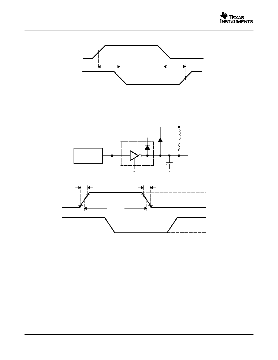
Figure 8. Propagation Delay-Time Waveforms
Output
Input
Open
V
S
200
Output
C
L
= 15 pF
(see Note B)
90%
90%
1.5 V
1.5 V
10%
10%
40
µ
s
10 ns
5 ns
V
IH
(see Note C)
0 V
V
OH
V
OL
Input
Output
TEST CIRCUIT
VOLTAGE WAVEFORMS
1N3064
2 mH
Pulse
Generator
(see Note A)
NOTES: A. The pulse generator has the following characteristics: PRR = 12.5 kHz, Z
O
= 50
.
B. C
L
includes probe and jig capacitance.
C. For testing, V
IH
= 3 V
Figure 9. Latch-Up Test Circuit and Voltage Waveforms
ULN2003AI
HIGH-VOLTAGE, HIGH-CURRENT
DARLINGTON TRANSISTOR ARRAY
SLRS054B ≠ JULY 2003 ≠ REVISED FEBRUARY 2005
6

www.ti.com
TYPICAL CHARACTERISTICS
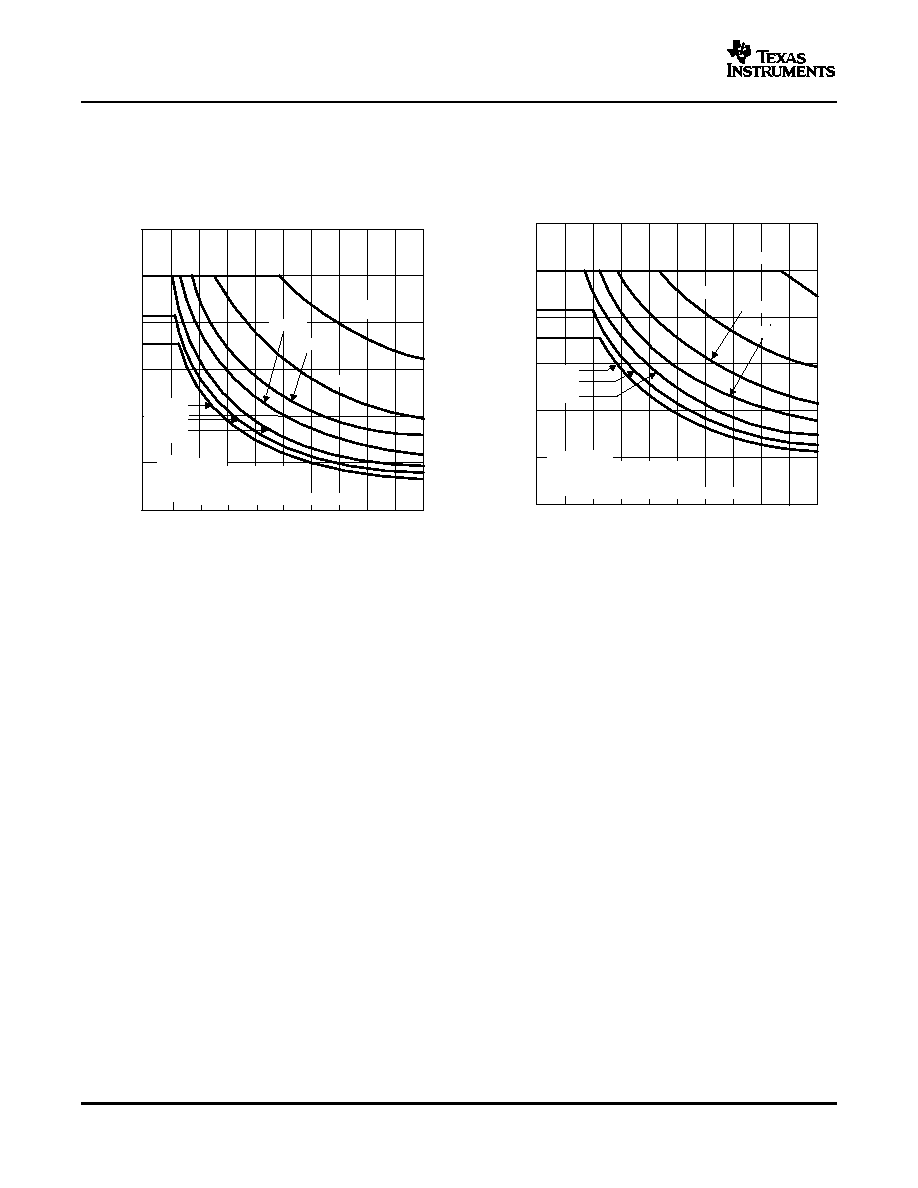
Figure 10
COLLECTOR-EMITTER
SATURATION VOLTAGE
vs
COLLECTOR CURRENT
(ONE DARLINGTON)
0
I
C
- Collector Current - mA
2.5
800
0
100
200
300
400
500
600
700
0.5
1
1.5
2
I
I
= 350
µ
A
I
I
= 500
µ
A
VCE(sat) - Collector-Emitter Saturation V
oltage - V
V
CE(sat)
T
A
= 25
∞
C
I
I
= 250
µ
A
2
1.5
1
0.5
700
600
500
400
300
200
100
0
800
2.5
I
C(tot)
- Total Collector Current - mA
0
COLLECTOR-EMITTER
SATURATION VOLTAGE
vs
TOTAL COLLECTOR CURRENT
(TWO DARLINGTONS IN PARALLEL)
VCE(sat) - Collector-Emitter Saturation V
oltage - V
V
CE(sat)
I
I
= 250
µ
A
I
I
= 350
µ
A
I
I
= 500
µ
A
T
A
= 25
∞
C
COLLECTOR CURRENT
vs
INPUT CURRENT
0
I
I
- Input Current -
µ
A
500
200
0
25
50
75
100
125
150
175
50
100
150
200
250
300
350
400
450
V
S
= 10 V
V
S
= 8 V
IC - Collector Current - mA CI
R
L
= 10
T
A
= 25
∞
C
Figure 12
Figure 11
ULN2003AI
HIGH-VOLTAGE, HIGH-CURRENT
DARLINGTON TRANSISTOR ARRAY
SLRS054B ≠ JULY 2003 ≠ REVISED FEBRUARY 2005
7
www.ti.com
THERMAL INFORMATION
Figure 13
0
Duty Cycle - %
600
100
0
10
20
30
40
50
60
70
80
90
100
200
300
400
500
T
A
= 70
∞
C
N = Number of Outputs
Conducting Simultaneously
N = 7
N = 6
D PACKAGE
MAXIMUM COLLECTOR CURRENT
vs
DUTY CYCLE
N = 5
N = 3
N = 2
N = 1
IC - Maximum Collector Current - mA CI
N = 4
Figure 14
Conducting Simultaneously
N = Number of Outputs
500
400
300
200
100
90
80
70
60
50
40
30
20
10
0
100
600
Duty Cycle - %
0
N = 5
T
A
= 85
∞
C
N PACKAGE
MAXIMUM COLLECTOR CURRENT
vs
DUTY CYCLE
N = 7
N = 3
N = 2
N = 6
N = 1
IC - Maximum Collector Current - mA CI
N = 4
ULN2003AI
HIGH-VOLTAGE, HIGH-CURRENT
DARLINGTON TRANSISTOR ARRAY
SLRS054B ≠ JULY 2003 ≠ REVISED FEBRUARY 2005
8

www.ti.com
APPLICATION INFORMATION
Lamp
Test
TTL
Output
V
CC
V
1
2
3
4
5
6
9
10
11
12
13
14
15
16
8
7
Figure 15. TTL to Load
V
CC
V
R
P
1
2
3
4
5
6
9
10
11
12
13
14
15
16
8
TTL
Output
7
Figure 16. Use of Pullup Resistors
to Increase Drive Current
ULN2003AI
HIGH-VOLTAGE, HIGH-CURRENT
DARLINGTON TRANSISTOR ARRAY
SLRS054B ≠ JULY 2003 ≠ REVISED FEBRUARY 2005
9
PACKAGING INFORMATION
Orderable Device
Status
(1)
Package
Type
Package
Drawing
Pins Package
Qty
Eco Plan
(2)
Lead/Ball Finish
MSL Peak Temp
(3)
ULN2003AID
ACTIVE
SOIC
D
16
40
Pb-Free
(RoHS)
CU NIPDAU
Level-2-260C-1 YEAR/
Level-1-235C-UNLIM
ULN2003AIDR
ACTIVE
SOIC
D
16
2500
Pb-Free
(RoHS)
CU NIPDAU
Level-2-260C-1 YEAR/
Level-1-235C-UNLIM
ULN2003AIN
ACTIVE
PDIP
N
16
25
Pb-Free
(RoHS)
CU NIPDAU
Level-NC-NC-NC
ULN2003AIPW
ACTIVE
TSSOP
PW
16
90
Pb-Free
(RoHS)
CU NIPDAU
Level-1-250C-UNLIM
ULN2003AIPWR
ACTIVE
TSSOP
PW
16
2000
Pb-Free
(RoHS)
CU NIPDAU
Level-1-250C-UNLIM
(1)
The marketing status values are defined as follows:
ACTIVE: Product device recommended for new designs.
LIFEBUY: TI has announced that the device will be discontinued, and a lifetime-buy period is in effect.
NRND: Not recommended for new designs. Device is in production to support existing customers, but TI does not recommend using this part in
a new design.
PREVIEW: Device has been announced but is not in production. Samples may or may not be available.
OBSOLETE: TI has discontinued the production of the device.
(2)
Eco Plan - May not be currently available - please check
http://www.ti.com/productcontent
for the latest availability information and additional
product content details.
None: Not yet available Lead (Pb-Free).
Pb-Free (RoHS): TI's terms "Lead-Free" or "Pb-Free" mean semiconductor products that are compatible with the current RoHS requirements
for all 6 substances, including the requirement that lead not exceed 0.1% by weight in homogeneous materials. Where designed to be soldered
at high temperatures, TI Pb-Free products are suitable for use in specified lead-free processes.
Green (RoHS & no Sb/Br): TI defines "Green" to mean "Pb-Free" and in addition, uses package materials that do not contain halogens,
including bromine (Br) or antimony (Sb) above 0.1% of total product weight.
(3)
MSL, Peak Temp. -- The Moisture Sensitivity Level rating according to the JEDECindustry standard classifications, and peak solder
temperature.
Important Information and Disclaimer:The information provided on this page represents TI's knowledge and belief as of the date that it is
provided. TI bases its knowledge and belief on information provided by third parties, and makes no representation or warranty as to the
accuracy of such information. Efforts are underway to better integrate information from third parties. TI has taken and continues to take
reasonable steps to provide representative and accurate information but may not have conducted destructive testing or chemical analysis on
incoming materials and chemicals. TI and TI suppliers consider certain information to be proprietary, and thus CAS numbers and other limited
information may not be available for release.
In no event shall TI's liability arising out of such information exceed the total purchase price of the TI part(s) at issue in this document sold by TI
to Customer on an annual basis.
PACKAGE OPTION ADDENDUM
www.ti.com
28-Feb-2005
Addendum-Page 1
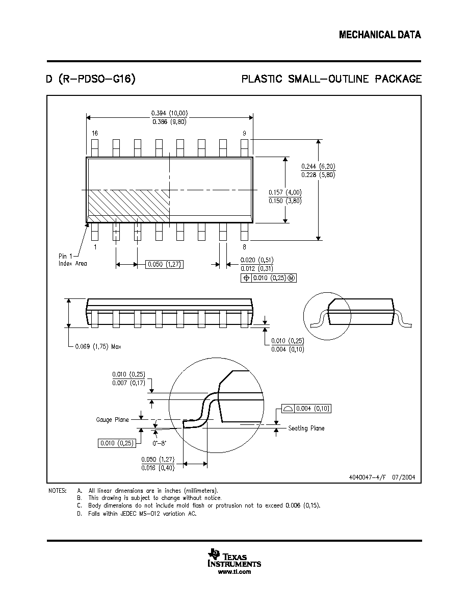
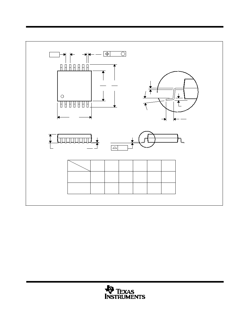
MECHANICAL DATA
MTSS001C ≠ JANUARY 1995 ≠ REVISED FEBRUARY 1999
POST OFFICE BOX 655303
∑
DALLAS, TEXAS 75265
PW (R-PDSO-G**)
PLASTIC SMALL-OUTLINE PACKAGE
14 PINS SHOWN
0,65
M
0,10
0,10
0,25
0,50
0,75
0,15 NOM
Gage Plane
28
9,80
9,60
24
7,90
7,70
20
16
6,60
6,40
4040064/F 01/97
0,30
6,60
6,20
8
0,19
4,30
4,50
7
0,15
14
A
1
1,20 MAX
14
5,10
4,90
8
3,10
2,90
A MAX
A MIN
DIM
PINS **
0,05
4,90
5,10
Seating Plane
0
∞
≠ 8
∞
NOTES: A. All linear dimensions are in millimeters.
B. This drawing is subject to change without notice.
C. Body dimensions do not include mold flash or protrusion not to exceed 0,15.
D. Falls within JEDEC MO-153

IMPORTANT NOTICE
Texas Instruments Incorporated and its subsidiaries (TI) reserve the right to make corrections, modifications,
enhancements, improvements, and other changes to its products and services at any time and to discontinue
any product or service without notice. Customers should obtain the latest relevant information before placing
orders and should verify that such information is current and complete. All products are sold subject to TI's terms
and conditions of sale supplied at the time of order acknowledgment.
TI warrants performance of its hardware products to the specifications applicable at the time of sale in
accordance with TI's standard warranty. Testing and other quality control techniques are used to the extent TI
deems necessary to support this warranty. Except where mandated by government requirements, testing of all
parameters of each product is not necessarily performed.
TI assumes no liability for applications assistance or customer product design. Customers are responsible for
their products and applications using TI components. To minimize the risks associated with customer products
and applications, customers should provide adequate design and operating safeguards.
TI does not warrant or represent that any license, either express or implied, is granted under any TI patent right,
copyright, mask work right, or other TI intellectual property right relating to any combination, machine, or process
in which TI products or services are used. Information published by TI regarding third-party products or services
does not constitute a license from TI to use such products or services or a warranty or endorsement thereof.
Use of such information may require a license from a third party under the patents or other intellectual property
of the third party, or a license from TI under the patents or other intellectual property of TI.
Reproduction of information in TI data books or data sheets is permissible only if reproduction is without
alteration and is accompanied by all associated warranties, conditions, limitations, and notices. Reproduction
of this information with alteration is an unfair and deceptive business practice. TI is not responsible or liable for
such altered documentation.
Resale of TI products or services with statements different from or beyond the parameters stated by TI for that
product or service voids all express and any implied warranties for the associated TI product or service and
is an unfair and deceptive business practice. TI is not responsible or liable for any such statements.
Following are URLs where you can obtain information on other Texas Instruments products and application
solutions:
Products
Applications
Amplifiers
amplifier.ti.com
Audio
www.ti.com/audio
Data Converters
dataconverter.ti.com
Automotive
www.ti.com/automotive
DSP
dsp.ti.com
Broadband
www.ti.com/broadband
Interface
interface.ti.com
Digital Control
www.ti.com/digitalcontrol
Logic
logic.ti.com
Military
www.ti.com/military
Power Mgmt
power.ti.com
Optical Networking
www.ti.com/opticalnetwork
Microcontrollers
microcontroller.ti.com
Security
www.ti.com/security
Telephony
www.ti.com/telephony
Video & Imaging
www.ti.com/video
Wireless
www.ti.com/wireless
Mailing Address:
Texas Instruments
Post Office Box 655303 Dallas, Texas 75265
Copyright
2005, Texas Instruments Incorporated