Document Outline
- FEATURES
- DESCRIPTION
- APPLICATIONS
- ABSOLUTE MAXIMUM RATINGS(
- PACKAGE/ORDERING INFORMATION
- ELECTRICAL CHARACTERISTICS
- PIN CONFIGURATION
- PIN DESCRIPTIONS
- TYPICAL CHARACTERISTICS
- THEORY OF OPERATION
- LNP - OVERVIEW
- VCA - OVERVIEW
- PGA OVERVIEW AND OVERALL DEVICE CHARACTERISTICS
- ADDITIONAL FEATURES - OVERVIEW
- LOW-NOISE PREAMPLIFIER (LNP) - DETAIL
- ACTIVE FEEDBACK WITH THE LNP
- COMPENSATION WHEN USING ACTIVE FEEDBACK
- AVOIDING UNSTABLE PERFORMANCE
- LNP OUTPUT BUFFER
- VOLTAGE-CONTROLLED ATTENUATOR (VCA) - DETAIL
- INPUT OVERLOAD RECOVERY
- PGA POST-AMPLIFIER - DETAIL

FEATURES
q
LOW-NOISE PREAMP:
≠ Low Input Noise: 0.95nV/
Hz
≠ Active Termination Noise Reduction
≠ Switchable Termination Value
≠ 80MHz Bandwidth
≠ 5dB to 25dB Gain
≠ Differential In and Out
q
LOW-NOISE VARIABLE GAIN AMPLIFIER:
≠ Low-Noise VCA
≠ Up to 40dB Gain Range
≠ 40MHz Bandwidth
≠ Differential In and Out
q
LOW CROSSTALK: 66dB at Max Gain, 5MHz
q
HIGH-SPEED VARIABLE GAIN ADJUST
q
SWITCHABLE EXTERNAL PROCESSING
APPLICATIONS
q
ULTRASOUND SYSTEMS
q
WIRELESS RECEIVERS
q
TEST EQUIPMENT
DESCRIPTION
The VCA2616 and VCA2611 are dual, Low-Noise Preamplifiers
(LNP), plus low-noise Variable Gain Amplifiers (VGA). The
VCA2611 is an upgraded version of the VCA2616. The only
difference between the VCA2616 and the VCA2611 is the input
structure to the LNP. The VCA2616 is limited to ≠0.3V negative-
going input spikes; the VCA2611 is limited to ≠2.0V negative-
going input spikes. This change allows the user to use slower
and less expensive input clamping diodes prior to the LNP input.
In some designs, input clamping may not be required.
The combination of Active Termination (AT) and Maximum
Gain Select (MGS) allow for the best noise performance. The
VCA2616 and VCA2611 also feature low crosstalk and out-
standing distortion performance.
The LNP has differential input and output capability and is
strappable for gains of 5dB, 17dB, 22dB, or 25dB. Low input
impedance is achieved by AT, resulting in as much as a 4.6dB
improvement in noise figure over conventional shunt termina-
tion. The termination value can also be switched to accommo-
date different sources. The output of the LNP is available for
external signal processing.
The variable gain is controlled by an analog voltage whose
gain varies from 0dB to the gain set by the MGS. The ability
to program the variable gain also allows the user to optimize
dynamic range. The VCA input can be switched from the LNP
to external circuits for different applications. The output can be
used in either a single-ended or differential mode to drive high-
performance Analog-to-Digital (A/D) converters, and is cleanly
limited for optimum overdrive recovery.
The combination of low noise, gain, and gain range program-
mability makes the VCA2616 and VCA2611 versatile building
blocks in a number of applications where noise performance
is critical. The VCA2616 and VCA2611 are available in a
TQFP-48 package.
Dual, Variable-Gain Amplifier
with Low-Noise Preamp
Low Noise
Preamp
5dB to 25dB
Programmable
Gain Amplifier
24 to 45dB
Voltage
Controlled
Attenuator
Analog
Control
Maximum Gain
Select
RF
2
RF
1
FB
FBSW
LNP
IN
P
LNP
IN
N
LNP
GS1
LNP
GS2
LNP
GS3
LNP
Gain
Set
Input
LNP
OUT
P
SEL
VCA
IN
P
LNP
OUT
N VCA
IN
N
VCA
CNTL
FB
CNTL
VCA
OUT
P
VCA
OUT
N
MGS
1
MGS
2
MGS
3
Maximum Gain Select
VCA2616
(1 of 2 Channels)
VCA2616
VCA2611
SBOS234C ≠ MARCH 2002 ≠ REVISED SEPTEMBER 2003
VCA2
616
www.ti.com
Copyright © 2002-2003, Texas Instruments Incorporated
All trademarks are the property of their respective owners.
Please be aware that an important notice concerning availability, standard warranty, and use in critical applications of
Texas Instruments semiconductor products and disclaimers thereto appears at the end of this data sheet.
PRODUCTION DATA information is current as of publication date.
Products conform to specifications per the terms of Texas Instruments
standard warranty. Production processing does not necessarily include
testing of all parameters.
VCA2616, VCA2611
2
SBOS234C
www.ti.com
ABSOLUTE MAXIMUM RATINGS
(1)
SPECIFIED
PACKAGE
TEMPERATURE
PACKAGE
ORDERING
TRANSPORT
PRODUCT
PACKAGE-LEAD
DESIGNATOR
(1)
RANGE
MARKING
NUMBER
MEDIA, QUANTITY
VCA2616
TQFP-48
PFB
≠40
∞
C to +85
∞
C
VCA2616
VCA2616YT
Tape and Reel, 250
"
"
"
"
"
VCA2616YR
Tape and Reel, 2000
VCA2611
TQFP-48
PFB
≠40
∞
C to +85
∞
C
VCA2611
VCA2611Y/250
Tape and Reel, 250
"
"
"
"
"
VCA2611Y/2K
Tape and Reel, 2000
NOTE: (1) For the most current specifications, and package information, refer to our web site at www.ti.com.
PACKAGE/ORDERING INFORMATION
ELECTRICAL CHARACTERISTICS
At T
A
= +25
∞
C, V
DDA
= V
DDB
= V
DDR
= +5V, load resistance = 500
on each output to ground, MGS = 011, LNP = 22dB and f
IN
= 5MHz, unless otherwise noted.
The input to the preamp (LNP) is single-ended, and the output from the VCA is single-ended, unless otherwise noted.
VCA2616Y, VCA2611Y
PARAMETER
CONDITIONS
MIN
TYP
MAX
UNITS
PREAMPLIFIER
Input Resistance
600
k
Input Capacitance
15
pF
Input Bias Current
1
nA
CMRR
f = 1MHz, VCA
CNTL
= 0.2V
50
dB
Maximum Input Voltage
Preamp Gain = +5dB
1
V
PP
Preamp Gain = +25dB
112
mV
PP
Input Voltage Noise
(1)
Preamp Gain = +5dB
4.2
nV/
Hz
Preamp Gain = +25dB
0.95
nV/
Hz
Input Current Noise
Independent of Gain
0.35
pA/
Hz
Noise Figure, R
S
= 75
, R
IN
= 75
(1)
R
F
= 550
, Preamp Gain = 22dB,
6.2
dB
PGA Gain = 39dB
Bandwidth
Gain = 22dB
80
MHz
PROGRAMMABLE VARIABLE GAIN AMPLIFIER
Peak Input Voltage
Differential
2
V
PP
≠3dB Bandwidth
40
MHz
Slew Rate
300
V/
µ
s
Output Signal Range
R
L
500
Each Side to Ground
2
V
PP
Output Impedance
f = 5MHz
1
Output Short-Circuit Current
±
40
mA
3rd-Harmonic Distortion
f = 5MHz, V
OUT
= 1V
PP
, VCA
CNTL
= 3.0V
≠45
≠71
dBc
2nd-Harmonic Distortion
f = 5MHz, V
OUT
= 1V
PP
, VCA
CNTL
= 3.0V
≠45
≠63
dBc
IMD, 2-Tone
V
OUT
= 2V
PP
, f = 1MHz
≠75
dBc
V
OUT
= 2V
PP
, f = 10MHz
≠75
dBc
Crosstalk
VCA
CNTL
= 0.2V
≠66
dB
Group Delay Variation
1MHz < f < 10MHz, Full Gain Range
±
2
ns
DC Output Level, V
IN
= 0
2.5
V
ACCURACY
Gain Slope
10.9
dB/V
Gain Error
±
1
(2)
dB
Output Offset Voltage
±
50
mV
GAIN CONTROL INTERFACE
Input Voltage (VCA
CNTL
) Range
0.2 to 3.0
V
Input Resistance
1
M
Response Time
40dB Gain Change, MGS = 111
0.2
µ
s
POWER SUPPLY
Operating Temperature Range
≠40
+85
∞
C
Specified Operating Range
4.75
5.0
5.25
V
Power Dissipation
Operating, Both Channels
410
495
mW
ELECTROSTATIC
DISCHARGE SENSITIVITY
This integrated circuit can be damaged by ESD. Texas Instru-
ments recommends that all integrated circuits be handled with
appropriate precautions. Failure to observe proper handling
and installation procedures can cause damage.
ESD damage can range from subtle performance degrada-
tion to complete device failure. Precision integrated circuits
may be more susceptible to damage because very small
parametric changes could cause the device not to meet its
published specifications.
Power Supply (+V
S
) ............................................................................. +6V
VCA2616 Analog Input ............................................ ≠0.3V to (+V
S
+ 0.3V)
VCA2611 Analog Input ............................................ ≠2.0V to (+V
S
+ 0.3V)
Logic Input ............................................................... ≠0.3V to (+V
S
+ 0.3V)
Case Temperature ......................................................................... +100
∞
C
Junction Temperature .................................................................... +150
∞
C
Storage Temperature ...................................................... ≠40
∞
C to +150
∞
C
NOTE: (1) Stresses above those listed under "Absolute Maximum Ratings" may
cause permanent damage to the device. Exposure to absolute maximum
conditions for extended periods may affect device reliability.
(1) For preamp driving VGA.
(2) Referenced to best fit dB-linear curve.
VCA2616, VCA2611
3
SBOS234C
www.ti.com
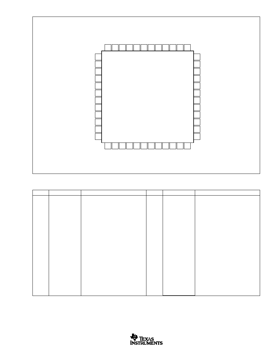
PIN CONFIGURATION
36
35
34
33
32
31
30
29
28
27
26
25
V
DD
B
NC
NC
VCA
IN
NB
VCA
IN
PB
LNP
OUT
NB
LNP
OUT
PB
SWFBB
FBB
COMP1B
COMP2B
LNP
IN
NB
GNDA
VCA
OUT
NA
VCA
OUT
PA
FBSW
CNTL
VCA
IN
SEL
VCA
CNTL
MGS
1
MGS
2
MGS
3
VCA
OUT
PB
VCA
OUT
NB
GNDB
LNP
GS3
A
LNP
GS2
A
LNP
GS1
A
LNP
IN
PA
V
DD
R
V
BIAS
V
CM
GNDR
LNP
IN
PB
LNP
GS1
B
LNP
GS2
B
LNP
GS3
B
1
2
3
4
5
6
7
8
9
10
11
12
V
DD
A
NC
NC
VCA
IN
NA
VCA
IN
PA
LNP
OUT
NA
LNP
OUT
PA
SWFBA
FBA
COMP1A
COMP2A
LNP
IN
NA
48
47
46
45
44
43
42
41
40
39
38
13
14
15
16
17
18
19
20
21
22
23
37
24
VCA2616
VCA2611
1
V
DD
A
Channel A +Supply
2
NC
Do Not Connect
3
NC
Do Not Connect
4
VCA
IN
NA
Channel A VCA Negative Input
5
VCA
IN
PA
Channel A VCA Positive Input
6
LNP
OUT
NA
Channel A LNP Negative Output
7
LNP
OUT
PA
Channel A LNP Positive Output
8
SWFBA
Channel A Switched Feedback Output
9
FBA
Channel A Feedback Output
10
COMP1A
Channel A Frequency Compensation 1
11
COMP2A
Channel A Frequency Compensation 2
12
LNP
IN
NA
Channel A LNP Inverting Input
13
LNP
GS3
A
Channel A LNP Gain Strap 3
14
LNP
GS2
A
Channel A LNP Gain Strap 2
15
LNP
GS1
A
Channel A LNP Gain Strap 1
16
LNP
IN
PA
Channel A LNP Noninverting Input
17
V
DD
R
+Supply for Internal Reference
18
V
BIAS
0.01
µ
F Bypass to Ground
19
V
CM
0.01
µ
F Bypass to Ground
20
GNDR
Ground for Internal Reference
21
LNP
IN
PB
Channel B LNP Noninverting Input
22
LNP
GS1
B
Channel B LNP Gain Strap 1
23
LNP
GS2
B
Channel B LNP Gain Strap 2
24
LNP
GS3
B
Channel B LNP Gain Strap 3
25
LNP
IN
NB
Channel B LNP Inverting Input
26
COMP2B
Channel B Frequency Compensation 2
27
COMP1B
Channel B Frequency Compensation 1
28
FBB
Channel B Feedback Output
29
SWFBB
Channel B Switched Feedback Output
30
LNP
OUT
PB
Channel B LNP Positive Output
31
LNP
OUT
NB
Channel B LNP Negative Output
32
VCA
IN
PB
Channel B VCA Positive Input
33
VCA
IN
NB
Channel B VCA Negative Input
34
NC
Do Not Connect
35
NC
Do Not Connect
36
V
DD
B
Channel B +Analog Supply
37
GNDB
Channel B Analog Ground
38
VCA
OUT
NB
Channel B VCA Negative Output
39
VCA
OUT
PB
Channel B VCA Positive Output
40
MGS
3
Maximum Gain Select 3 (LSB)
41
MGS
2
Maximum Gain Select 2
42
MGS
1
Maximum Gain Select 1 (MSB)
43
VCA
CNTL
VCA Control Voltage
44
VCA
IN
SEL
VCA Input Select, HI = External
45
FBSW
CNTL
Feedback Switch Control: HI = ON
46
VCA
OUT
PA
Channel A VCA Positive Output
47
VCA
OUT
NA
Channel A VCA Negative Output
48
GNDA
Channel A Analog Ground
PIN
DESIGNATOR
DESCRIPTION
PIN
DESIGNATOR
DESCRIPTION
PIN DESCRIPTIONS
Top View
TQFP
VCA2616, VCA2611
4
SBOS234C
www.ti.com
TYPICAL CHARACTERISTICS
At T
A
= +25
∞
C, V
DDA
= V
DDB
= V
DDR
= +5V, load resistance = 500
on each output to ground, MGS = 011, LNP = 22dB and f
IN
= 5MHz, unless otherwise noted.
The input to the preamp (LNP) is single-ended, and the output from the VCA is single-ended, unless otherwise noted. This results in a 6dB reduction in signal
amplitude compared to differential operation.
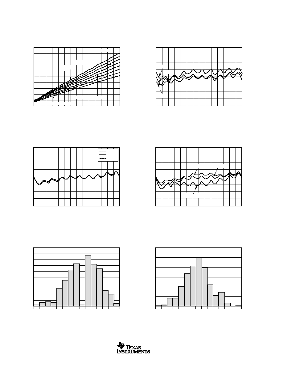
GAIN vs VCA
CNTL
VCA
CNTL
(V)
0.2
1.2
1.0
0.4 0.6 0.8
1.8 2.0 2.2
1.6
1.4
2.4 2.6 2.8 3.0
Gain (dB)
65
60
55
50
45
40
35
30
25
20
15
MGS = 110
MGS = 111
MGS = 101 MGS = 100
MGS = 011
MGS = 010
MGS = 001
MGS = 000
GAIN ERROR vs TEMPERATURE
VCA
CNTL
(V)
0.2
1.0 1.2
0.8
0.4 0.6
2.0 2.2
1.4 1.6 1.8
2.4 2.6 2.8 3.0
Gain Error (dB)
2.0
1.5
1.0
0.5
0.0
≠0.5
≠1.0
≠1.5
≠2.0
+85
∞
C
≠40
∞
C
+25
∞
C
GAIN ERROR vs VCA
CNTL
VCA
CNTL
(V)
0.2
1.0 1.2
0.8
0.4 0.6
2.0 2.2
1.4 1.6 1.8
2.4 2.6 2.8 3.0
Gain Error (dB)
2.0
1.5
1.0
0.5
0.0
≠0.5
≠1.0
≠1.5
≠2.0
10MHz
1MHz
5MHz
GAIN ERROR vs VCA
CNTL
VCA
CNTL
(V)
0.2
1.0 1.2
0.8
0.4 0.6
2.0 2.2
1.4 1.6 1.8
2.4 2.6 2.8 3.0
Gain Error (dB)
2.0
1.5
1.0
0.5
0
≠0.5
≠1.0
≠1.5
≠2.0
MGS = 011
MGS = 000
MGS = 111
GAIN MATCH
0.2V CHA to CHB
Delta Gain (dB)
Units
50
45
40
35
30
25
20
15
10
5
0
≠
0.55
≠
0.48
≠
0.42
≠
0.35
≠
0.29
≠
0.22
≠
0.16
≠
0.09
≠
0.03
0.04
0.16
0.10
0.23
0.36
0.29
Delta Gain (dB)
≠
0.26
≠
0.23
≠
0.20
≠
0.17
≠
0.14
≠
0.10
0.07
0.04
0.01
0.02
0.09
0.05
0.12
0.18
0.15
Units
60
50
40
30
20
10
0
GAIN MATCH
3.0V CHA to CHB
VCA2616, VCA2611
5
SBOS234C
www.ti.com
TYPICAL CHARACTERISTICS
(Cont.)
At T
A
= +25
∞
C, V
DDA
= V
DDB
= V
DDR
= +5V, load resistance = 500
on each output to ground, MGS = 011, LNP = 22dB and f
IN
= 5MHz, unless otherwise noted.
The input to the preamp (LNP) is single-ended, and the output from the VCA is single-ended, unless otherwise noted. This results in a 6dB reduction in signal
amplitude compared to differential operation.
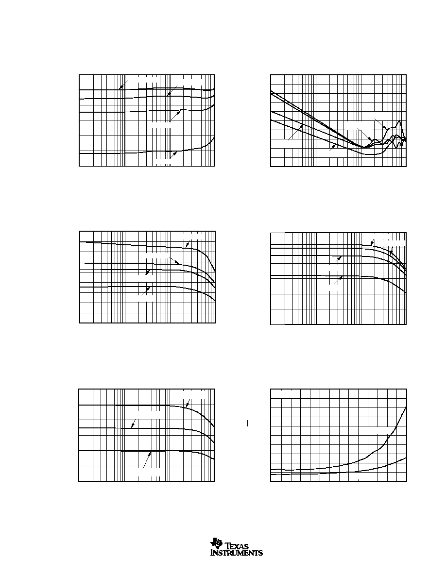
GAIN vs FREQUENCY
(Pre-Amp)
Frequency (Hz)
Gain (dB)
30
25
20
15
10
5
0
LNA = 25dB
LNA = 22dB
LNA = 17dB
LNA = 5dB
100k
1M
10M
100M
GAIN vs FREQUENCY
VCA
(VCA
CNTL
= 0.2V)
Frequency (Hz)
Gain (dB)
5.0
4.0
3.0
2.0
1.0
0.0
≠1.0
≠2.0
≠3.0
≠4.0
≠5.0
MGS = 111
MGS = 100
MGS = 011
MGS = 000
100k
1M
10M
100M
GAIN vs FREQUENCY
VCA
(VCA
CNTL
= 3.0V)
Frequency (Hz)
Gain (dB)
45
40
35
30
25
20
15
10
5
0
MGS = 111
MGS = 100
MGS = 011
MGS = 000
100k
1M
10M
100M
GAIN vs FREQUENCY
LNA and VCA
(VCA
CNTL
= 3.0V)
Frequency (Hz)
100k
1M
10M
100M
Gain (dB)
60
50
40
30
20
10
0
LNP = 25dB
LNP = 22dB
LNP = 5dB
LNP = 17dB
GAIN vs FREQUENCY
LNA and VCA
(LNP = 22dB)
Frequency (Hz)
Gain (dB)
60
50
40
30
20
10
0
V
CNTL
= 3.0V
V
CNTL
= 1.6V
V
CNTL
= 0.2V
100k
1M
10M
100M
OUTPUT-REFERRED NOISE vs VCA
CNTL
(LNP = 25dB)
VCA
CNTL
(V)
0.2
1.0 1.2
0.4 0.6 0.8
1.8 2.0
1.4 1.6
2.2 2.4 2.6 2.8 3.0
Noise (nV/
Hz)
2000
1800
1600
1400
1200
1000
800
600
400
200
0
R
S
= 50
MGS = 111
MGS = 011