 | –≠–ª–µ–∫—Ç—Ä–æ–Ω–Ω—ã–π –∫–æ–º–ø–æ–Ω–µ–Ω—Ç: VCA8613 | –°–∫–∞—á–∞—Ç—å:  PDF PDF  ZIP ZIP |
8-Channel
VARIABLE GAIN AMPLIFIER
FEATURES
q
3V OPERATION
q
LOW INPUT NOISE: 1.2nV
Hz at f
IN
= 5MHz
q
EXTREMELY LOW POWER OPERATION:
75mW/CHANNEL
q
INTEGRATED LOW-PASS, 2-POLE FILTER
14MHz BANDWIDTH
VCA8613
SBOS200C ≠ APRIL 2003 ≠ REVISED MARCH 2004
www.ti.com
Copyright © 2003-2004, Texas Instruments Incorporated
OutP
(1)
OutN
(1)
LNAIN1
LNA
V
LNA
V
LNA
Attenuator
Analog
Control
PGA
2-Pole
Filter
CW
(1-10)
D
(0-3)
CW Processor
5x8
FIFO
OutP
(8)
OutN
(8)
LNAIN8
LNA
Attenuator
PGA
2-Pole
Filter
∑
∑
∑
∑
∑
∑
DATA
CLK
CS
Serial
Interface
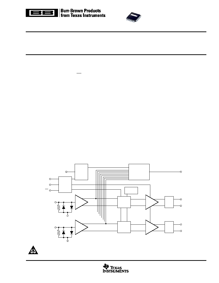
DESCRIPTION
The VCA8613 is an 8-channel variable gain amplifier ideally
suited to portable ultrasound applications. Excellent dynamic
performance enables use in low-power, high-performance
portable applications. Each channel consists of a Low-Noise
pre-Amplifier (LNA) and a Variable Gain Amplifier (VGA). The
differential outputs of the LNA can be switched through the
8x10 cross-point switch, which is programmable through the
serial interface input port.
The output of the LNA is fed directly into the VGA stage. The
VGA consists of two parts, a Voltage Controlled Attenuator
(VCA) and a Programmable Gain Amplifier (PGA). The gain and
q
INTEGRATED INPUT CLAMP DIODES
q
DIFFERENTIAL OUTPUT
q
INTEGRATED INPUT LNA
q
READABLE CONTROL REGISTERS
q
INTEGRATED CONTINUOUS WAVE (CW)
PROCESSOR
gain range of the PGA can be digitally configured separately. The
gain of the PGA can be varied between two discrete settings of
21dB and 26dB. The VCA has four programmable maximum
attenuation settings: 29dB, 33dB, 36.5dB, and 40dB. Also, the
VCA can be continuously varied by a control voltage from 0dB to
a maximum of 29dB, 33dB, 36.5dB, and 40dB.
The output of the PGA feeds directly into an integrated
2-pole, low-pass filter, allowing for direct connection to a
differential input Analog-to-Digital Converter (ADC), such as
the ADS5121 or ADS5122 from Texas Instruments. The
VCA8613 is available in a TQFP-64 package.
Please be aware that an important notice concerning availability, standard warranty, and use in critical applications of
Texas Instruments semiconductor products and disclaimers thereto appears at the end of this data sheet.
All trademarks are the property of their respective owners.
VCA8613
Æ
PRODUCTION DATA information is current as of publication date.
Products conform to specifications per the terms of Texas Instruments
standard warranty. Production processing does not necessarily include
testing of all parameters.

VCA8613
2
SBOS200C
www.ti.com
ELECTROSTATIC
DISCHARGE SENSITIVITY
This integrated circuit can be damaged by ESD. Texas Instru-
ments recommends that all integrated circuits be handled with
appropriate precautions. Failure to observe proper handling
and installation procedures can cause damage.
ESD damage can range from subtle performance degradation
to complete device failure. Precision integrated circuits may be
more susceptible to damage because very small parametric
changes could cause the device not to meet its published
specifications.
ABSOLUTE MAXIMUM RATINGS
(1)
+AV
DD
............................................................................................... +3.6V
Analog Input ......................................................... ≠0.3V to +AV
DD
+ 0.3V
Logic Input ............................................................ ≠0.3V to +AV
DD
+ 0.3V
Case Temperature ......................................................................... +100
∞
C
Junction Temperature .................................................................... +150
∞
C
Storage Temperature .................................................................... +150
∞
C
Thermal Resistance, Juction-to-Ambient (
JA
) ........................... 66.6
∞
C/W
Thermal Resistance, Junction-to-Case (
JC
) ............................... 4.3
∞
C/W
NOTE: (1) Stresses above those listed under absolute maximum ratings may
cause permanent damage to the device. Exposure to absolute maximum
conditions for extended periods may affect device reliability.
SPECIFIED
PACKAGE
TEMPERATURE
PACKAGE
ORDERING
TRANSPORT
PRODUCT
PACKAGE-LEAD
DESIGNATOR
RANGE
MARKING
NUMBER
MEDIA, QUANTITY
VCA8613
TQFP-64
PAG
≠40
∞
C to +85
∞
C
VCA8613Y
VCA8613YT
Tape and Reel, 250
"
"
"
"
"
VCA8613YR
Tape and Reel, 1500
NOTE: (1) For the most current package and ordering information, see the Package Option Addendum located at the end of this data sheet.
PACKAGE/ORDERING INFORMATION
(1)

VCA8613
3
SBOS200C
www.ti.com
VCA8613
PARAMETER
CONDITIONS
MIN
TYP
MAX
UNITS
PREAMPLIFIER
Input Resistance
4.5
k
Input Capacitance
80
pF
Input Bias Current
1
nA
Maximum Input Voltage
(1)
110
mV
PP
Input Voltage Noise (TGC)
f
IN
= 5MHz
1.2
nV/
Hz
Input Voltage Noise (CW)
f
IN
= 5MHz
1.6
nV/
Hz
Output Swing (Differential)
2
V
Bandwidth
70
MHz
Gain
25
dB
ACCURACY
Gain Slope
0.2V ≠ 1.7V, VCA
CNTRL
20
dB/V
Gain Error
0.2V ≠ 1.7V, VCA
CNTRL
2
dB
Output Offset Voltage
Differential
20
mV
GAIN CONTROL INTERFACE
Input Voltage (VCA
CNTRL
) Range
0 to 2.0
V
Input Resistance
1
M
Response Time
40dB Gain Change, PG = 11
0.2
µ
s
POWER SUPPLY
Specified Operating Range
2.85
3.0
3.15
V
Power-Down Delay
5
µ
s
Power-Up Delay
20
µ
s
Power Dissipation (TGC Mode)
Operating All Channels
600
700
mW
PROGRAMMABLE VGA AND LOW-PASS FILTER
≠3dB Cutoff (low-pass)
12
MHz
≠3dB Cutoff (high-pass)
800
kHz
Slew Rate
300
V/
µ
s
Output Impedance
10
Crosstalk
49
dB
Output Common-Mode
1
V
Output Swing (Differential)
(2)
2
V
PP
3rd-Harmonic Distortion
≠65
≠50
dB
2nd-Harmonic Distortion
≠65
≠50
dB
Group Delay Variation
±
3
ns
CONTINUOUS WAVE PROCESSOR
CW Output Compliance Voltage
3
3.3
V
V/ I Converter Transconductance
10.35
11.5
12.65
mA/V
Maximum CW Output Current
2.0
mA
LOGIC INPUTS
V
IN
LOW (input low voltage)
0
0.6
V
V
IN
HIGH (input high voltage)
2.1
V
DD
V
Input Current
±
1
µ
A
Input Pin Capacitance
5
pF
Clock Input Frequency
10k
25M
Hz
ELECTRICAL CHARACTERISTICS: AV
DD
= 3V
At T
A
= +25
∞
C, load resistance = 500
on each output to ground, unless otherwise noted. The input to the preamp (LNA) is single-ended, pre-amp gain is fixed
at +24.5dB, f
IN
= 2MHz, PG = 01, and the output from the VCA is differential unless otherwise noted.
NOTES: (1) Under conditions that input signal is within linear range of LNA. (2) Under conditions that signal is within linear range of output amplifier.

VCA8613
4
SBOS200C
www.ti.com
PIN CONFIGURATION
AGND
IN7
AGND
IN8
AV
DD
CW0
CW2
CW4
CW6
CW8
AGND
AV
DD
V
CNTRL
V
LNA
AGND
V
REF
AGND
IN2
AGND
IN1
AV
DD
CW1
CW3
CW5
CW7
CW9
AGND
AV
DD
V
FIL
V
CM
AGND
V
REFB
IN6
AGND
IN5
AGND
DV
DD
DGND
D
OUT
CLK
D
IN
CS
DGND
DV
DD
AGND
IN4
AGND
IN3
OUT8
OUT8
OUT7
OUT7
OUT6
OUT6
OUT5
OUT5
OUT4
OUT4
OUT3
OUT3
OUT2
OUT2
OUT1
OUT1
48
47
46
45
44
43
42
41
40
39
38
37
36
35
34
33
1
2
3
4
5
6
7
8
9
10
11
12
13
14
15
16
64
63
62
61
60
59
58
57
56
55
54
17
18
19
20
21
22
23
24
25
26
27
53
52
51
50
49
28
29
30
31
32
VCA8613
PIN
DESIGNATOR
DESCRIPTION
5, 12
DV
DD
Digital Supplies
2, 4, 13, 15, 17, 19, 27, 31, 50, 54, 62, 64
AGND
Analog Ground
1, 3, 14, 16, 18, 20, 61, 63
IN
(1-8)
Single-Ended LNA Inputs
22-26, 55-59
CW
(0-9)
Continuous Wave Outputs
51
V
LNA
Reference Voltage For LNA--Internally Generated; Requires External Bypass Cap
29
V
FIL
Reference Voltage for Output Filter--Internally Generated; Requires External Bypass Cap
30
V
CM
Common-Mode Voltage--Internally Generated; Requires External Bypass Cap
34, 36, 38, 40, 42, 44, 46, 48
OUT
(1-8)
Positive Polarity PGA Outputs
33, 35, 37, 39, 41, 43, 45, 47
OUT
(1-8)
Negative Polarity PGA Outputs
52
V
CNTRL
Attenuator Control Input
9
D
IN
Serial Data Input Pin
10
CS
Serial Data Chip Select
8
CLK
Serial Data Input Clock
7
D
OUT
Serial Data Output Pin
21, 28, 53, 60
AV
DD
Analog Supplies
6, 11
DGND
Digital Ground
49
V
REF
Reference Voltage for Attenuator--Internally Generated; Requires External Bypass
32
V
REFB
Bandgap Reference Voltage--Internally Generated; Requires External Bypass Cap
PIN DESCRIPTIONS

VCA8613
5
SBOS200C
www.ti.com
BIT #
NAME
DESCRIPTION
LSB
1
Start Bit Always a "1"--40-bit count-down starts upon first "1" after chip select.
1
W/R
1 = Write, 0 = Read--Read prevents latching of DATA only--Control register still latched.
2
P
WR
Entire Chip. Power Control--1 = Off--Otherwise chip is on.
3
A0
Attenuator Control Bit
4
A1
Attenuator Control Bit
5
Mode
1 = TGC Mode (CW Powered Down), 0 = CW Doppler Mode (TGC Powered Down)
6
PG0
LSB of PGA Gain Control
MSB
PG1
MSB of PGA Gain Control
INPUT REGISTER BIT MAPS
Byte 1--Control Byte Register Map
BIT #
NAME
DESCRIPTION
LSB
Data 1:0
Channel 1, LSB of Matrix Control
1
Data 1:1
Channel 1, Matrix Control
2
Data 1:2
Channel 1, Matrix Control
3
Data 1:3
Channel 1, MSB of Matrix Control
4
Data 2:0
Channel 2, LSB of Matrix Control
5
Data 2:1
Channel 2, Matrix Control
6
Data 2:2
Channel 2, Matrix Control
MSB
Data 2:3
Channel 2, MSB of Matrix Control
Byte 2--First Data Byte
BIT #
NAME
DESCRIPTION
LSB
Data 3:0
Channel 3, LSB of Matrix Control
1
Data 3:1
Channel 3, Matrix Control
2
Data 3:2
Channel 3, Matrix Control
3
Data 3:3
Channel 3, MSB of Matrix Control
4
Data 4:0
Channel 4, Matrix Control
5
Data 4:1
Channel 4, Matrix Control
6
Data 4:2
Channel 4, Matrix Control
MSB
Data 4:3
Channel 4, MSB of Matrix Control
Byte 3--Second Data Byte
BIT #
NAME
DESCRIPTION
LSB
Data 5:0
Channel 5, LSB of Matrix Control
1
Data 5:1
Channel 5, Matrix Control
2
Data 5:2
Channel 5, Matrix Control
3
Data 5:3
Channel 5, MSB of Matrix Control
4
Data 6:0
Channel 6, Matrix Control
5
Data 6:1
Channel 6, Matrix Control
6
Data 6:2
Channel 6, Matrix Control
MSB
Data 6:3
Channel 6, MSB of Matrix Control
Byte 4--Third Data Byte
BIT #
NAME
DESCRIPTION
LSB
Data 7:0
Channel 7, LSB of Matrix Control
1
Data 7:1
Channel 7, Matrix Control
2
Data 7:2
Channel 7, Matrix Control
3
Data 7:3
Channel 7, MSB of Matrix Control
4
Data 8:0
Channel 8, Matrix Control
5
Data 8:1
Channel 8, Matrix Control
6
Data 8:2
Channel 8, Matrix Control
MSB
Data 8:3
Channel 8, MSB of Matrix Control
Byte 5--Fourth Data Byte