XTR115, XTR116: 4-20mA Current Loop Transmitters (Rev. A)
XTR115
XTR116
4-20mA CURRENT LOOP TRANSMITTERS
FEATURES
q
LOW QUIESCENT CURRENT: 200
µ
A
q
5V REGULATOR FOR EXTERNAL CIRCUITS
q
V
REF
FOR SENSOR EXCITATION:
XTR115: 2.5V
XTR116: 4.096V
q
LOW SPAN ERROR: 0.05%
q
LOW NONLINEARITY ERROR: 0.003%
q
WIDE LOOP SUPPLY RANGE: 7.5V to 36V
q
SO-8 PACKAGE
APPLICATIONS
q
2-WIRE, 4-20mA CURRENT LOOP
TRANSMITTER
q
SMART TRANSMITTER
q
INDUSTRIAL PROCESS CONTROL
q
TEST SYSTEMS
q
COMPATIBLE WITH HART MODEM
q
CURRENT AMPLIFIER
q
VOLTAGE-TO-CURRENT AMPLIFIER
DESCRIPTION
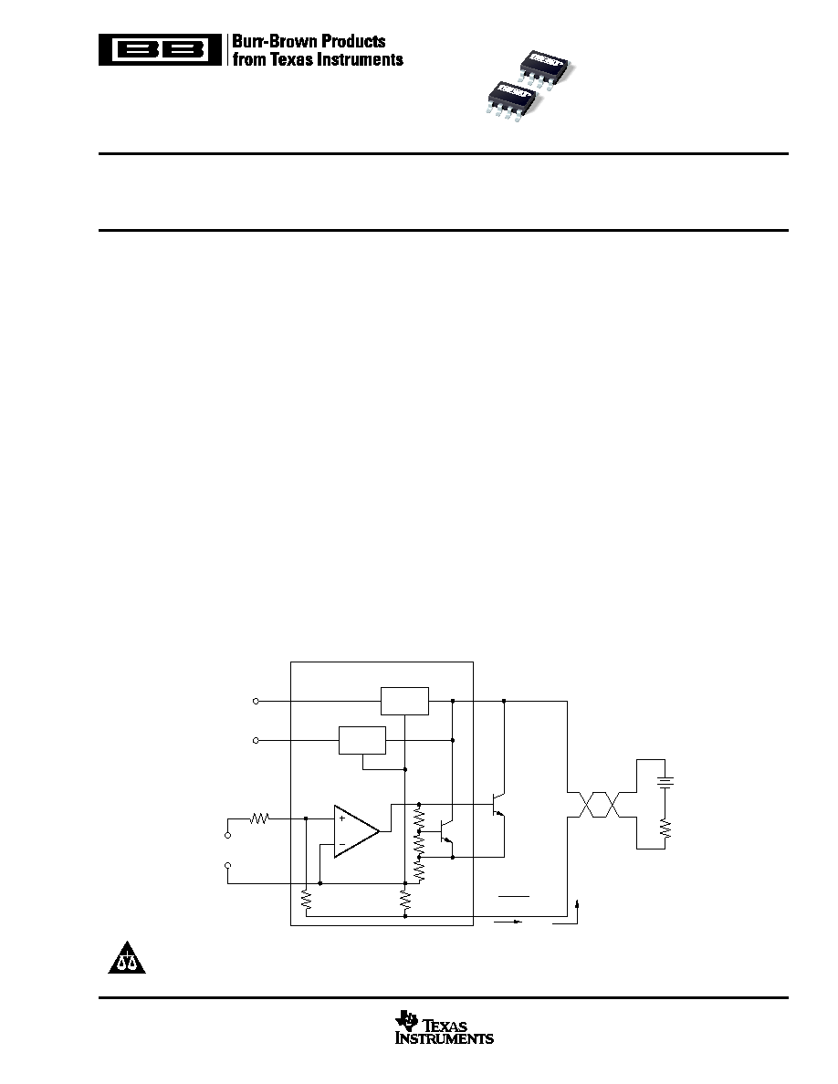
The XTR115 and XTR116 are precision current out-
put converters designed to transmit analog 4-to-20mA
signals over an industry standard current loop. They
provide accurate current scaling and output current
limit functions.
The on-chip voltage regulator (5V) can be used to
power external circuitry. A precision on-chip V
REF
(2.5V for XTR115 and 4.096V for XTR116) can be
used for offsetting or to excite transducers. A current
return pin (I
RET
) senses any current used in external
circuitry to assure an accurate control of the output
current.
The XTR115 is a fundamental building block of
smart sensors using 4-to-20mA current transmission.
The XTR115 and XTR116 are specified for opera-
tion over the extended industrial temperature range,
40
°
C to +85
°
C.
XTR115
XTR116
R
IN
I
IN
V
IN
+
I
RET
XTR115
XTR116
+5V
Regulator
R
2
25
R
LIM
E
B
V+
R
1
2.475k
I
O
=
100 V
IN
R
IN
A1
Voltage
Reference
+5V
V
REG
V
REF
2
3
8
1
5
4
7
6
XTR115: 2.5V
XTR116: 4.096V
R
L
V
LOOP
I = 100
· I
IN
SBOS124A JANUARY 2000 REVISED NOVEMBER 2003
www.ti.com
PRODUCTION DATA information is current as of publication date.
Products conform to specifications per the terms of Texas Instruments
standard warranty. Production processing does not necessarily include
testing of all parameters.
Copyright © 2000-2003, Texas Instruments Incorporated
Please be aware that an important notice concerning availability, standard warranty, and use in critical applications of
Texas Instruments semiconductor products and disclaimers thereto appears at the end of this data sheet.
All trademarks are the property of their respective owners.

XTR115, XTR116
2
SBOS124A
www.ti.com
Specifications the same as XTR115U and XTR116U.
NOTES: (1) Does not include initial error or TCR of R
IN
. (2) Voltage measured with respect to I
RET
pin.
SPECIFICATIONS
At T
A
= +25
°
C, V+
= 24V, R
IN
= 20k
, and TIP29C external transistor, unless otherwise noted.
XTR115U
XTR115UA
XTR116U
XTR116UA
PARAMETER
CONDITIONS
MIN
TYP
MAX
MIN
TYP
MAX
UNITS
OUTPUT
Output Current Equation
I
O
I
O
= I
IN
· 100
Output Current, Linear Range
0.25
25
mA
Over-Scale Limit
I
LIM
32
mA
Under-Scale Limit
I
MIN
I
REG
= 0, I
REF
= 0
0.2
0.25
mA
SPAN
Span (Current Gain)
S
100
A/A
Error
(1)
I
IN
= 250
µ
A to 25mA
±
0.05
±
0.2
±
0.4
%
vs Temperature
T
A
= 40
°
C to +85
°
C
±
3
±
20
ppm/
°
C
Nonlinearity
I
IN
= 250
µ
A to 25mA
±
0.003
±
0.01
±
0.02
%
INPUT
Offset Voltage (Op Amp)
V
OS
I
IN
= 40
µ
A
±
100
±
250
±
500
µ
V
vs Temperature
T
A
= 40
°
C to +85
°
C
±
0.7
±
3
±
6
µ
V/
°
C
vs Supply Voltage, V+
V+ = 7.5V to 36V
±
0.1
±
2
µ
V/V
Bias Current
I
B
35
nA
vs Temperature
150
pA/
°
C
Noise: 0.1Hz to 10Hz
e
n
0.6
µ
Vp-p
DYNAMIC RESPONSE
Small Signal Bandwidth
C
LOOP
= 0, R
L
= 0
380
kHz
Slew Rate
3.2
mA/
µ
s
V
REF
(2)
XTR115
2.5
V
XTR116
4.096
V
Voltage Accuracy
I
REF
= 0
±
0.05
±
0.25
±
0.5
%
vs Temperature
T
A
= 40
°
C to +85
°
C
±
20
±
35
±
75
ppm/
°
C
vs Supply Voltage, V+
V+ = 7.5V to 36V
±
1
±
10
ppm/V
vs Load
I
REF
= 0mA to 2.5mA
±
100
ppm/mA
Noise: 0.1Hz to 10Hz
10
µ
Vp-p
Short-Circuit Current
16
mA
V
REG
(2)
Voltage
5
V
Voltage Accuracy
I
REG
= 0
±
0.05
±
0.1
V
vs Temperature
T
A
= 40
°
C to +85
°
C
±
0.1
mV/
°
C
vs Supply Voltage, V+
V+ = 7.5V to 36V
1
mV/V
vs Output Current
See Typical Curves
Short-Circuit Current
12
mA
POWER SUPPLY
V+
Specified
+24
V
Voltage Range
+7.5
+36
V
Quiescent Current
200
250
µ
A
Over Temperature, 40
°
C to +85
°
C
240
300
µ
A
TEMPERATURE RANGE
Specification
40
+85
°
C
Operating
55
+125
°
C
Storage
55
+125
°
C
Thermal Resistance
JA
150
°
C/W
XTR115, XTR116
3
SBOS124A
www.ti.com
Power Supply, V+ (referenced to I
O
pin) .......................................... 40V
Input Voltage (referenced to I
RET
pin) ........................................ 0V to V+
Output Current Limit ............................................................... Continuous
V
REG
, Short-Circuit .................................................................. Continuous
V
REF
, Short-Circuit .................................................................. Continuous
Operating Temperature ................................................ 55
°
C to +125
°
C
Storage Temperature Range ....................................... 55
°
C to +125
°
C
Lead Temperature (soldering, 10s) .............................................. +300
°
C
Junction Temperature ................................................................... +165
°
C
NOTE: (1) Stresses above these ratings may cause permanent damage.
Exposure to absolute maximum conditions for extended periods may degrade
device reliability.
ABSOLUTE MAXIMUM RATINGS
(1)
Top View
SO-8
PIN CONFIGURATION
PACKAGE/ORDERING INFORMATION
V
REF
I
IN
I
RET
I
O
V
REG
V+
B (Base)
E (Emitter)
1
2
3
4
8
7
6
5
ELECTROSTATIC
DISCHARGE SENSITIVITY
This integrated circuit can be damaged by ESD. Texas Instru-
ments recommends that all integrated circuits be handled with
appropriate precautions. Failure to observe proper handling
and installation procedures can cause damage.
ESD damage can range from subtle performance degrada-
tion to complete device failure. Precision integrated circuits
may be more susceptible to damage because very small
parametric changes could cause the device not to meet its
published specifications.
For the most current package and ordering information, see
the Package Option Addendum located at the end of this
data sheet.
XTR115, XTR116
4
SBOS124A
www.ti.com
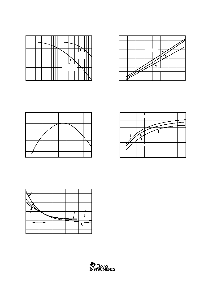
TYPICAL PERFORMANCE CURVES
At T
A
= +25
°
C, V+
= 24V, R
IN
= 20k
, and TIP29C external transistor, unless otherwise noted.
10k
100k
Frequency (Hz)
CURRENT GAIN vs FREQUENCY
1M
40
30
20
10
Gain (dB)
C
OUT
= 10nF
R
L
= 250
C
OUT
= 0
R
L
= 0
75
50
25
0
25
50
75
100
Temperature (
°
C)
REFERENCE VOLTAGE vs TEMPERATURE
125
0.1
0
0.1
0.2
0.3
Reference Voltage (%)
75
50
25
0
25
50
75
100
Temperature (
°
C)
QUIESCENT CURRENT vs TEMPERATURE
125
260
240
220
200
180
160
Quiescent Current (
µ
A)
(V+) = 36V
(V+) = 24V
(V+) = 7.5V
75
50
25
0
25
50
75
100
Temperature (
°
C)
OVER-SCALE CURRENT vs TEMPERATURE
125
34
33
32
31
30
29
28
Over-Scale Current (mA)
V+ = 7.5V
V+ = 36V
V+ = 24V
With External Transistor
1
0
1
2
3
I
REG
Current (mA)
V
REG
VOLTAGE vs V
REG
CURRENT
4
5.5
5.0
4.5
V
REG
Voltage (V)
+25
°
C
+25
°
C
55
°
C
+125
°
C
Sinking
Current
Sourcing
Current
55
°
C
+125
°
C
XTR115, XTR116
5
SBOS124A
www.ti.com
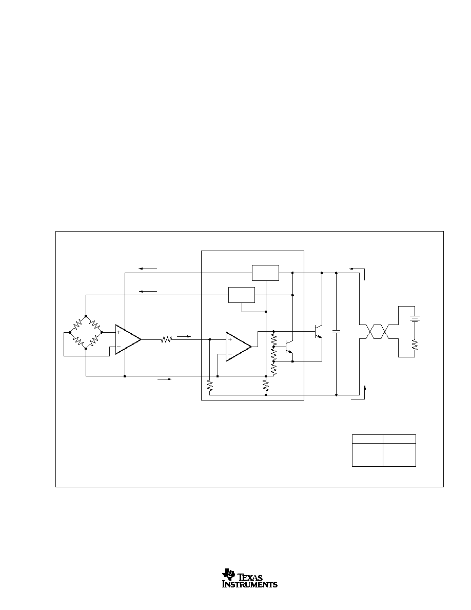
APPLICATIONS INFORMATION
The XTR115 and XTR116 are identical devices except for
the reference voltage output, pin 1. This voltage is available
for external circuitry and is not used internally. Further
discussions that apply to both devices will refer to the
"XTR115/6."
Figure 1 shows basic circuit connections with representative
simplified input circuitry. The XTR115/6 is a two-wire
current transmitter. Its input signal (pin 2) controls the output
current. A portion of this current flows into the V+ power
supply, pin 7. The remaining current flows in Q1. External
input circuitry connected to the XTR115/6 can be powered
from V
REG
or V
REF
. Current drawn from these terminals
must be returned to I
RET
, pin 3. This I
RET
pin is a "local
ground" for input circuitry driving the XTR115/6.
The XTR115/6 is a current-input device with a gain of 100.
A current flowing into pin 2 produces I
O
= 100 · I
IN
. The
input voltage at the I
IN
pin is zero (referred to the I
RET
pin).
A voltage input is created with an external input resistor, as
shown. Common full-scale input voltages range from 1V
and upward. Full-scale inputs greater than 0.5V are recom-
mend to minimize the effect of offset voltage and drift of A1.
EXTERNAL TRANSISTOR
The external transistor, Q1, conducts the majority of the full-
scale output current. Power dissipation in this transistor can
approach 0.8W with high loop voltage (40V) and 20mA
output current. The XTR115/6 is designed to use an external
transistor to avoid on-chip thermal-induced errors. Heat
produced by Q1 will still cause ambient temperature changes
that can affect the XTR115/6. To minimize these effects,
locate Q1 away from sensitive analog circuitry, including
XTR115/6. Mount Q1 so that heat is conducted to the
outside of the transducer housing.
The XTR115/6 is designed to use virtually any NPN transis-
tor with sufficient voltage, current and power rating. Case
style and thermal mounting considerations often influence
the choice for any given application. Several possible choices
are listed in Figure 1. A MOSFET transistor will not improve
the accuracy of the XTR115/6 and is not recommended.
R
IN
20k
I
IN
2
V
IN
I
RET
3
XTR115
XTR116
+5V
Regulator
R
2
25
R
LIM
E
5
I
O
4
B
6
V+
7
R
1
2.475k
R
L
V
LOOP
A1
Voltage
Reference
V
REG
5V
V
REF
(1)
8
1
XTR115: 2.5V
XTR116: 4.096V
Possible choices for Q
1
(see text).
2N4922
TIP29C
TIP31B
TYPE
TO-225
TO-220
TO-220
PACKAGE
I = 100
· I
IN
I
O
10nF
I
REF
I
IN
All return current
from I
REG
and I
REF
For I
O
= 4mA to 20mA
I
IN
= 40
µ
A to 200
µ
A
With R
IN
= 20k
V
IN
= 0.8V to 4V
I
REG
Q
1
Input
Circuitry
NOTE: (1) See also Figure 5.
FIGURE 1. Basic Circuit Connections.
XTR115, XTR116
6
SBOS124A
www.ti.com
MINIMUM-SCALE CURRENT
The quiescent current of the XTR115/6 (typically 200
µ
A)
is the lower limit of its output current. Zero input current
(I
IN
= 0) will produce an I
O
equal to the quiescent current.
Output current will not begin to increase until I
IN
> I
Q
/100.
Current drawn from V
REF
or V
REG
will add to this minimum
output current. This means that more than 3.7mA is avail-
able to power external circuitry while still allowing the
output current to go below 4mA.
OFFSETTING THE INPUT
A low scale of 4mA is produced by creating a 40
µ
A input
current. This can be created with the proper value resistor
from V
REF
(Figure 2), or by generating offset in the input
drive circuitry.
I
IN
I
RET
XTR115
R
1
2.475k
R
0
62.5k
A1
Voltage
Reference
V
REG
V
REF
2.5V
40
µ
A
0 to 160
µ
A
MAXIMUM OUTPUT CURRENT
The XTR115/6 provides accurate, linear output up to 25mA.
Internal circuitry limits the output current to approximately
32mA to protect the transmitter and loop power/measure-
ment circuitry.
It is possible to extend the output current range of the
XTR115/6 by connecting an external resistor from pin 3 to
pin 5, to change the current limit value. Since all output
current must flow through internal resistors, it is possible to
damage with excessive current. Output currents greater than
45mA may cause permanent damage.
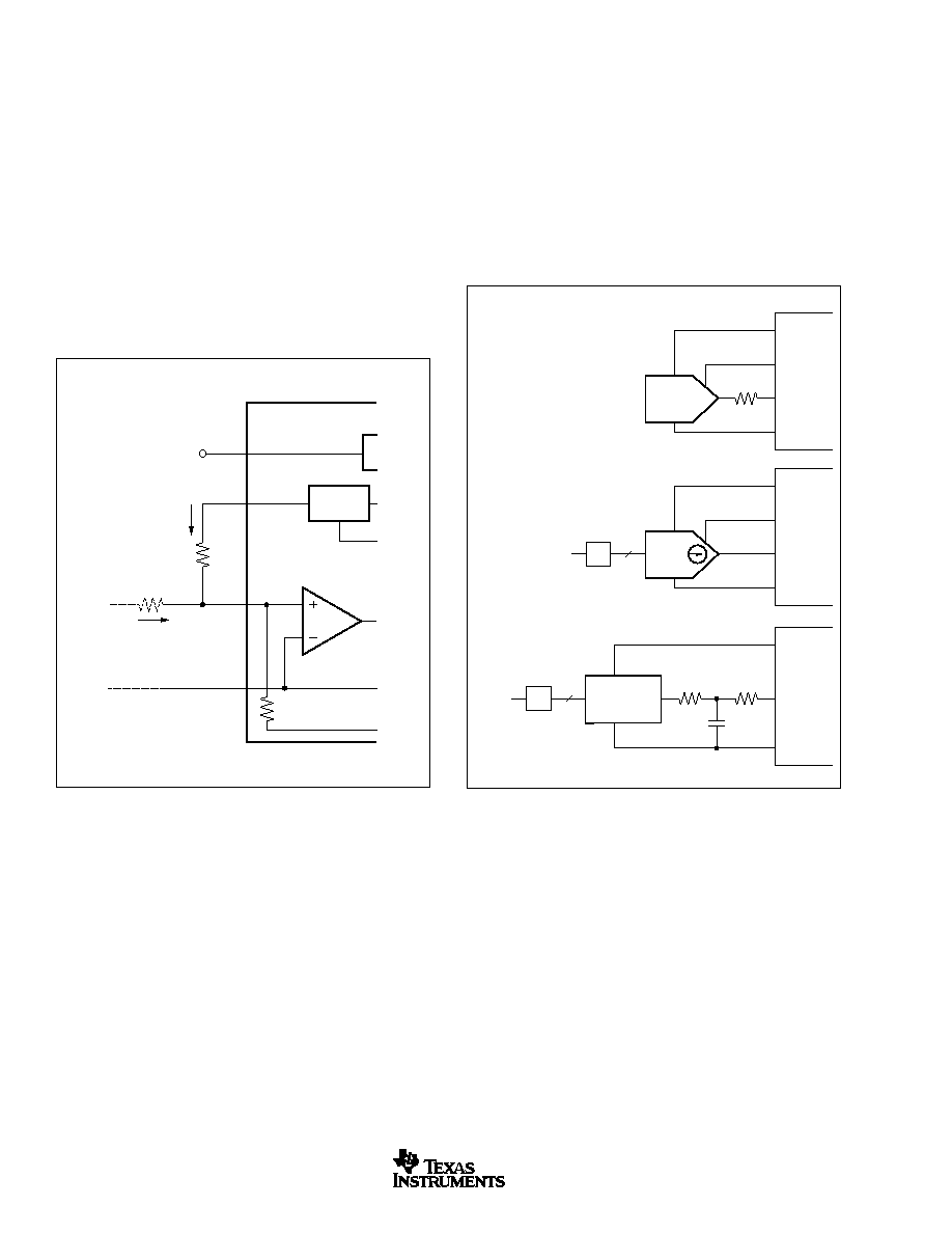
XTR115
XTR116
V
O
D/A
R
IN
V
REF
V
REG
XTR115
XTR116
I
O
D/A
Optical
Isolation
Optical
Isolation
Digital
Control
I
IN
I
RET
V
REF
V
REG
XTR115
XTR116
µ
C
PWM
Out
Digital
Control
R
IN
Filter
I
RET
V
REG
5V
FIGURE 2. Creating Low-Scale Offset.
FIGURE 3. Digital Control Methods.
XTR115, XTR116
7
SBOS124A
www.ti.com
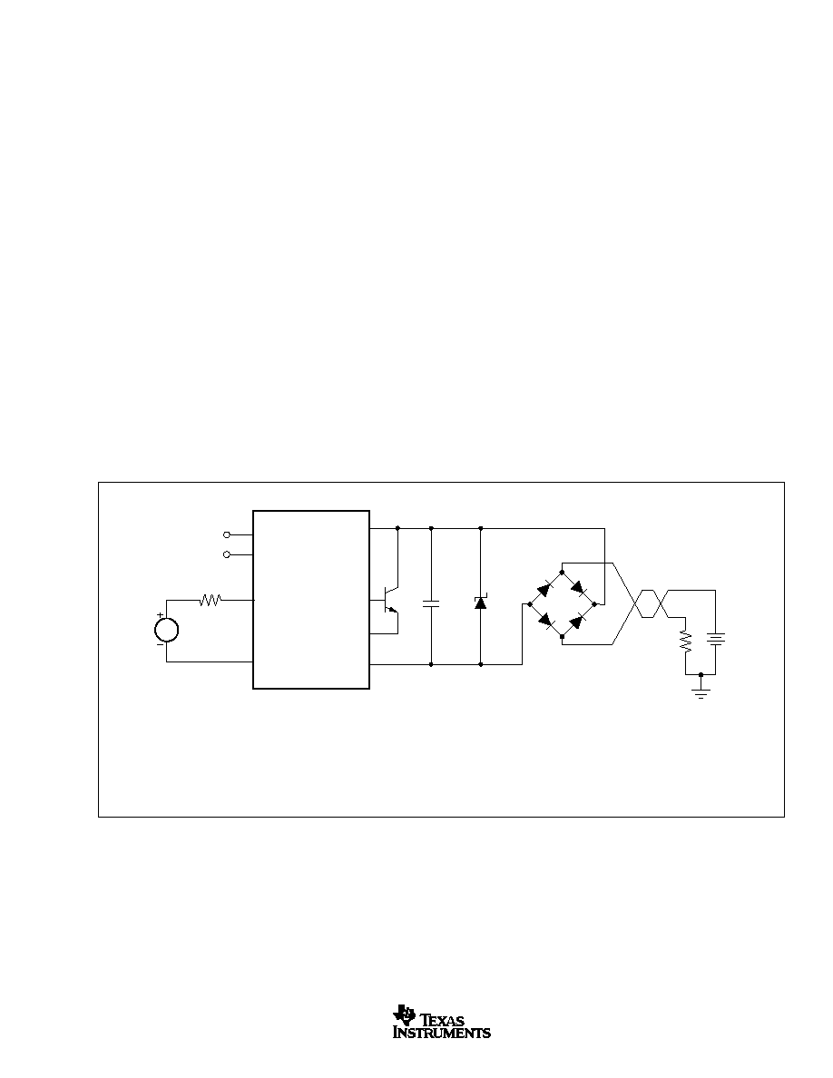
V
PS
0.01
µ
F
R
L
D
1
(1)
NOTE: (1) Zener Diode 36V: 1N4753A or Motorola
P6KE39A. Use lower voltage zener diodes with loop
power supply voltages less than 30V for increased
protection. See "Over-Voltage Surge Protection."
Maximum V
PS
must be
less than minimum
voltage rating of zener
diode.
The diode bridge causes
a 1.4V loss in loop supply
voltage.
1N4148
Diodes
8
1
2
3
XTR115
XTR116
V
IN
V
REF
I
IN
I
RET
V
REG
V+
I
O
E
B
6
7
5
4
Q
1
R
IN
FIGURE 4. Reverse Voltage Operation and Over-Voltage Surge Protection.
REVERSE-VOLTAGE PROTECTION
The XTR115/6 low compliance voltage rating (7.5V) per-
mits the use of various voltage protection methods without
compromising operating range. Figure 4 shows a diode
bridge circuit which allows normal operation even when the
voltage connection lines are reversed. The bridge causes a
two diode drop (approximately 1.4V) loss in loop supply
voltage. This results in a compliance voltage of approxi-
mately 9V--satisfactory for most applications. A diode can
be inserted in series with the loop supply voltage and the V+
pin to protect against reverse output connection lines with
only a 0.7V loss in loop supply voltage.
OVER-VOLTAGE SURGE PROTECTION
Remote connections to current transmitters can sometimes be
subjected to voltage surges. It is prudent to limit the maximum
surge voltage applied to the XTR115/6 to as low as practical.
Various zener diode and surge clamping diodes are specially
designed for this purpose. Select a clamp diode with as low a
voltage rating as possible for best protection. For example, a
36V protection diode will assure proper transmitter operation
at normal loop voltages, yet will provide an appropriate level
of protection against voltage surges. Characterization tests on
several production lots showed no damage with loop supply
voltages up to 65V.
Most surge protection zener diodes have a diode character-
istic in the forward direction that will conduct excessive
current, possibly damaging receiving-side circuitry if the
loop connections are reversed. If a surge protection diode is
used, a series diode or diode bridge should be used for
protection against reversed connections.
RADIO FREQUENCY INTERFERENCE
The long wire lengths of current loops invite radio frequency
interference. RF can be rectified by the input circuitry of the
XTR115/6 or preceding circuitry. This generally appears as
an unstable output current that varies with the position of
loop supply or input wiring.
Interference may also enter at the input terminals. For
integrated transmitter assemblies with short connection to
the sensor, the interference more likely comes from the
current loop connections.
XTR115, XTR116
8
SBOS124A
www.ti.com
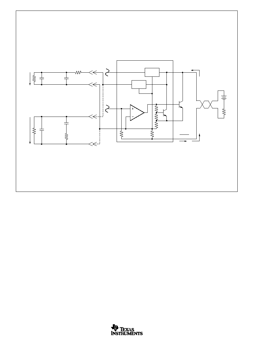
FIGURE 5. Stable Operation with Capacitive Load on V
REF
.
I
IN
2
I
RET
3
XTR115
XTR116
+5V
Regulator
R
2
25
R
LIM
E
5
4
B
6
V+
7
R
1
2.475k
R
L
V
LOOP
A1
Voltage
Reference
V
REG
V
REF
8
1
I = 100
· I
IN
I
O
If capacitive loading must be placed on the V
REF
pin, one of the compensation schemes shown below must be used to ensure stable operation.
Values of capacitance must remain within the given ranges.
NOTE: (1) Required compensation components.
I
O
=
100 V
IN
R
IN
+
R
ISO
(1)
10
C
LF
(2.2
µ
F to 22
µ
F)
C
HF
(10pF to 0.5
µ
F)
+
C
LF
(1)
(2.2
µ
F to 22
µ
F)
R
COMP
(1)
50
C
HF
(10pF to 0.5
µ
F)
OR
I
LOAD
(0-2.5mA)
I
LOAD
(0-2.5mA)
PACKAGING INFORMATION
ORDERABLE DEVICE
STATUS(1)
PACKAGE TYPE
PACKAGE DRAWING
PINS
PACKAGE QTY
XTR115U
ACTIVE
SOIC
D
8
100
XTR115U/2K5
ACTIVE
SOIC
D
8
2500
XTR115UA
ACTIVE
SOIC
D
8
100
XTR115UA/2K5
ACTIVE
SOIC
D
8
2500
XTR116U
ACTIVE
SOIC
D
8
100
XTR116U/2K5
ACTIVE
SOIC
D
8
2500
XTR116UA
ACTIVE
SOIC
D
8
100
XTR116UA/2K5
ACTIVE
SOIC
D
8
2500
(1) The marketing status values are defined as follows:
ACTIVE: Product device recommended for new designs.
LIFEBUY: TI has announced that the device will be discontinued, and a lifetime-buy period is in effect.
NRND: Not recommended for new designs. Device is in production to support existing customers, but TI does not recommend using this part in
a new design.
PREVIEW: Device has been announced but is not in production. Samples may or may not be available.
OBSOLETE: TI has discontinued the production of the device.
PACKAGE OPTION ADDENDUM
www.ti.com
21-Oct-2003
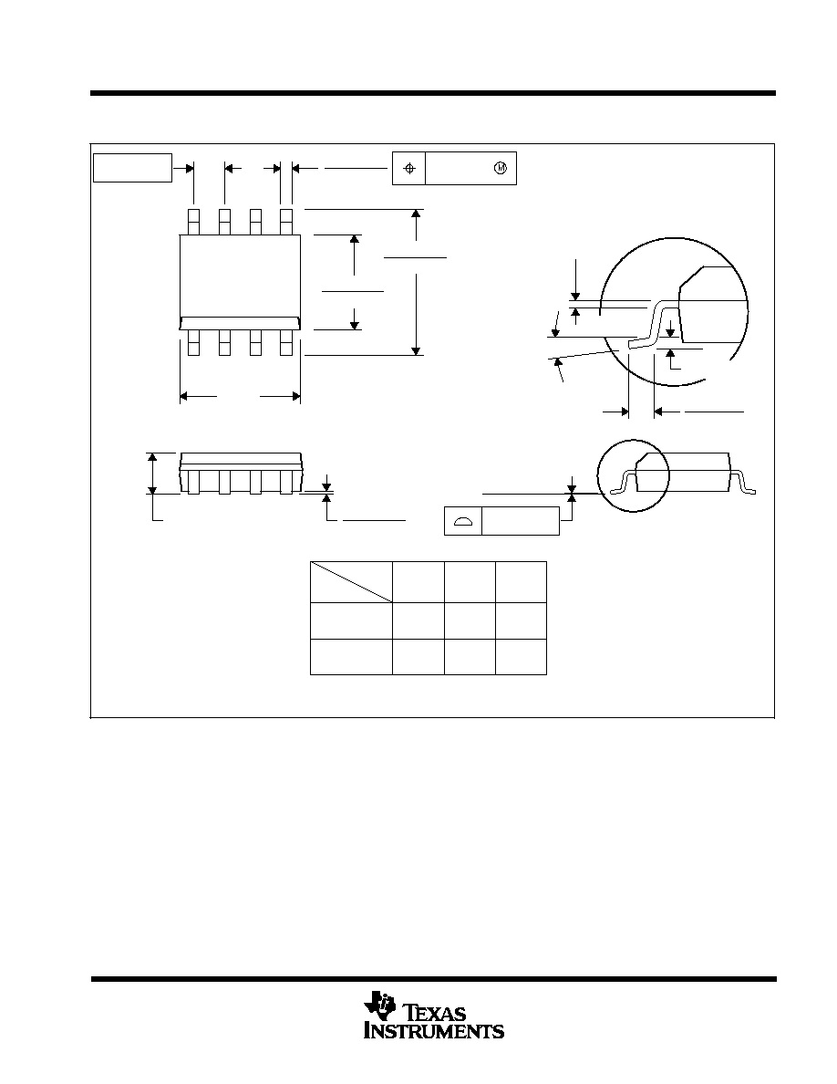
MECHANICAL DATA
MSOI002B JANUARY 1995 REVISED SEPTEMBER 2001
POST OFFICE BOX 655303
·
DALLAS, TEXAS 75265
D (R-PDSO-G**)
PLASTIC SMALL-OUTLINE PACKAGE
8 PINS SHOWN
8
0.197
(5,00)
A MAX
A MIN
(4,80)
0.189
0.337
(8,55)
(8,75)
0.344
14
0.386
(9,80)
(10,00)
0.394
16
DIM
PINS **
4040047/E 09/01
0.069 (1,75) MAX
Seating Plane
0.004 (0,10)
0.010 (0,25)
0.010 (0,25)
0.016 (0,40)
0.044 (1,12)
0.244 (6,20)
0.228 (5,80)
0.020 (0,51)
0.014 (0,35)
1
4
8
5
0.150 (3,81)
0.157 (4,00)
0.008 (0,20) NOM
0
°
8
°
Gage Plane
A
0.004 (0,10)
0.010 (0,25)
0.050 (1,27)
NOTES: A. All linear dimensions are in inches (millimeters).
B. This drawing is subject to change without notice.
C. Body dimensions do not include mold flash or protrusion, not to exceed 0.006 (0,15).
D. Falls within JEDEC MS-012

IMPORTANT NOTICE
Texas Instruments Incorporated and its subsidiaries (TI) reserve the right to make corrections, modifications,
enhancements, improvements, and other changes to its products and services at any time and to discontinue
any product or service without notice. Customers should obtain the latest relevant information before placing
orders and should verify that such information is current and complete. All products are sold subject to TI's terms
and conditions of sale supplied at the time of order acknowledgment.
TI warrants performance of its hardware products to the specifications applicable at the time of sale in
accordance with TI's standard warranty. Testing and other quality control techniques are used to the extent TI
deems necessary to support this warranty. Except where mandated by government requirements, testing of all
parameters of each product is not necessarily performed.
TI assumes no liability for applications assistance or customer product design. Customers are responsible for
their products and applications using TI components. To minimize the risks associated with customer products
and applications, customers should provide adequate design and operating safeguards.
TI does not warrant or represent that any license, either express or implied, is granted under any TI patent right,
copyright, mask work right, or other TI intellectual property right relating to any combination, machine, or process
in which TI products or services are used. Information published by TI regarding third-party products or services
does not constitute a license from TI to use such products or services or a warranty or endorsement thereof.
Use of such information may require a license from a third party under the patents or other intellectual property
of the third party, or a license from TI under the patents or other intellectual property of TI.
Reproduction of information in TI data books or data sheets is permissible only if reproduction is without
alteration and is accompanied by all associated warranties, conditions, limitations, and notices. Reproduction
of this information with alteration is an unfair and deceptive business practice. TI is not responsible or liable for
such altered documentation.
Resale of TI products or services with statements different from or beyond the parameters stated by TI for that
product or service voids all express and any implied warranties for the associated TI product or service and
is an unfair and deceptive business practice. TI is not responsible or liable for any such statements.
Following are URLs where you can obtain information on other Texas Instruments products and application
solutions:
Products
Applications
Amplifiers
amplifier.ti.com
Audio
www.ti.com/audio
Data Converters
dataconverter.ti.com
Automotive
www.ti.com/automotive
DSP
dsp.ti.com
Broadband
www.ti.com/broadband
Interface
interface.ti.com
Digital Control
www.ti.com/digitalcontrol
Logic
logic.ti.com
Military
www.ti.com/military
Power Mgmt
power.ti.com
Optical Networking
www.ti.com/opticalnetwork
Microcontrollers
microcontroller.ti.com
Security
www.ti.com/security
Telephony
www.ti.com/telephony
Video & Imaging
www.ti.com/video
Wireless
www.ti.com/wireless
Mailing Address:
Texas Instruments
Post Office Box 655303 Dallas, Texas 75265
Copyright
2003, Texas Instruments Incorporated