 | –≠–ª–µ–∫—Ç—Ä–æ–Ω–Ω—ã–π –∫–æ–º–ø–æ–Ω–µ–Ω—Ç: T231-DIE | –°–∫–∞—á–∞—Ç—å:  PDF PDF  ZIP ZIP |
GENERAL DESCRIPTION
TLSI's family of VCXO Clock Generators is ideally
suited for a wide range of applications in which cost,
size, power, and the number of discrete components
need to be minimized. These ICs are designed to
exhibit excellent temperature stability and phase
noise performance. The T231 features fundamental
crystal operation over a frequency range that
includes SONET and other communication protocols.
Typical tuning frequency range is ± 50 PPM (crystal
and varactor dependent). Differential PECL outputs
are provided in the T231 to help reduce the effects
of noise and distortion.
FEATURES
∑
Fundamental Crystal Frequency
∑
Supply Voltage 3.0V to 5.5V
∑
Operating Temperature -40∞C to +85∞C
∑
Power Less than 150 mW
∑
Start-Up Time Less than 5 mS
∑
Phase Noise at 100 kHz Offset from Fc less
than ≠135 dBc/Hz
∑
Rise and Fall Times Less than 1 nS
∑
Nominal Output Duty Cycle 45% to 55%
∑
Output Drive Capability of 5 pF at 200 MHz
∑
Tuning Input Impedance 50 k
∑
Internal Crystal Load Capacitance 15pF
T 23 1
V C X O C l o c k G e n e r a t o r I C
1 0 0 M H z t o 2 0 0 M H z
P
R
E
L
I
M
I
N
A
R
Y
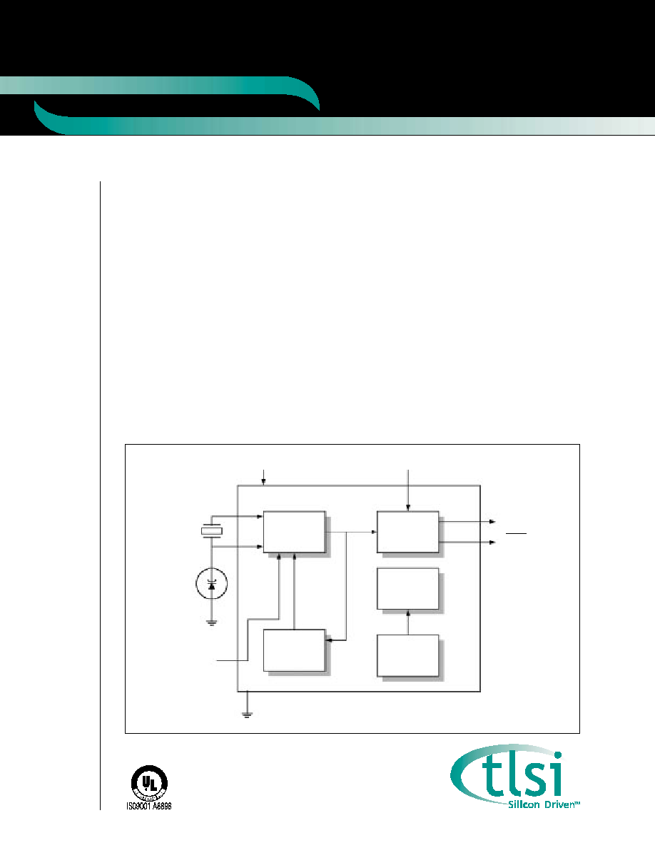
BLOCK DIAGRAM
VDD
VSS
T231 VCXO Clock Generator IC Block Diagram
VCTRL
FOUT
XTAL
XTL1
XTL2
OE
FOUT
OUTPUT DRIVER
VARAC TOR
OSCILLATOR
POWER ON
RESET
AMPLITUDE
CONTROL
REFERENCE
SUPPLY
PARAMETER CONDITIONS
UNITS
Supply Voltage
V
SS
- 0.5
V
DD
5.5 V
DC Input Voltage
V
SS
- 0.5
V
IN
V
DD
+ 0.5
V
DC Output Voltage
V
SS
- 0.5
V
OUT
V
DD
+ 0.5
V
Storage Temperature
-65 < T
S
< +150
∞C
Ambient Temperature -40 < T
A
< +85
∞C
Junction Temperature
-65 < T
J
< +125
∞C
Soldering Temperature
T
SLDR
< 260 for less than 10 seconds
∞C
ABSOLUTE MAXIMUM RATINGS*
* Operation of the device at or beyond these specifications may result in permanent damage or
affect operation and reliability of the product.
PARAMETER CONDITIONS
SYMBOL
MIN
TYP
MAX
UNITS
Supply Voltage
V
DD
3.0 5.0 5.5 V
High-Level Output Voltage
V
OH
V
DD
-
V
1.02
Low-Level Output Voltage
V
OL
V
DD
-
V
1.62
High-Level Input Voltage
V
I H
4.0
Low-Level Input Voltage
V
I L
1.0 V
OE High-Level Input Current
I
I H
1.0
µA
OE Low-Level Input Current
I
I L
-50
µA
Supply Current
F=200 MHz,C
L
=5 pF
I
DD
18.0 25.0 mA
Tuning Range
(See Tuning Range Section)
f
±
50
ppm
Crystal Drive
V
XTL
1.0 Vpp
Short-Circuit Source Current
< 20 seconds
I
OSH
-24 mA
Short-Circuit Sink Current
< 20 seconds`
I
OS L
24 mA
ELECTRICAL CHARACTERISTICS
DC CHARACTERISTICS
V
DD
= 5.0 V, -40 ∞C < T
A
< +85 ∞C unless otherwise specified
2
3
ELECTRICAL CHARACTERISTICS (continued)
AC CHARACTERISTICS
V
DD
= 5.0 V, -40 ∞C < T
A
< +85 ∞C unless otherwise specified
TUNING RANGE
Tuning Range depends on the design of the crystal, the capacitance loading of the printed circuit
board and the variable capacitance of the varactor loading the T231 IC. The parallel resonant
frequency of the crystal with any external capacitive loading is greater than the fixed series resonant
frequency of the crystal by
f:
f = Cx10
6
/2(C
O
+C
P
) ppm
where C is the series mechanical capacitance of the crystal, C
O
is the parallel capacitance of the
crystal, and C
P
is the additional loading capacitance used to tune the crystal. The loading capacitance
is the equivalent capacitance of the 15 pF internal load capacitance in series with the varactor
capacitance. All capacitance are in units of picofarads.
Example:
For a typical crystal, C = 0.05 pF and C
O
= 4 pF. Using a Hyperabrupt Tuning Diode, the
typical capacitance of the diode is 12.3 pF at 1 volt and 2.60 pf at 3 volts. The varactor diode
appears in series with the 15 pF internal chip capacitance. In addition, assuming 2 pF stray board
wiring capacitance across both the varactor and the chip terminals, the following calculations
determine the pullability of the oscillator:
Frequency shift with 1 volt across the varactor diode:
C
P
= 15 pF + 2 pF in series with 12.3 pF + 2 pF = (17.0x14.3)/(17.0+14.3) pF = 7.77 pF
f
1
= 0.005x10
6
/(2(4.00+7.77) ppm = 212.4 ppm
Frequency shift with 3 volts across the varactor diode:
C
P
= 15 pF + 2 pF in series with 2.60 pF + 2 pF = (17.0x4.60)/(17.0+4.60) pF = 3.62 pF
f
2
= 0.005x10
6
/(2(4.00+3.62) ppm = 328.1 ppm
Total Tuning Range = 328.1 ppm - 212.4 ppm = 116 ppm
PARAMETER CONDITIONS
SYMBOL
MIN
TYP
MAX
UNITS
Crystal Frequency Range
F
XTL
100 200
MHz
Output Duty Cycle
ODC
45 55
%
Power-Up Interval
T
ON
2.5
5.0
mS
Output Jitter
RMS, 12kHz to 20 MHz
J
O
1
pS
Rise and Fall Time
C
L
=5 pF
t
r
,t
f
2
nS
Rise and Fall Time,
C
L
=5 pF
t
r
,t
f
1
nS
High Speed Version
Phase Noise
100 kHz offset from F
c
N
PH
-135 dBc/Hz
Temperature Stability
F
TEMP
±
15 ppm
Frequency vs. Load Capacitance
F
LC
1
ppm
Frequency vs. Supply Voltage
F
SV
2
ppm
Tuning Input Impedance
Z
TUNE
50 100
k
L
C
P
C
Oscillator Equivalent Circuit
R
C0
4
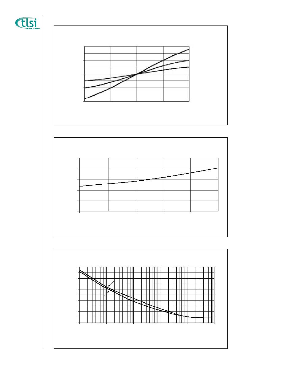
GRAPHS OF TYPICAL OPERATING CONDITIONS
4.5
100 120 140
160 180
10
fo = 100 MHz
fo = 200 MHz
-50
-60
-70
-80
-90
-100
-110
-120
-130
-140
-150
100
1000
10000
100000
1000000
20
18
16
14
12
10
1
0.5
0
-0.5
-1
4.75
VDD, volts
Frequency, MHz
Frequency Offset from fo, Hz
Fr
equency Shift, ppm
Supply Curr
ent, mA
Phase Noise, dBc/Hz
5
5.25
5.5
VTCRL = 5.0 V
VTCRL = 2.5 V
VTCRL = 0.5 V
Frequency Shift vs. VDD, T = 25∞C
Supply Current vs. Frequency
Phase Noise vs. Frequency Offset
5
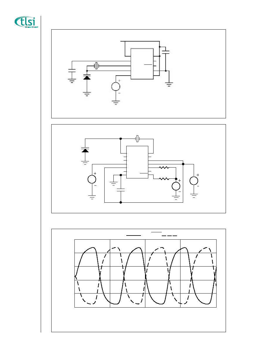
TEST CIRCUIT SCHEMATIC
OUTPUT WAVEFORMS
4.2
4.0
3.8
3.6
3.4
3.2
VCTRL
VARACTOR
CBYPASS
VDD
0.01 µF
1
2
3
4
5
10
9
8
7
6
VDD
AGC
XTL1
XTL2
VCTRL
VDD
FOUT
FOUT
VSS
OE
T231
V
olts
Nanoseconds
FOUT 155.52MHz
T231 TEST CIRCUIT 10-Pin MSOP Configuration
V
0.0
5.0
10
15 20
FOUT
FOUT
VSUPPLY
5V
VCTRL
XTAL
CBYPASS
50
50
3V
1
2
3
4
5
6
7
14
13
12
11
10
9
8
XTL2
NC
NC
VCTRL
OE
NC
VSS
XTL1
NC
VDD
VDD
FOUT
NC
FOUT
T231
T231 TEST CIRCUIT 14-Pin SOIC Configuration
V
V
V
VARACTOR