TE
CH
tm
Preliminary T2316407A
Taiwan Memory Technology, Inc. reserves the right
P. 1
Publication Date: APR 2001
to change products or specifications without notice.
Revision:0.B
T2316405A
DRAM
4M x 4 DYNAMIC RAM
EDO PAGE MODE
FEATURES
∑
Industry-standard x 4 pinouts and timing
functions
∑
power supply : T2316405A 2.6V(±0.2V)
T2316407A 3.3V(±0.3V)
∑
All device pins are TTL- compatible.
∑
2048-cycle refresh in 32 ms.
∑
Refresh modes: RAS only, CAS BEFORE
RAS (CBR) and HIDDEN.
∑
Extended data-out (EDO) PAGE MODE
access cycle.
OPTION
TIMING
MARKING
50ns (For T2316407A only) -50
60ns (For T2316407A only) -60
70ns (For T2316407A only) -70
100ns (For T2316405A only) -10
PACKAGE
26/24-pin SOJ
J
26/24-pin TSOP-II S
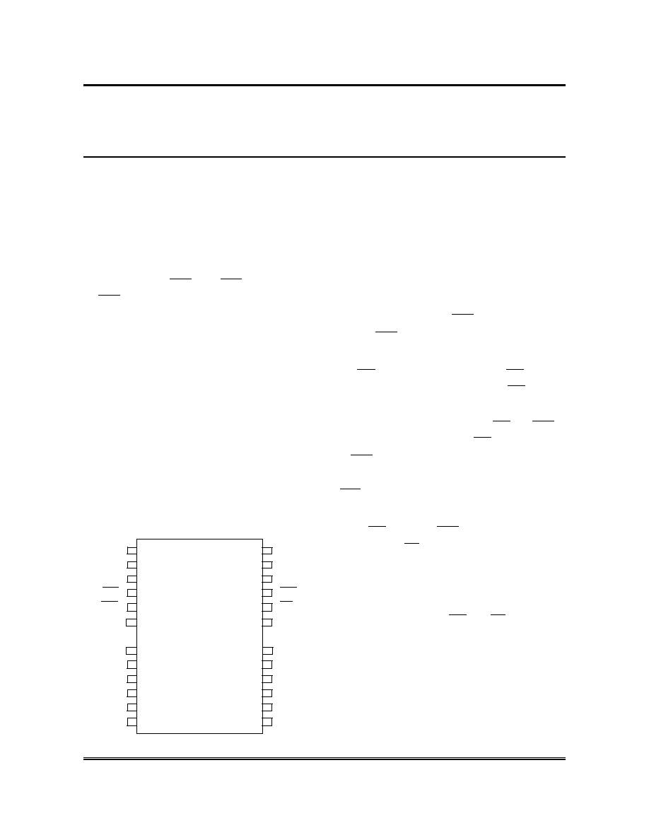
PIN ARRANGEMENT (Top View)
I/O1
Vcc
NC
A10
A0
A1
A2
26
25
24
23
22
18
17
16
15
14
1
2
3
4
5
9
10
11
12
13
I/O4
Vss
I/O3
A8
A7
A6
A5
A4
OE
CAS
6
WE
RAS
I/O2
19
8
Vss
21
Vcc
A3
A9
SOJ
&
TSOP-II
GRNERAL DESCRIPTION
The T2316405A and T2316407A is a randomly
accessed solid state memory containing 16,777,216
bits organized in a x 4 configuration. It offers Fast
Page mode with Extended Data Output (EDO).
During READ or WRITE cycles, each of the 4
memory bits (1 bit per I/O) is uniquely addressed
through the 22 address bits, which are entered 11
bits (A0-A10) at a time. RAS latches the first 11
bits and CAS latches the latter 11 bits.
A READ or WRITE cycle is selected with
the WE input. A logic HIGH on WE dictates
READ mode while a logic LOW on WE dictates
WRITE mode. During a WRITE cycle, data -in is
latched by the falling edge of
WE
or
CAS
,
whichever occurs last. When WE goes Low prior
to
CAS
going LOW ( EARLY WRITE cycle), the
output pins remain open (High-Z) until the next
CAS cycle.
A Late Write or Read-Modify-Write occurs.
When
WE
falls after
CAS
was taken LOW (Late
Write cycle). OE must be taken HIGH to disable
the data-outputs prior to applying input data.
The four data inputs and four data outputs are
routed through four pins using common I/O, and pin
direction is controlled by WE and OE .

TE
CH
tm
Preliminary T2316407A
Taiwan Memory Technology, Inc. reserves the right
P. 2
Publication Date: APR 2001
to change products or specifications without notice.
Revision:0.B
T2316405A
BLOCK DIAGRAM
2048
NO.2 CLOCK
GENERATOR
COLUMN-
ADDRESS
BUFFER(11)
REFRESH
CONTROLLER
REFRESH
COUNTER
ROW-
ADDRESS
BUFFERS
(11)
NO.1 CLOCK
GENERATOR
CONTROL
LOGIC
DATA-IN
BUFFER
DATA-OUT
BUFFER
COLUMN
DECODER
ROW
DECODER
RAS
11
11
11
11
10
Vcc
Vss
A0
A1
A2
A3
A4
A5
A6
A7
A9
A8
COMPLEMENT
SELECT
2048
ROW SELECT
(2 of 4096)
4096 x 1024 x 4
MEMORY
ARRAY
1024
1024
2048
2048
4
4
4
4
WE
CAS
IO1
IO2
IO3
IO4
OE
A10
(1 of 2)
ROW TRANSFER
(1 of 2)
2048
1
SENSE AMPLIFIERS
I/O GATING
PIN DESCRIPTION
PIN NO.
SYM.
TYPE
DESCRIPTION
8~12,15~19,21
A0-A10
Input
Address Input
5
RAS
Input
Row Address Strobe
23
CAS
Input
Column Address Strobe
4
WE
Input
Write Enable
22
OE
Input
Output Enable
2,3,24,25
I/O1 -I/O4
Input/ Output
Data Input/ Output
1,13
Vcc
Supply
Power
14,26
Vss
Ground
Ground
6
NC
No Connect
TE
CH
tm
Preliminary T2316407A
Taiwan Memory Technology, Inc. reserves the right
P. 3
Publication Date: APR 2001
to change products or specifications without notice.
Revision:0.B
T2316405A
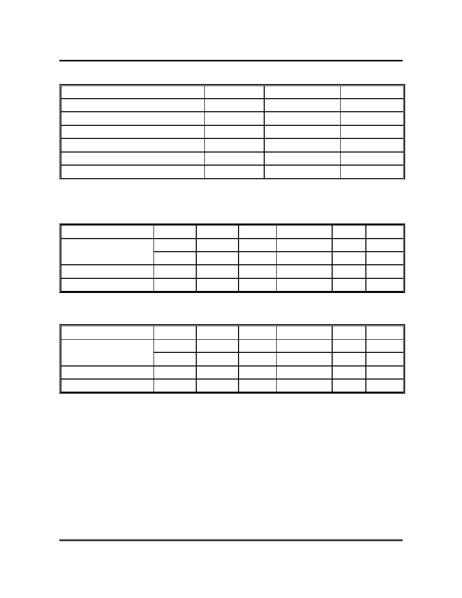
ABSOLUTE MAXIMUM RATINGS
Parameter
Symbol
Value
Unit
Voltage on Any Pin Relative To Vss
VT
-0.5 to 4.6
V
Supply Voltage Relative To Vss
Vcc
-0.5 to 4.6
V
Short circuit Output Current
Iout
50
mA
Power Dissipation
PT
1
W
Operating Temperature
TOPR
0 to 70
∞
C
Storage Temperature
Tstg
-55 to 125
∞
C
RECOMMENDED DC OPERATING CONDITIONS
(Ta = 0 to +70
∞∞
C
) For T2316405A-10 only
Parameter
Symbol
Min.
Typ
Max.
Unit
Notes
Vss
0
0
0
V
Supply Voltage
Vcc
2.4
2.6
2.8
V
1
Input High Voltage
VIH
2.0
-
Vcc+0.3V
V
1
Input Low Voltage
VIL
-0.3
-
0.8
V
1
(Ta = 0 to +70
∞∞
C
) For T2316407A-50/60/70 only
Parameter
Symbol
Min.
Typ
Max.
Unit
Notes
Vss
0
0
0
V
Supply Voltage
Vcc
3.0
3.3
3.6
V
1
Input High Voltage
VIH
2.0
-
Vcc+0.3V
V
1
Input Low Voltage
VIL
-0.3
-
0.8
V
1
Notes : 1. All voltages referenced to Vss
TE
CH
tm
Preliminary T2316407A
Taiwan Memory Technology, Inc. reserves the right
P. 4
Publication Date: APR. 2001
to change products or specifications without notice.
Revision:0.B
T2316405A
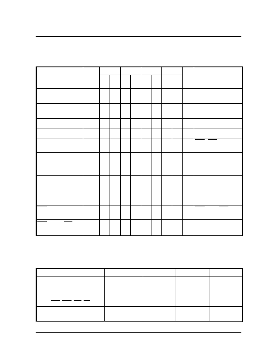
DC CHARACTERISTICS
(Ta = 0 to 70
∞∞
C
) T2316405A-10 Vcc = 2.6V
±
0.2V, Vss = 0V
T2316407A-50/60/70 Vcc = 3.3V
±
0.3V, Vss = 0V
-50
-60
-70
-10
Parameter
Symbol Min Ma
x
Min Ma
x
Min Ma
x
Min Ma
x
Unit
Test Condition
Input Leakage Current
ILI
-5 5
-5 5
-5 5 -5 5 uA
0V
Vin
Vcc+ 0.3V
Other pins = 0V
Output Leakage
Current
ILO -5 5 -5 5 -5 5 -5 5 uA
0V
Vout
Vcc
Dout = disable
Output High Voltage
VOH 2.0 - 2.0 - 2.0 - 2.0 - V High Iout= -2.0mA
Output Low Voltage
VOL - 0.8 - 0.8 - 0.8 - 0.8 V Low Iout=2.0mA
Operating Current
Icc1
-
95 -
90 -
80 -
50 mA
RAS
,
CAS
cycling
tRC=min
Standby Current
Icc2
-
2
-
2
-
2
-
2 mA
TTL interface,
RAS ,CAS =VIH,
DOUT=High-Z
Standby Current
Icc3
- 0.5 - 0.5 - 0.5 - 0.5 mA
CMOS interface,
RAS , CAS > Vcc-0.2V
EDO Page Mode
Current
Icc4
-
95 -
90 -
80 -
50 mA RAS =VIL,CAS
cycling, tPC= min
RAS -only refresh
Current
Icc5
-
95 -
90 -
80 -
50 mA
CAS =VIH, RAS
cycling,
t
RC
= min
CAS Before RAS
Refresh Current
Icc6
-
95 -
90 -
80 -
50 mA
RAS
,
CAS
cycling,
tRC= min
Note: Icc depends on output load condition when the device is selected.
Icc max is specified at the output open condition, Icc is specified as an average current.
CAPACITANCE
(Ta =25
∞
C, f = 1M HZ, T2316405A-10 Vcc = 2.6V, T2316407A-50/60/70 Vcc = 3.3V)
Parameter
Symbol
Typ
Max
Unit
Input Capacitance
(address)
CI1
-
5
pF
Input Capacitance
( RAS ,CAS ,WE ,OE )
CI2
-
7
pF
Output Capacitance
(data-in/out)
CI/O
-
7
pF
TE
CH
tm
Preliminary T2316407A
Taiwan Memory Technology, Inc. reserves the right
P. 5
Publication Date: APR. 2001
to change products or specifications without notice.
Revision:0.B
T2316405A
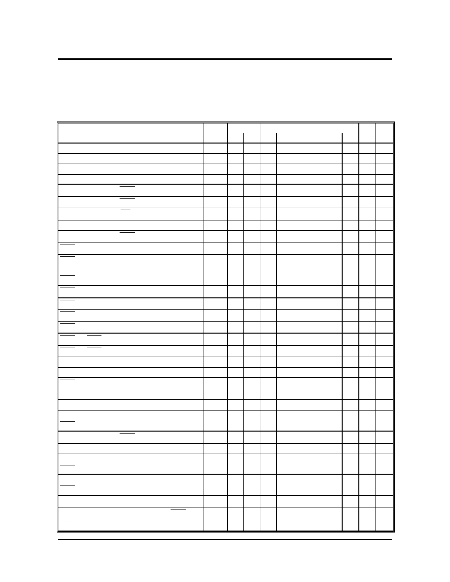
AC CHARACTERISTICS
(note 1,2,3) (Ta = 0 to 70
∞
C)
TEST CONDITIONS:
T2316405A-10 Vcc = 2.6V
±
0.2V , T2316407A-50/60/70 Vcc = 3.3V
±
0.3V
V
IH
/V
IL
=2.0/0.8V,V
OH
/V
OL
=2.0/0.8V
Input rise and fall times: 2ns , Output Load: 2TTL gate + CL (100pF)
-50
-60
-70
-10
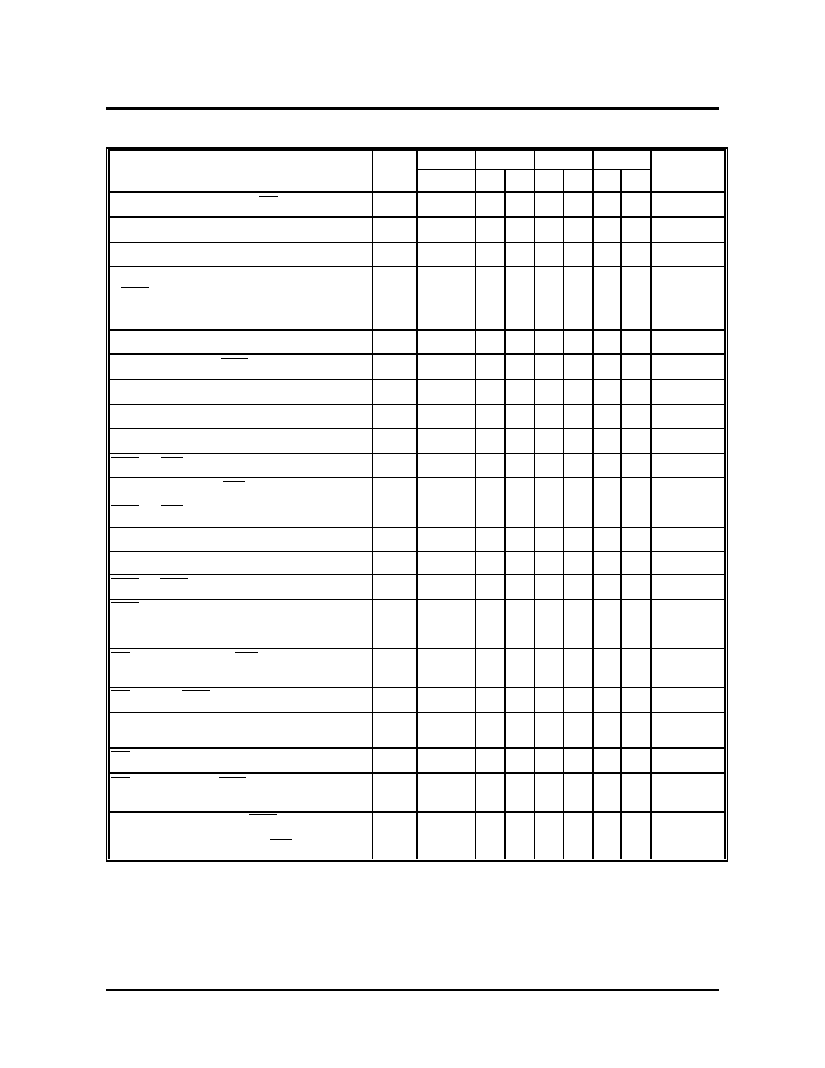
AC CHARACTERISTICS
PARAMETER
SYM
Min Max Min Max Min Max Min Max
UNIT
Notes
Read or Write Cycle Time
tRC
84
104 124 180
ns
Read Write Cycle Time
tRWC 108 135 160 240 ns
EDO-Page-Mode Read or Write Cycle Time tPC
20
25
30
40
ns
EDO-Page-Mode Read-Write Cycle Time
tPCM 56 68 78 120 ns
Access Time From RAS
tRAC 50 60 70 100 ns 4
Access Time From CAS
tCAC 13 15 20 25 ns 5
Access Time From OE
tOAC 13 15 20 25 ns 13
Access Time From Column Address
tAA
25
30
35
50 ns 8
Access Time From
CAS
Precharge
tACP
30
35
40
55 ns
RAS Pulse Width
tRAS 50 10K 60 10K 70 10K 100 10K ns
RAS Pulse Width (EDO Page Mode)
tRASC 50 100
K
60 100
K
70 100
K
100 100
K
ns
RAS Hold Time
tRSH 8
10
13
25
ns
RAS Precharge Time
tRP
30
40
50
70
ns
CAS
Pulse Width
tCAS 8 10K 10 10K 13 10K 25 10K ns
CAS Hold Time
tCSH 38 40 45 100 ns
CAS
Precharge Time (EDO Page Mode)
tCP
10
10
10
10
ns
RAS to CAS Delay Time
tRCD 12 37 14 45 14 50 25 75 ns 7
CAS to RAS Precharge Time
tCRP 5
5
5
5
ns
Row Address Setup Time
tASR 0
0
0
0
ns
Row Address Hold Time
tRAH 8
10
10
15
ns
RAS to Column Address Delay Time
tRAD 10 25 12 30 12 35 20 50 ns 8
Column Address Setup Time
tASC 0
0
0
0
ns
Column Address Hold Time
tCAH 8
10
13
20
ns
Column Address Hold Time (Reference to
RAS )
tAR
21
24
27
45
ns
Column Address to RAS Lead Time
tRAL 25 30 35 50 ns
Read Command Setup Time
tRCS 0
0
0
0
ns 14
Read Command Hold Time Reference to
CAS
tRCH 0 0 0 0 ns 9,14
Read Command Hold Time Reference to
RAS
tRRH 0 0 0 0 ns 9
CAS
to Output in Low-Z
tCLZ 0
0
0
0
ns
Output Buffer Turn-off Delay From CAS or
RAS
tOFF1
0 12 0 15 0 20 0 25 ns
10,16
TE
CH
tm
Preliminary T2316407A
Taiwan Memory Technology, Inc. reserves the right
P. 6
Publication Date: APR. 2001
to change products or specifications without notice.
Revision:0.B
T2316405A
AC CHARACTERISTICS
(continued)
-50
-60
-70
-10
AC CHARACTERISTICS
PARAMETER
SYM
Min Max Min Max Min Max Min Max
UNIT
Notes
Output Buffer Turn-off to OE
tOFF2
0 12 0 15 0 20 0 25 ns 16
Write Command Setup Time
tWCS 0
0
0
0
ns 11,14
Write Command Hold Time
tWCH 8
10
13
15
ns
Write Command Hold Time (Reference
toRAS )
tWCR 21 24 27 40 ns 14
Write Command Pulse Width
tWP
8
10
10
15
ns 14
Write Command to RAS Lead Time
tRWL 10 10 13 25
ns 14
Write Command to CAS Lead Time
tCWL 8 10 13 25 ns 14
Data-in Setup Time
tDS
0
0
0
0
ns 12
Data-in Hold Time
tDH
8
10
13
20
ns 12
Data-in Hold Time (Reference to RAS )
tDHR 21 24 27 45 ns
RAS
to
WE
Delay Time
tRWD 64 79 94 130
ns 11
Column Address to WE Delay Time
tAWD 39 49 59 80 ns 11
CAS to WE Delay Time
tCWD 26 34 44 55 ns 11
Transition Time (rise or fall)
tT
2 50 2 50 2 50 2 50 ns 2,3
Refresh Period (2048 cycles)
tREF 32
32
32
32 ms
RAS
to
CAS
Precharge Time
tRPC 5
5
5
5
ns
CAS Setup Time (CBR REFRESH)
tCSR 5 10 10 10 ns 6
CAS Hold Time (CBR REFRESH)
tCHR 8 10 10 10 ns 6
OE Hold Time From WE During Read-
Modify-Write Cycle
tOEH 8 10 13 25 ns 15
OE Low to CAS High Setup Time
tOES 5
5
5
5
ns
OE
High Hold Time From
CAS
High
tOEH
C
5
5
5
5
ns
OE High Pulse Width
tOEP 10 10 10 10 ns
OE
Setup Prior to
RAS
During Hidden
Refresh Cycle
tORD 5 7 10 13 ns
Data Output Hold After CAS Returning Low tCOH 5
5
5
5
ns
Output Disable Delay From WE
tWHZ 10 15 20 25 ns

TE
CH
tm
Preliminary T2316407A
Taiwan Memory Technology, Inc. reserves the right
P. 7
Publication Date: APR. 2001
to change products or specifications without notice.
Revision:0.B
T2316405A
Notes:
1. An initial pause of 200us is required after
power-up followed by eight RAS refresh
cycles ( RAS only or CBR) before proper
device operation is assured. The eight
RAS
cycle wake -ups should be repeated any time
the tREF refresh requirement is exceeded.
2. VIH(2.0V) and VIL(0.8V) are reference
levels for measuring timing of input signals.
Transition times are measured between
VIH(2.0V) and VIL(0.8V).
3. In addition to meet the transition rate
specification, all input signals must transit
between VIH and VIL in a monotonic manner.
4. Assume that tRCD < tRCD(max). If tRCD is
greater than the maximum recommended value
shown in this table, tRAC will increase by the
amount that tRCD exceeds the value shown.
5. Assume that tRCD
tRCD(max) .
6. Enables on-chip refresh and address counters.
7. Operation within the tRCD(max) limit ensures
that tRAC(max) can be met. tRCD(max) is
specified as a reference point only; if tRCD is
greater than the specified tRCD(max) limit,
access time is controlled by tCAC.
8. Operation within the tRAD limit ensures that
tRAC(max) can be met. tRAD(max) is
specified as a reference point only; if tRAD is
greater than the specified tRAD(max) limit,
access time is controlled by tAA.
9. Either tRCH or tRRH must be satisfied for a
READ cycle.
10. tOFF1(max) defines the time at which the
output achieves the open circuit condition; it is
not a reference to VOH or VOL.
11. tWCS, tRWD, tAWD and tCWD are
restrictive operating parameters in LATE
WRITE and READ-MODIFY -WRITE cycles
only. If tWCS
tWCS(min), the cycle is an
EARLY WRITE cycle and the data output will
remain an open circuit throughout the entire
cycle. If tRWD
tRWD(min), tAWD
tAWD(min) and tCWD
tCWD(min), the
cycle is READ-WRITE and the data output
will contain data read from the selected cell. If
neither of the above conditions is met, the state
of I/O (at access time and until CAS and
RAS
or
OE
go back to VIH) is indeterminate.
OE held high and WE taken low after CAS
goes low result in a LATE WRITE (OE -
controlled) cycle.
12. These parameters are referenced to CAS
leading edge in EARLY WRITE cycles and
WE
leading edge in LATE WRITE or READ-
MODIFY-WRITE cycles.
13. During a READ cycle, if
OE
is low then taken
HIGH before CAS goes high, I/O goes open,
if OE is tied permanently low, a LATE
WRITE or READ-MODIFY-WRITE
operation is not possible.
14. WRITE command is defined as WE going low.
15. LATE WRITE and READ-MODIFY-WRITE
cycles must have both tOFF2 and tOEH met
(
OE
high during WRITE cycle) in order to
ensure that the output buffers will be open
during the WRITE cycles.
16. The I/Os open during READ cycles once
tOFF1 or tOFF2 occur.
TE
CH
tm
Preliminary T2316407A
2
Taiwan Memory Technology, Inc. reserves the right
P. 8
Publication Date: APR. 2001
to change products or specifications without notice.
Revision:0.B
T2316405A
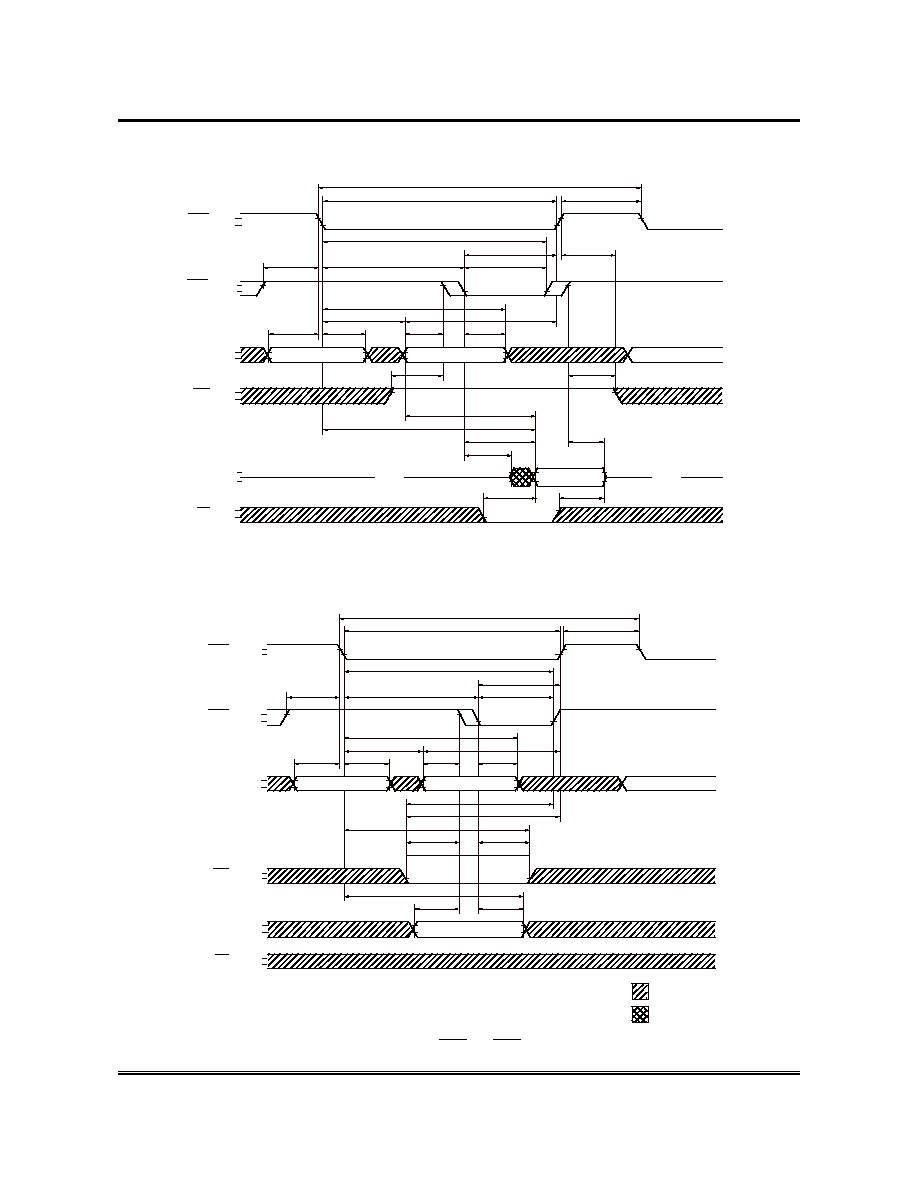
READ CYCLE
RA S
CA S
VIH
V IL
VOH
VOL
VIH
VIL
VIH
VIL
VIH
VIL
VIH
VIL
A DDR
WE
OE
I/O
t R A S
tR C
t R P
V A L ID D A T A
C O L U M N
R O W
R O W
tA S R
t R A H
tR A D
tC R P
t C S H
t R AL
tA S C
t C A H
tO F F 1
N O T E 1
t R R H
tA R
tA A
t C AC
t C L Z
t R AC
O P E N
O P E N
tO F F 2
tO A C
t R S H
t C A S
tR C D
tR C S
t RC H
EARLY WRITE CYCLE
RAS
C AS
V IH
V IL
V IOH
V IOL
V IH
V IL
V IH
V IL
V IH
V IL
V IH
V IL
A DDR
WE
OE
I/O
tR A S
tR C
tR P
V A L ID D A T A
C O L U M N
R O W
R O W
tA S R
tR A H
tR A D
tC R P
tC S H
tC W L
tR W L
tW C R
tA R
tD H R
tW P
t D S
tD H
tR S H
t C A S
t RC D
tW C H
tA S C
t C A H
t R A L
t WC S
DON'T CARE
UNDEFINED
Note: t
OFF1
is referenced from the rising edge of
RAS
or
CAS
, whichever occurs last.
TE
CH
tm
Preliminary T2316407A
2
Taiwan Memory Technology, Inc. reserves the right
P. 9
Publication Date: APR. 2001
to change products or specifications without notice.
Revision:0.B
T2316405A
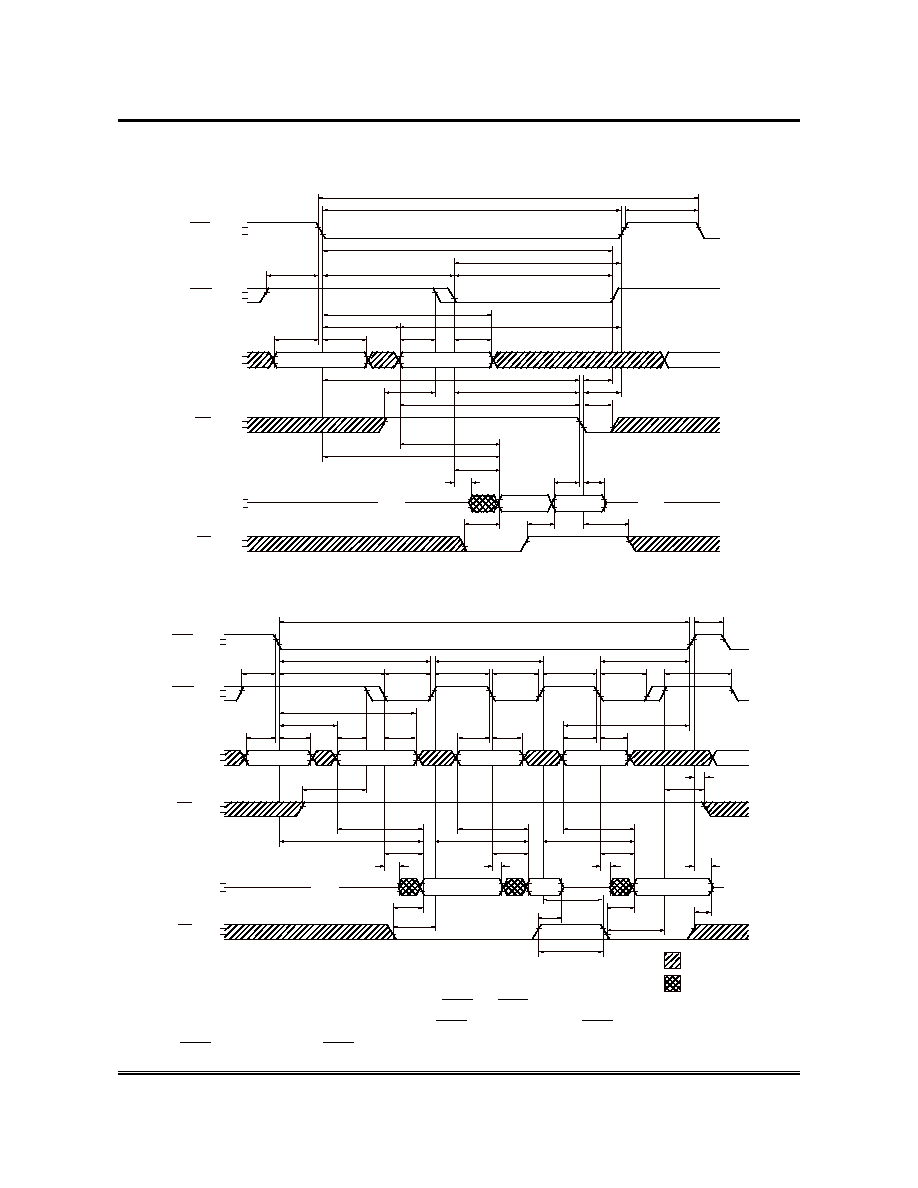
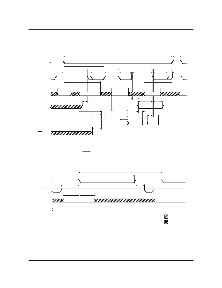
READ WRITE CYCLE
(LATE WRITE and READ-MODIFY-WRITE CYCLES)
RA S
CA S
VIH
V IL
VIOH
V IOL
VIH
V IL
VIH
V IL
VIH
V IL
VIH
V IL
ADDR
WE
OE
I/O
tR A S
tR WC
tR P
V A LID D
O U T
C O L U M N
R O W
R O W
tA S R
tR A H
tR AD
tC R P
tC S H
tR AL
tA S C
tC A H
tA R
tA A
tC AC
tC L Z
tR A C
O P E N
O P E N
tOF F 2
tOA C
tR S H
tC A S
tRC D
tR C S
tOE H
V A L ID D
IN
t DH
tD S
tR WD
tC WD
tA WD
tC WL
tR WL
tWP
EDO-PAGE-MODE READ CYCLE
RAS
CA S
VIH
VIL
VOH
VOL
VIH
VIL
VIH
VIL
VIH
VIL
VIH
VIL
ADDR
WE
OE
I/O
t R P
V A L ID
D A T A
C O L U MN
R O W
R O W
t A S R
t R A H
t R A D
t C R P
t R A L
t A S C
t C A H
t A R
t A A
t C A C
t C L Z
t R A C
O P E N
O P E N
t O F F 2
t O A C
t C S H
t R C D
t R C S
t O E H C
DON'T CARE
UNDEF INED
t R A S C
t C P N
t R S H
t C P
t P C
t C P
t C A S
C O L U M N
t A S C
t C A H
t A S C
t C A H
C O L U M N
V A LID
DA T A
t C O H
t C L Z
t A A
t C A C
t A A
t C A C
t O E P
t O E S
t O F F 2
t O A C
t O E S
t O F F 1
N O T E 1
t A C P
t A C P
t R R H
t R C H
t C A S
t C A S
V A L ID
D A T A
Note: 1. t
OFF1
is referenced from the rising edge of
RAS
or
CAS
, whichever occurs last.
2. t
PC
can be measured from falling edge of CAS to falling edge of CAS , or from rising edge of
CAS to rising edge of CAS . Both measurements must meet the t
PC
specification.
TE
CH
tm
Preliminary T2316407A
2
Taiwan Memory Technology, Inc. reserves the right
P.10
Publication Date: APR. 2001
to change products or specifications without notice.
Revision:0.B
T2316405A
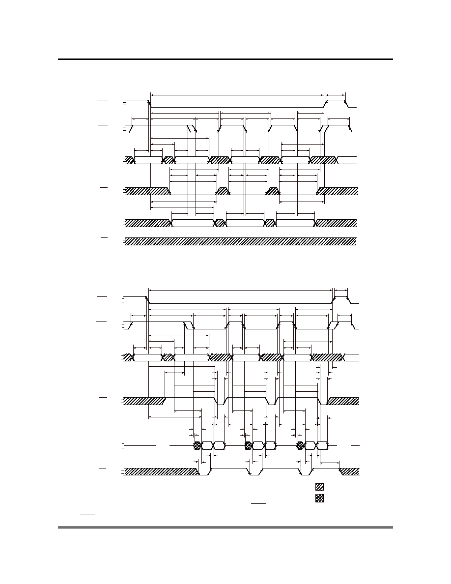
EDO-PAGE-MODE EARLY-WRITE CYCLE
RAS
CA S
VIH
VIL
VIOH
VIOL
VIH
VIL
VIH
VIL
VIH
VIL
VIH
VIL
ADDR
WE
OE
I/O
V A L ID D A T A
t C A S
t R C D
t C R P
t C S H
t P C
t C P
t C P
t R S H
t C P N
t R A S C
V A L ID D A T A
VA LID DA TA
C O LU MN
C O L U MN
C O L U MN
RO W
RO W
t A S R t R A H
t R A D
t A R
t A S C
t C A H
t A S C t C A H
t A S C t C A H
t R A L
t W C S
t W C H
t C W L
t W P
t W C S
t C W L
t W C H
t W P
t W C S
t C W L
t W C H
t W P
t D S
t W C R
t D H R
t D H
t D S
t D H
t D S
t D H
t R W L
t C A S
t C A S
EDO-PAGE-MODE READ-WRITE CYCLE
(LATE WRITE and READ-MODIFY-WRITE CYCLES)
VIOH
VIOL
VIH
VIL
OE
I/O
t D H
t C A C
t C L Z
O P E N
O P E N
t O F F 2
t O A C
D ON 'T CAR E
UNDEF INED
t A A
t O E H
t O F F 2
t O A C
t A C P
RAS
CAS
VIH
VIL
VIH
VIL
VIH
VIL
VIH
VIL
ADDR
WE
t R P
C O L U M N
RO W
RO W
t A S R t R A H
t R A D
t C R P
t R A L
t A S C
t C A H
t A R
t A A
t D S
t R A C
t C S H
t C A S
t R C D
t R C S
t R A S C
t C P N
t R S H
t C P
t C P
t C A S
t C A S
C O L U M N
t A S C t C A H
t A S C t C A H
C O L U M N
t A A
t A C P
t R W L
t C W L
t W P
t C W L
t W P
t R W D
t A W D
t C W D
t C W D
t A W D
t C W D
t A W D
t C W L
t W P
t O F F 2
t O A C
t D H
t D S
t DH
t DS
t C A C
t C L Z
t C A C
t C L Z
t P C M
VAL ID
DIN
VALI D
DO UT
VALI D
DIN
V ALI D
DOUT
V ALI D
DIN
VALI D
DOUT
Note: t
PC
can be measured from falling edge to falling edge of CAS , or from rising edge to rising edge of
CAS . Both measurements must meet the t
PC
specification.
TE
CH
tm
Preliminary T2316407A
2
Taiwan Memory Technology, Inc. reserves the right
P.11
Publication Date: APR. 2001
to change products or specifications without notice.
Revision:0.B
T2316405A
EDO-PAGE-MODE READ-EARLY-WRITE CYCLE
(Pseudo READ-MODIFY-WRITE)
RAS
CA S
VIH
V IL
VIO H
VIOL
VIH
V IL
VIH
VIL
VIH
V IL
VIH
VIL
ADDR
WE
OE
I/O
t R P
V A L ID
D A T A ( B )
R O W
R O W
tA S R t R A H
tR A D
t C R P
tC S H
tR A L
t AS C
tC A H
tR A S C
tR S H
tA R
tA A
t C A C
t R AC
O P E N
t OA C
t P C
t C A S
tR C D
tR C S
C O L U M N ( A )
C O L U M N ( B )
C O L U M N (N )
VALID DATA
IN
V A L ID D A T A ( A )
t C P
t P C
tC P
tC A S
tC A S
t C P
tA S C
tC A H
t AS C
tC A H
tWC H
tW C S
tR C H
tA A
tC A C
tC O H
tA C P
tD S
tD H
t WH Z
RAS ONLY REFRESH CYCLE
(ADDR=A0-A10;
O E
,
WE
=DON`T CARE)
RAS
CA S
VIH
VIL
V OH
V OL
VIH
VIL
VIH
VIL
ADDR
I/O
tR A S
t RC
tR P
O P E N
R O W
R O W
t A S R
tR A H
t C R P
tR P C
DON'T CARE
UNDEFINED
TE
CH
tm
Preliminary T2316407A
Taiwan Memory Technology, Inc. reserves the right
P. 12
Publication Date: APR. 2001
to change products or specifications without notice.
Revision:0.B
T2316405A
CBR REFRESH CYCLE
(A0-A10; OE =DON`T CARE)
R A S
C A S
V I H
V IL
V I H
V IL
V I H
V IL
I/O
t R A S
t R A S
t R P
O P E N
t R P C
t C P N
WE
t R P
t C S R
t C H R
t R P C
t C S R
t C H R
t W R P t W R H
t W R P t W R H
HIDDEN REFRESH CYCLE
(
WE =HIGH;OE =LOW)
R A S
C A S
V IH
V IL
V OH
V O L
V IH
V IL
V IH
V IL
I /O
( R E F R E S H )
t R A S
t R P
O P E N
V A L I D D A T A
t C R P
O E
O P E N
V IH
V IL
A D D R
R O W
t A S R
t R A H
t R A D
t R A L
t A S C
t C A H
t A R
t A A
t C A C
t C L Z
t R A C
t O A C
t R S H
t R C D
t C H R
C O L U M N
t O F F 2
tORD
t O FF 1
N O T E 1
( R E A D )
t R A S
Note: 1. t
OFF1
is referenced from the rising edge of
RAS
or
CAS
, whichever occurs last.
TE
CH
tm
Preliminary T2316407A
Taiwan Memory Technology, Inc. reserves the right
P. 13
Publication Date: APR. 2001
to change products or specifications without notice.
Revision:0.B
T2316405A
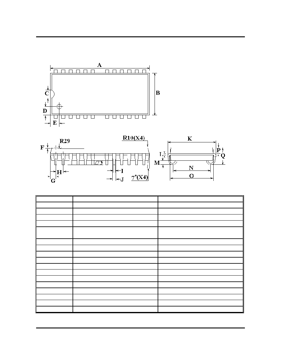
PACKAGE DIMENSIONS
24-LEAD SOJ DRAM (300 mil)
SYMBOL
DIMENSIONS IN INCHES
DIMENTIONS IN MM
A
0.673±0.002
17.09±0.05
B
0.300±0.002
7.62±0.13
C
0.060±0.002
1.52±0.05
D
0.050±0.001
1.27±0.03
E
0.063±0.001
1.63±0.03
F
0.015±0.002
0.38±0.05
G
0.036±0.002
0.91±0.05
H
0.050±0.002
1.27±0.05
I
0.018±0.002
0.46±0.05
J
0.028±0.002
0.71±0.05
K
0.336±0.003
8.53±0.08
L
0.010±0.001
0.25±0.03
M
0.029±0.002
0.74±0.05
N
0.268±0.003
6.81±0.08
O
0.300±0.002
7.62±0.05
P
0.042±0.001
1.07±0.03
Q
0.129±0.004
3.28±0.10
y
0.004(MAX)
0.102(MAX)
TE
CH
tm
Preliminary T2316407A
Taiwan Memory Technology, Inc. reserves the right
P. 14
Publication Date: APR. 2001
to change products or specifications without notice.
Revision:0.B
T2316405A
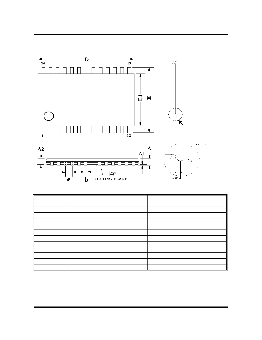
PACKAGE DIMENSIONS
24-LEAD TSOP II DRAM (300 mil)
SYMBOL
DIMENSIONS IN INCHES
DIMENTIONS IN MM
A
0.047(MAX)
1.20(MAX)
A1
0.004±0.002
0.10±0.05
A2
0.039±0.002
1.00±0.05
b
0.016±0.004
0.41±0.11
D
0.675±0.005
17.14±0.13
E
0.368±0.003
9.22±0.20
E1
0.300±0.005
7.62±0.13
e
0.050
1.27
L'
0.020±0.004
0.50±0.10
L1'
0.031
0.80
y
0.002±0.002
0.05±0.05
1
∞
~ 5
∞
1
∞
~ 5
∞
"A"