
TE
CH
tm
T62M0001A
TM Technology Inc. reserves the right P. 1 Publication Date: JUN. 2002
to change products or specifications without notice. Revision:A
T62M0001A
Digital Sound Processor
With 64K SRAM
Features
l Low Noise (-90dBV typical)
l Low Distortion (0.17% typical)
l Built ≠in 64 K SRAM
l Sleep Mode Function
l Two Control Modes Selection:
Easy Mode Using Parallel Data
u-COM Mode Using Serial Data
l Auto-Mute Function
l Built-in Automatic Reset Circuit
l Pin Compatible with M65831
Description
T62M0001 is a digital echo/surround processor
IC utilizing CMOS technology. Analog signal
to T62M0001 is digitized by a built-in A/D
converter and then stored in the internal
memory. After an adjustable delay time, data in
the memory is read and converted back to
analog signal via the other D/A converter. With
the built-in 64K SRAM, T62M0001 can create
very high performance echo/surround sound
effect and meet the application of A/V system
such as CD player VCD,DVD ....etc.
Part Number Examples
Part NO.
Pkg
Description
T62M0001A-D
24-SOP
24-SOP
T62M0001A-K
24-DIP
600mil-24-DIP

TE
CH
tm
T62M0001A
TM Technology Inc. reserves the right P. 2 Publication Date: JUN. 2002
to change products or specifications without notice. Revision:A
Pin Configuration
c
V
DD
1
24 V
CC
XIN
2
23 LPF1 IN
XOUT
3
22 LPF1 OUT
D1/REQ
4
21 OP1 OUT
D2/SCK
5
20 OP1 IN
D3/DATA
6
19 REF
D4/IDSW
7
18 CC1
TEST
8
17 CC2
EASY/u-COM
9
16 OP2 IN
SLEEP
10
15 OP2 OUT
D-GND
11
14 LPF2 IN
A-GND
12
13 LPF2 OUT
24 PINS DIP/SOP
TE
CH
tm
T62M0001A
TM Technology Inc. reserves the right P. 3 Publication Date: JUN. 2002
to change products or specifications without notice. Revision:A
Pin Description
Symbol
I/O
Function
Pin no.
V
DD
P Digital supply voltage
1
XIN
I Oscillator input
2
XOUT
O Oscillator output
3
D1/REQ
I
Easy mode : inputs D1 data
u
-COM mode :inputs request data
4
D2/SCK
I
Easy mode : inputs D2 data
u
-COM mode : inputs shift clock
5
D3/DATA
I
Easy mode : inputs D3 data
u
-COM mode : inputs serial data
6
D4/IDSW
I
Easy mode : inputs D4 data
u
-COM mode : controls ID code
7
TEST
I L = normal mode
8
EASY/
u
-COM I
H = easy mode
L =
u
-COM mode
9
SLEEP
I H = sleep mode
L = normal mode
10
D-GND
G Digital ground
11

TE
CH
tm
T62M0001A
TM Technology Inc. reserves the right P. 4 Publication Date: JUN. 2002
to change products or specifications without notice. Revision:A
Symbol
I/O
Function
Pin no.
A-GND
G Analog ground
12
LPF2 OUT
O Low pass filter 2 output
13
LPF2 IN
I Low pass filter 2 input
14
OP2 OUT
O Integrator 2 output
15
OP2 IN
I Integrator 2 input
16
CC2
- Current control 2
17
CC1
- Current control 1
18
REF
- Analog reference voltage ( = 1/2 V
CC
)
19
OP1 IN
I Integrator 1 input
20
OP1 OUT
I Integrator 1 output
21
LPF1 OUT
- Low pass filter 1 output
22
LPF1 IN
O Low pass filter 1 input
23
V
CC
P Analog supply voltage
24
P : supply voltage
G : ground
I : input pin
O : output pin

TE
CH
tm
T62M0001A
TM Technology Inc. reserves the right P. 5 Publication Date: JUN. 2002
to change products or specifications without notice. Revision:A
Function description
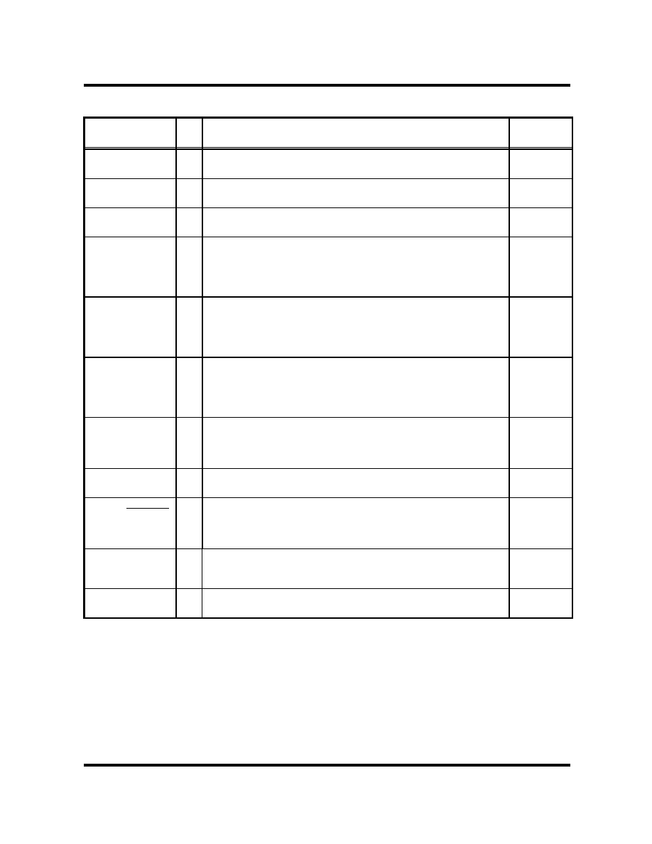
1.Easy mode (parallel data input)
When the pin EASY/
COM
-
µ
= "High", then in the easy mode.
D4
D3
D2
D1
fs
Td
L
L
L
L
Fck/3
12.3
L
L
L
H
Fck/3
24.6
L
L
H
L
Fck/3
36.9
L
L
H
H
Fck/3
49.2
L
H
L
L
Fck/3
61.4
L
H
L
H
Fck/3
73.7
L
H
H
L
Fck/3
86.0
L
H
H
H
Fck/3
98.3
H
L
L
L
Fck/6
110.6
H
L
L
H
Fck/6
122.9
H
L
H
L
Fck/6
135.2
H
L
H
H
Fck/6
147.5
H
H
L
L
Fck/6
159.7
H
H
L
H
Fck/6
172.0
H
H
H
L
Fck/6
184.3
H
H
H
H
Fck/6
196.6
Note : f s : sampling frequency (Hz) ; Fck : oscillator frequency(example Fck=2MHz)
Td : delay time (msec)
TE
CH
tm
T62M0001A
TM Technology Inc. reserves the right P. 6 Publication Date: JUN. 2002
to change products or specifications without notice. Revision:A
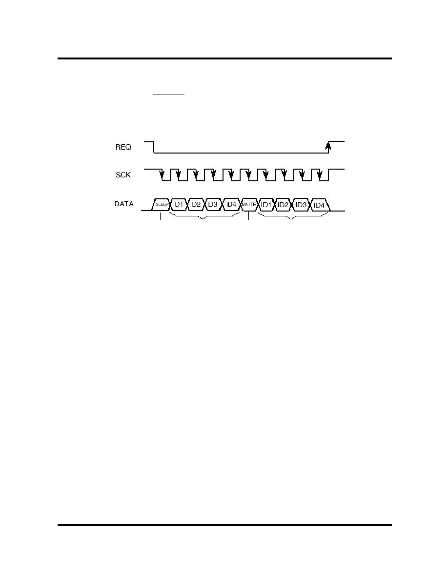
2.u-COM mode (serial data input)
When the pin EASY/
COM
u
-
= "Low" , then in the u-COM mode.
The timing is shown as the diagram below:
H Delay time H ID code
= Sleep mode = Mute
This timing chart shows that delay time is set by serial data from u-COM.
DATA signal is latched at the falling edge of SCK signal, the last ten datas are set at the rising edge
of REQ signal when ID codes are satisfied.
ID1, ID3 =
Low
ID2
=
High
ID4
= Equal to IDSW

TE
CH
tm
T62M0001A
TM Technology Inc. reserves the right P. 7 Publication Date: JUN. 2002
to change products or specifications without notice. Revision:A
REQ, SCK, DATA input timing
Symbol
Parameter
Limits
Unit
Min.
Typ.
Max.
t1
SCK pulse width
250
-
-
ns
ds
SCK pulse duty
-
50
-
%
t2
DATA setup time
100
t1/2
-
ns
t3
DATA hold time
100
t1/2
-
ns
t4
REQ hold time
100
-
-
ns
t5
REQ pulse width
250
-
-
ns

TE
CH
tm
T62M0001A
TM Technology Inc. reserves the right P. 8 Publication Date: JUN. 2002
to change products or specifications without notice. Revision:A
3.Mute
(1) Easy mode
Automatic mute upon changing delay time, cancelling SLEEP mode and power on.
(2) u-COM
MUTE=H : mute.
MUTE=L : automatic mute.
Automatic mute :
Delay signal before change mode Delay signal after change mode
(a) Upon changing delay time
Delay signal
(b) Upon cancel sleep mode
Delay signal
Power on
(c) Upon power on

TE
CH
tm
T62M0001A
TM Technology Inc. reserves the right P. 9 Publication Date: JUN. 2002
to change products or specifications without notice. Revision:A
4.SLEEP mode
SLEEP data is :
H=clock and RAM stop to reduce circuit current (SLEEP mode)
L=normal operation
5.System reset
Automatically reset power-on. The reset time is about 120 m second.
Delay time is set at 147.5 m second.
TE
CH
tm
T62M0001A
TM Technology Inc. reserves the right P. 10 Publication Date: JUN. 2002
to change products or specifications without notice. Revision:A
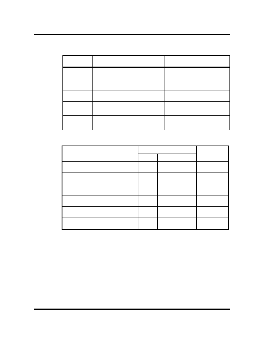
Absolute maximum rating (Ta=25∫C,unless otherwise noted)
symbol
paramatic
ratings
unit
Vcc
Supply voltage
6
V
Icc
Circuit current
100
mA
Pd
Power dissipation
1.7
W
Topr
Operating temperature
-20~75
∫C
Tstg
Storage temperature
-25~125
∫C
Recommended operating conditions
rating
symbol
parameter
Min.
Typ.
Max.
unit
V
CC
Supply voltage
4.5
5
5.5
V
V
DD
Supply voltage
4.5
5
5.5
V
V
CC
-V
DD
Difference voltage
-0.3
0
0.3
V
fck
Clock frequency
1
2
3
MHz
V
IH
"H" input voltage
0.7V
DD
-
-
V
V
IL
"L" input voltage
-
-
0.3V
DD
V

TE
CH
tm
T62M0001A
TM Technology Inc. reserves the right P. 11 Publication Date: JUN. 2002
to change products or specifications without notice. Revision:A
Electrical characteristics
(Vcc=5.0V,fin=1KHz,Vi=100mVrms,f
ck
=2MHz,Ta=25
∫C
, unless otherwise noted)
symbol
Parameter
Test condition
Min.
Typ. Max.
unit
Icc
Circit current
No signal
-
13
20
mA
Gv
Voltage gain
R
L
=47K
-
-0.5
2.5
dB
Iccs
Circit current
(Sleep Mode)
Sleep Mode
-
7
10
mA
Vomax
Max. output voltage
THD=10%
1.3
1.6
-
Vrms
fs=666KHz
-
0.17
0.6
%
THD
Output distorton
30KHz
L.P.F.
fs=333KHz
-
0.4
1.0
%
Upon changing delay time
508
528
548
ms
TMUTE
Mute time
Upon canceling sleep mode
508
528
548
ms
No
Output noise voltage
DIN-AUDIO(fs=666KHz)
-
-90
-80
dBV
DC electrical characteristics
limits
symbol
parameter
Min.
Typ.
Max.
unit
Vcc
Supply voltage
4.5
5
5.5
V
Icc
Circuit current
-
13
20
mA
V
IH
"H" input voltage
0.7V
DD
-
-
V
V
IL
"L" input voltage
-
-
0.3V
DD
V

TE
CH
tm
T62M0001A
TM Technology Inc. reserves the right P. 12 Publication Date: JUN. 2002
to change products or specifications without notice. Revision:A
Application circuit
C13
0.1UF
U1
T62M0001A
1
2
3
4
5
6
7
8
9
10
11
12
13
14
15
16
17
18
19
20
21
22
23
24
VDD
XIN
XOUT
D1
D2
D3
D4
TEST
EASY/£g-COM
SLEEP
DGND
AGND
LPF2_OUT
LPF2_IN
OP2_OUT
OP2_IN
CC2
CC1
REF
OP1_IN
OP1_OUT
LPF1_OUT
LPF1_IN
VCC
C5
1UF
R5
30K
AGND
DGND
C17
0.01UF
C4
4700PF
SETING
DELAY
TIMES
C3
100PF
C14
0.01UF
R7
18K
OUT
1
C6
100PF
C12
0.33UF
C10
47UF/10V
R2
20K
R3
18K
R8
3K
C1
100UF/10v
C15
560PF
R9
20K
EASY MODE
R10
2.7K
C16
4700PF
VCC
C11
0.33UF
R1
10K
R6
10K
IN
1
R4
20K
C7
560PF
C2
0.1UF
C18
1UF
SW1
1
2
C8
0.1UF
VCC
C9
1UF
Y1
2MHZ
C9
1UF
C13
0.1UF
SW1
1
2
R3
18K
AGND
VCC
C4 4700PF
U1
T62M0001A
1
2
3
4
5
6
7
8
9
10
11
12
13
14
15
16
17
18
19
20
21
22
23
24
VDD
XIN
XOUT
D1
D2
D3
D4
TEST
EASY/£g-COM
SLEEP
DGND
AGND
LPF2_OUT
LPF2_IN
OP2_OUT
OP2_IN
CC2
CC1
REF
OP1_IN
OP1_OUT
LPF1_OUT
LPF1_IN
VCC
C12
0.33UF
R2
20K
C11
0.33UF
C14
0.01UF
C17
0.01UF
DGND
Y1
2MHZ
C18
1UF
OUT
1
R6
10K
C15
560PF
R4
20K
R9
20K
C6
100PF
C3
100PF
C1
100UF/10v
R10
2.7K
IN
1
u-COM MODE
R1
10K
C8
0.1UF
C5
1UF
R8
3K
C10
47UF/10V
C16
4700PF
VCC
C7
560PF
C2
0.1UF
R5
30K
R7
18K
u-COM

TE
CH
tm
T62M0001A
TM Technology Inc. reserves the right P. 13 Publication Date: JUN. 2002
to change products or specifications without notice. Revision:A
IC package
T62M0001A(24-DIP)
A
A 1
B
B1
B2
B3
C
C1
A 1
D
D1
D2
Dimension in mm
Dimension in inch
Symbol
min.
typ.
max
min.
typ.
max.
A
-
32.26
-
-
1.270
-
A1
13.21
-
14.22
0.520
-
0.560
B
-
-
5.08
-
-
0.20
B1
3.18
-
-
0.125
-
-
B2
-
-
4.57
-
-
0.180
B3
0.51
-
-
0.020
-
-
C
2.24
2.54
2.84
0.088
0.100
0.112
C1
4.06
4.57
5.08
0.16
0.18
0.20
D
14.99
-
15.49
0.59
-
0.61
D1
-
0~15∞
-
-
0~15∞
-
D2
-
0.25
-
-
0.01
-

TE
CH
tm
T62M0001A
TM Technology Inc. reserves the right P. 14 Publication Date: JUN. 2002
to change products or specifications without notice. Revision:A
T62M0001A(24-SOP)
D
E 1
E
A
L '
L 1 '
b
Y
1
1 2
1 3
2 4
A
A 1
e
A 2
S C A L E : " A "
Z
C
. . . . .
. . . . .
. . . . .
Dimension in mm
Dimension in inch
Symbol
min.
typ.
max
min.
typ.
max.
A
-
-
2.4
-
-
0.0945
A1
0.05
-
-
0.002
-
-
A2
-
2.0
-
-
0.0787
-
b
0.35
0.4
0.5
0.0138
0.0157
0.0197
C
0.13
0.15
0.2
0.0051
0.0059
0.0079
D
14.8
15.0
15.2
0.5827
0.5906
0.5984
E
8.2
8.4
8.6
0.3228
0.3307
0.3386
e
-
1.27
-
-
0.05
-
E1
11.63
11.93
12.23
0.4579
0.4697
0.4815
L
0.3
0.5
0.7
0.0118
0.0197
0.0276
L1
-
1.7650
-
-
0.0448
-
Y
-
-
0.15
-
-
0.0059
0∞
-
10∞
0∞
-
10∞