 | –≠–ª–µ–∫—Ç—Ä–æ–Ω–Ω—ã–π –∫–æ–º–ø–æ–Ω–µ–Ω—Ç: T63H0006B | –°–∫–∞—á–∞—Ç—å:  PDF PDF  ZIP ZIP |
TE
CH
tm
T63H0006B
TM Technology Inc. reserves the right P. 1 Publication Date: JUN. 2004
to change products or specifications without notice. Revision:B
T63H0006B
Li-Ion Battery Protector
Features
∑ Low supply current :
operating current : 3.0uA (TYP.)
Standby current : 0.15uA (TYP.)
(after detecting over-discharge)
∑ High accuracy detector Threshold :
Over-charge detector (Topt=25∫C) +/- 25mV
∑ Variety of detector threshold
:
-Over-charge detector threshold
4.225V to 4.375V step of 0.005V
-Over-discharge detector threshold
2.4V to 2.6V step of 0.005V
∑ Built in protection circuit
:
-Excess current protection
0.13V to 0.17V step of 0.04V
-
Accuracy ±15%
∑ Output delay of over charge
:
Time delay VDD=3.6V to 4.3V
110ms
(The result was measured from T63H0006B-AX)
∑ Output delay of over-discharg :
VDD=3.6V to 2.4V with built-in capacitor
10ms
∑ Small package
SOT23-6/6-pin
Part Number Examples
Part No.
Over
charge
detection
voltage
Over
charge
release
voltage
marking Pack
type
T63H0006B-AX 4.25V 4.05V 006A SOT-23-6
T63H0006B-BX 4.35V 4.15V 006B SOT-23-6
T63H0006B-CX 4.30V 4.10V 006C SOT-23-6
T63H0006B-DX 4.28V 4.08V 006D SOT-23-6
...note
.... .... ....
Note : New model version and specific
characteristics may be order by customer.
General Description
The T63H0006B is protection IC for
over-charge / discharge of rechargeable one-cell
Lithium-ion(Li+) excess load current, further
include a short circuit protector for preventing
large external short circuit current.
Each of these IC is composed of three voltage
detectors, a reference unit, a delay circuit, a short
circuit protector, and a logic circuit. When
charging voltage crosses the detector threshold
from a low value to value higher than VDET1, the
output of Cout pin, the output of over-charge
detector/VD1, switches to low level, charger's
negative pin level. After detecting over-charge the
VD1 can be reset and the output of Cout becomes
high when the VDD voltage is coming down to a
level lower than "VREL1", or when a kind of
loading is connected to VDD after a charger is
disconnected from the battery pack while the VDD
level is in between "VDET1" and "VREL1" in the
T63H0006B.
The output of Dout pin, the output of
over-discharge detector/VD2, switches to low
level after internally fixed delay time passed, when
discharging voltage crosses the detector threshold
from a high value lower than VDET2. After
T63H0006B detect the over-discharge voltage,
connect a charger to the battery pack, and when the
battery supply voltage becomes higher than the
over-discharge detector threshold, VD2 is released
and the voltage of Dout becomes "H" level.
An excess load current can be sensed and cut off
after internally fixed delay time passed through the
built in excess current detector, VD3 with Dout
being enabled to low level. Once after detecting
excess current, the VD3 is released and Dout level
switches to high by detaching a battery pack from a
load system.
Further, short circuit protector makes Dout level
to low immediately with external short circuit
current and re-moving external short circuit leads
Dout level to high. After detecting over-discharge,
supply current will be kept extremely low by halt
some internal circuits operation. The output delay
of over-charge detectors can be set by connecting
external capacitors. Output type of Cout and Dout
are CMOS. 6-pin, SOT23-6 is available.
TE
CH
tm
T63H0006B
TM Technology Inc. reserves the right P. 2 Publication Date: JUN. 2004
to change products or specifications without notice. Revision:B
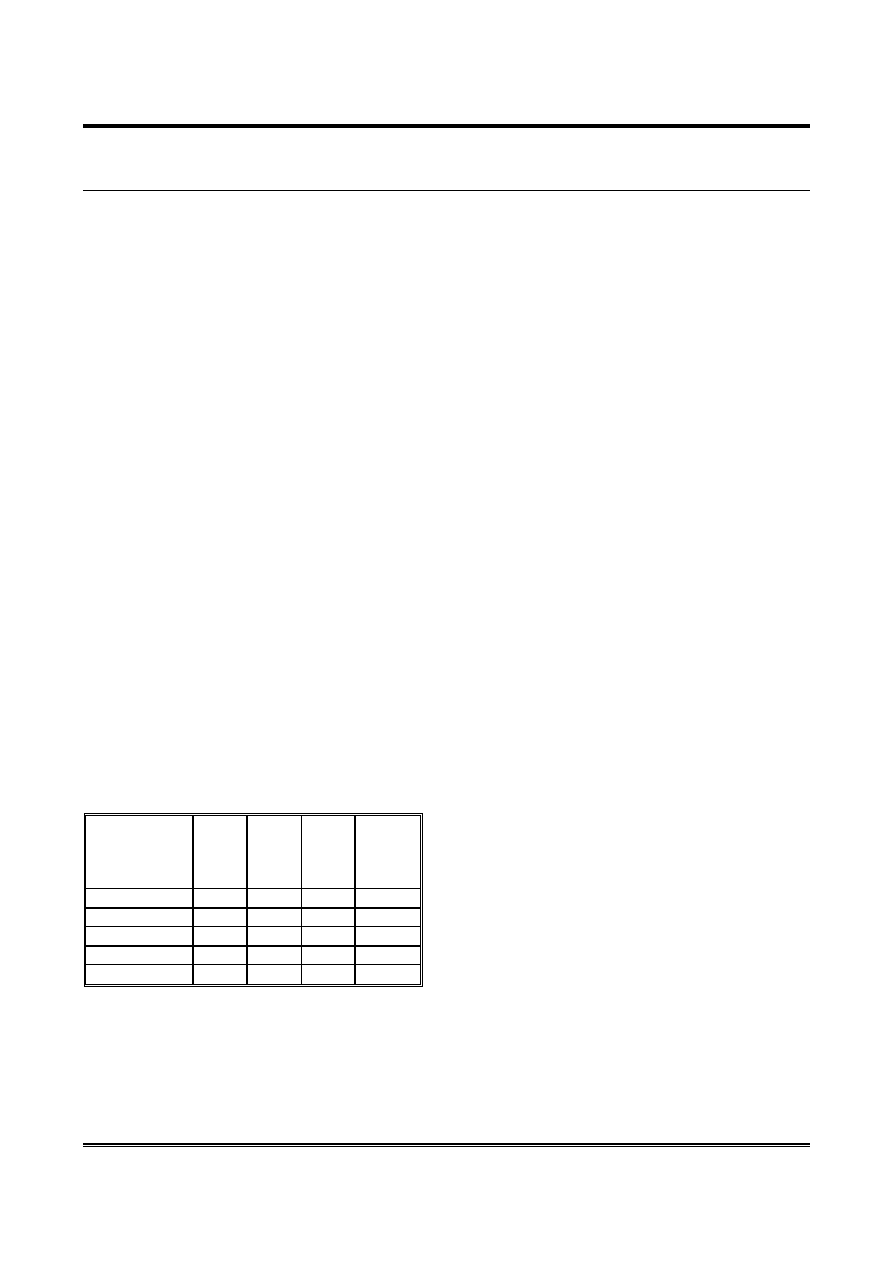
BLOCK DIAGRAM
6
5
4
3
2
1
L e v e l
S h ifte r
D e la y
S h o rt c irc u it
D e te c to r
+
-
+
-
+
-
V D 1
V D 2
V D 3
V
S S
D
O U T
C
O U T
V -
V
D D
Pin Configurations
1
2
3
4
5
6
(m a rk s id e )
PIN DESCRIPTION
Pin No.
Symbol
Pin description
1
Dout
Output of over-discharge detection, CMOS output
2
V-
Pin for charge negative input
3
Cout
Output of over-charge detection, CMOS output
4 NC
No
connection
5 VDD
Power
supply
6 Vss
Ground
TE
CH
tm
T63H0006B
TM Technology Inc. reserves the right P. 3 Publication Date: JUN. 2004
to change products or specifications without notice. Revision:B
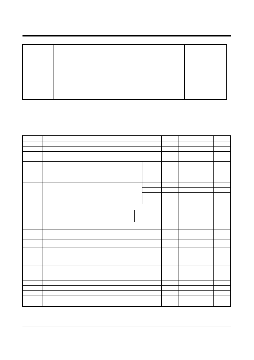
ABSOLUTE MAXIMUM RATINGS
(Vss=0V)
Symbol Item
Ratings Unit
VDD
Supply voltage
-0.3 to 12
V
V- Input
voltage
V
DD
-28 to V
DD
+0.3 V
Vcout V
DD
-28 to V
DD
+0.3 V
Vdout
Output voltage
Vss-0.3 toV
DD
+0.3 V
P
D
Power
dissipation
150
mW
Topt
Operating temperature range
-40 to85
∫C
Tstg
Storage temperature range
-55 to 125
∫C
Absolute Maximum ratings are threshold limit values that must not be exceeded ever for an instant under any conditions.
Moreover, such values for any two items must not be reached simultaneously. Operation above these absolute maximum
ratings may cause degradation or permanent damage to the device. These are stress ratings only and do not necessarily
imply functional operation below these limits.
ELECTRICAL CHARACTERISTIC
(Temp=25∫C)
Symbol Item
Conditions
MIN.
TYP.
MAX.
Unit
VDD1
Operating input voltage
Voltage defined as VDD to Vss
1.5
10
V
VDD2
Operating input voltage
Voltage defined as VDD to V-
28
V
V0inh
0V battery charge inhibition
charge voltage
Applied for 0V battery charge
inhibition function
0.8 1.0 1.2V V
-AX 4.225 4.250 4.275 V
-BX 4.325 4.350 4.375 V
-CX 4.275 4.300 4.325 V
VDET1 Over-charge
threshold
Detect rising edge of
supply voltage
-DX 4.255 4.28 4.305 V
-AX 4.025 4.050 4.075 V
-BX 4.125 4.150 4.175 V
-CX 4.075 4.100 4.125 V
VREL1
Release voltage for over-charge
detection
--
-DX 4.055 4.080 4.105 V
tVDET1
Output delay of over charge
VDD=3.6V to 4.3V
30
110
250
ms
-AX,-BX,-CX 2.400 2.500 2.600
V
VDET2 Over-discharge
threshold
Detect falling edge
of supply voltage
-DX 2.800
2.900
3.000
V
tVDET2 Output delay of over-discharge
VDD=3.6V to 2.4V
3
10
25
ms
VDET3
Excess current threshold
Detect rising edge of "V-" pin
voltage
0.13 0.15 0.17 V
tVDET3 Output delay of excess current
VDD=3.0V
4
11
26
ms
Vshort
Short protection voltage
VDD=3.0V
VDD-1.5 VDD-1.1 VDD-0.5
V
tshort
Output delay of short protection
VDD=3.0V
5
50
us
Rshort
Reset resistance for excess
current protection
VDD=3.6V, V-=1.0V
80
130
180
kOhm
Vol1
Nch ON voltage of Cout
Iol=50uA, VDD=4.4V
0.4
V
Voh1
Pch ON voltage of Cout
Iol=-50uA, VDD=3.9V
VDD-0.5
V
Vol2
Nch ON voltage of Dout
Iol=50uA, VDD=2.4V
0.4
V
Voh2
Pch ON voltage of Dout
Iol=-50uA, VDD=3.9V
VDD-0.5
V
IDD
Supply current
VDD=3.9V, V-=0V
3.0
6.0
uA
Istandby Standby
current
VDD=2.0V
0.15
0.3
uA

TE
CH
tm
T63H0006B
TM Technology Inc. reserves the right P. 4 Publication Date: JUN. 2004
to change products or specifications without notice. Revision:B
OPERATION
VD1/Over-Charge Detector
The VD1 monitors VDD pin voltage. When the
VDD voltage crosses over charge detector threshold
VDET1 from a low value to a value higher than the
VDET1, the VD1 can sense a over-charging and an
external charge control Nch-MOS-FET turns to
"OFF" with Cout pin being at "L" level.
There can be two cases to reset the VD1 making
the Cout pin level to "H" again after detecting
over-charge. Resetting the VD1 can make charging
system allowable to resumption of charging process.
The first case is in such conditions that a time when
the VDD voltage is coming down to a level lower
than "VREL1". While in the second case,
connecting a kind of loading to VDD after
disconnecting a charger from the battery pack can
make the VD1 resetting when the VDD level is in
between "VDET1" and "VREL1".
After detecting over-charge with the VDD
voltage of higher than VDET1, connecting system
load to the battery pack makes load current
allowable through parasitic diode of external charge
control FET. The Cout level would be high when the
VDD level is coming down to a level below the
VDET1 by continuous drawing of load current.
When the VDD level is going up to a higher level
than VDET1 if the VDD voltage would be back to a
level lower than the VDET1 within a time period of
the output delay time, VD1 would not output a signal
for turning off the charge control FET.
A level shifter incorporated in a buffer driver for the
Cout pin makes the "L" level of Cout pin to the V-
pin voltage and the "H" level of Cout pin is set to
VDD voltage with CMOS buffer
VD2/Over-Discharge Detector
The VD2 is monitoring a VDD pin voltage. When
the VDD voltage crosses the over-discharge detector
threshold VDET2 from a high value to a value lower
than the VDET2, the VD2 can sense an
over-discharging and the external discharge control
Nch MOSFT turns to "OFF" with the Dout pin being
at "L" level.
To reset the VD2 with the Dout pin level being
"H" again after detecting over-discharge it is
necessary to connect a charger to the battery pack for
T63H0006B. When the VDD voltage stays under
over-discharge detector threshold VDET2 charge
current can flow through parasitic diode of external
discharge control MOSFET, then after the VDD
voltage comes up to a value larger than VDET2,
Dout becomes "H" and discharging process would
be able to advance through ON state MOSFET for
discharge control.
Connecting a charger to the battery pack makes
the Dout level being "H" instantaneously when the
VDD voltage is higher than VDET2.
Besides, for T63H0006B, when a cell voltage
reaches equal or more than over-discharge released
voltage, or VDET2, over-discharge condition can be
also released.
An output delay time for the over-discharge
detection is fixed internally, tVDET2 =10ms typ. At
VDD=2.4V. When the VDD level is going down to a
lower level than VDET2 if the VDD voltage would
be back to a level higher than the VDET2 within a
time period of the output delay time, VD2 would not
output a signal for turning off the discharge control
FET.
After detection of an over-discharge by VD2,
supply current would be reduced to typ. 0.15uA at
VDD=2.0V and into standby, only the charger
detector is operating.
The output type of Dout pin is CMOS having "H"
level of VDD and "L" level of Vss.
TE
CH
tm
T63H0006B
TM Technology Inc. reserves the right P. 5 Publication Date: JUN. 2004
to change products or specifications without notice. Revision:B
VD3/Excess Current Detector, Short Circuit
Protector
Both of the excess current detector and short
circuit protector can work when both control
FETs are in "ON" state. When the V- pin
voltage is going up to a value between the short
protection voltage Vshort/VDD and excess
current threshold VDET3, the excess current
detector operates and further soaring of V- pin
voltage higher than Vshort makes the short
circuit protector enabled. This leads the external
discharge control Nch MOSFET turn off with
the Dout pin being at "L" level.
An output delay time for the excess current
detector is internally fixed, 11ms typ. At
VDD=3.0V. Aquick recovery of V- pin level
from a value between Vshort and VDET3 within
the delay time keeps the discharge control FET
staying "H" state.
When the short circuit protector is enabled,
the Dout would be low and its delay time would
be 5us typ.
The V- pin has a built-in pulled down resistor,
typ. 130kOhm with connecting to the Vss pin.
After an excess current or short circuit
protection is detected, removing a cause of
excess current or external short circuit makes an
external discharge control FET to an "ON" state
automatically with the V- pin level being down
to the Vss level through pulled down resistor
built-in internally.
If VDD voltage would be higher than VDET2
at a time when the excess current is detected the
T63H0006B does not enter a standby mode, or
otherwise in case of lower VDD voltage than
VDET2 would lead the T63H0006B into a
standby.
After detecting short circuit the T63H0006B
will not enter a standby mode.
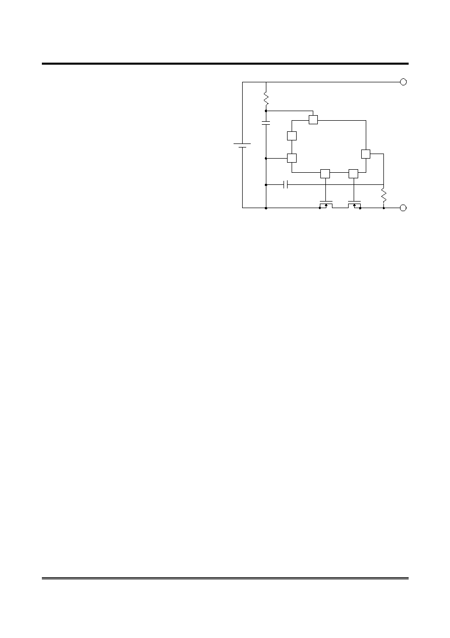
Application Circuits
6
5
4
3
2
1
-
C 1
0.1uF
C 2
0.1uF
R 2
1 k ohm
T 63H 00 06B
R 1
100 o hm
+
Application Hints
R1 and C1 will stabilize a supply voltage to
the T63H0006B. A recommended R1 value is
less than 100 Ohm. A larger value of R1 leads
higher detection voltage, makes some errors,
because of shoot through current flowed in the
T63H0006B.
R2 and C2 will stabilize a V- pin voltage. The
resetting from over-discharge with connecting a
charger possibly be disabled by larger value of
R2.
Recommended value is less than 1kOhm.
After over-charge detection even connecting
battery pack to a system probably could not
allow a system to draw load current by a larger
R2xC2 time constant in the T63H0006B.
Recommended C2 value is less than 1uF.
R1 and R2 may cause power consumption over
rating of power dissipation of the T63H0006B
and a total of "R1+R2" should be more than
1kOhm.
The time constants R1xC1 or R2xC2 must
have a relation as below:
R1xC1<=R2xC2
Because in case that R1xC1, time constant for
VDD pin, would be larger than R2xC2, time
constant for V- pin then the T63H0006B might
be into a standby mode after detecting excess
current or short circuit current.
TE
CH
tm
T63H0006B
TM Technology Inc. reserves the right P. 6 Publication Date: JUN. 2004
to change products or specifications without notice. Revision:B
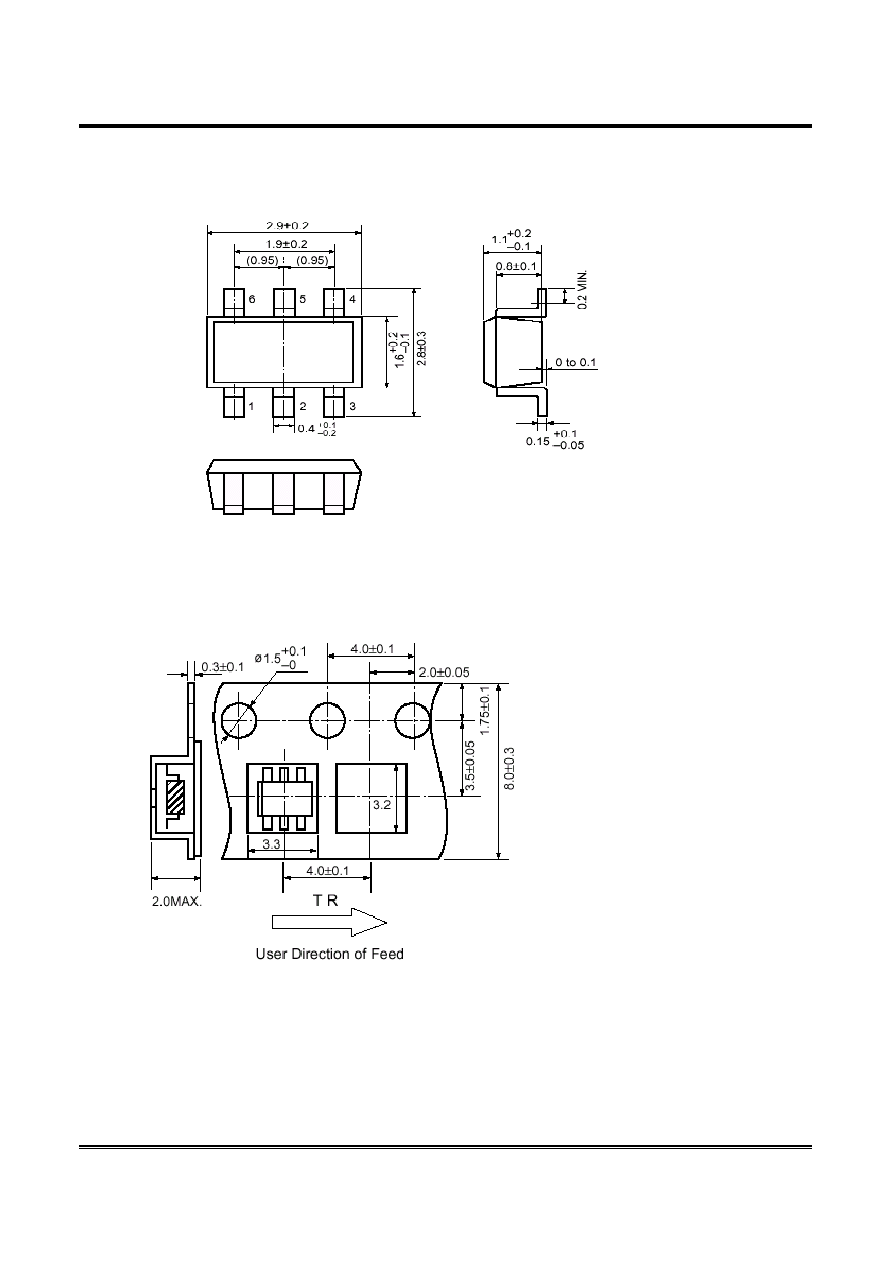
Package Dimension
(Unit: mm)
SOT-23-6
Taping Specification
(Unit: mm)
SOT-23-6