
TE
CH
tm
T66H0001A
TM Technology Inc. reserves the right P. 1 Publication Date: JUL. 2002
to change products or specifications without notice. Revision:A
T66H0001A
240 output LCD
Segment/Common
Driver IC
FEATURES
! Number of LCD drive outputs : 240
! Supply voltage for LCD drive :
( +10.0 to +42.0 V)
! Supply voltage for logic system :
( +2.5 to +5.5 V)
! Low power consumption
! Low output impedance
! Package : 269-pin TCP
(Tape Carrier Package)
DESCRIPTION
The T66H0001A is a 240-output
segment/common driver IC suitable for
driving large/medium scale dot matrix
LCD panels, and is used in personal
computers/work stations. Through the
use of SST (Super Slim TCP)
technology, it is ideal for substantially
decreasing the size of the frame section
of the LCD module. The T66H0001A is
good both as a segment driver and a
common driver, and it can create a low
power consuming, high resolution LCD
Segment mode:
1. Shift clock frequency
- 20 MHz (MAX.) : VDD = +5.0 � 0.5 V
- 15 MHz (MAX.) : VDD = +3.0 to +4.5 V
- 12 MHz (MAX.) : VDD = +2.5 to +3.0 V
2. Adopts a data bus system
3. 4-bit/8-bit parallel input modes are selectable with a mode (MD) pin
4. Automatic transfer function of an enable signal
5. Automatic counting function which, in the chip selection mode, causes the internal
clock to be stopped by automatically counting 240 bits of input data
6. Line latch circuits are reset when /DISPOFF low active
TE
CH
tm
T66H0001A
TM Technology Inc. reserves the right P. 2
Publication Date: JUL. 2002
to change products or specifications without notice. Revision:A
Common mode:
- Shift clock frequency: 4 MHz (MAX.)
- Built-in 240-bit bi-directional shift register (divisible into 120 bits x 2)
- Available in single mode (240-bit shift register) or in dual mode (120-bit shift
register x 2)
a. Y1 # Y240 Single mode
b. Y240 # Y1 Single mode
c. Y1# Y120, Y121#Y240 Dual mode
d. Y240 #Y121, Y120 # Y1 Dual mode
The above 4 shift directions are pin selectable
- Shift register circuits are reset when /DISPOFF low active
Part Number Examples
Part No.
Pkg.
Description
T66H0001A-Y TCP Pitch 0.21mm, refer to Appendix
T66H0001A COG
Refer
to
Pads List
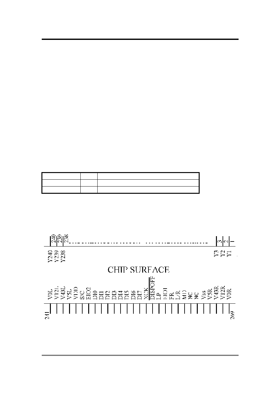
PIN CONNECTIONS
269-PIN TCP
TE
CH
tm
T66H0001A
TM Technology Inc. reserves the right P. 3
Publication Date: JUL. 2002
to change products or specifications without notice. Revision:A
PIN DESCRIPTION
PIN NO.
SYMBOL
I/O
DESCRIPTION
1 to 240
Y1-Y240
O
LCD drive output
241, 269
V
0L,
V
0R
-
Power supply for LCD drive
242, 268
V
12L
,V
12R
-
Power supply for LCD drive
243, 267
V
43L
,V
43R
-
Power supply for LCD drive
244, 266
V
5L
,V
5R
-
Power supply for LCD drive
245
VDD
-
Power supply for logic system (+2.5V to +5.5V)
246
S/C
I
Segment mode/common mode selection
247, 259
EIO
2
, EIO
1
I/O
Input/output for chip selection at segment mode/
Shift data input/output for shift register at common mode
248 to 254
DI
0
-DI
6
I
Display data input at segment mode
255 DI
7
I
Display data input at segment mode/Dual mode data input at
common mode
256
XCK
I
Clock input for taking display data at segment mode
257
/DISPOFF
I
Control input for output of non-select level
258
LP
I
Latch pules input for display data at segment mode
Shift clock input for shift register at common mode
260
FR
I
AC-converting signal input for LCD drive waveform
261
L/R
I
Input for selecting the reading direction of display data at
segment mode/Input for selecting the shift direction of shift
register at common mode
262
MD
I
Mode selection input
263, 264
NC
I
Not Connection
265 VSS -
Ground(0V)
TE
CH
tm
T66H0001A
TM Technology Inc. reserves the right P. 4
Publication Date: JUL. 2002
to change products or specifications without notice. Revision:A
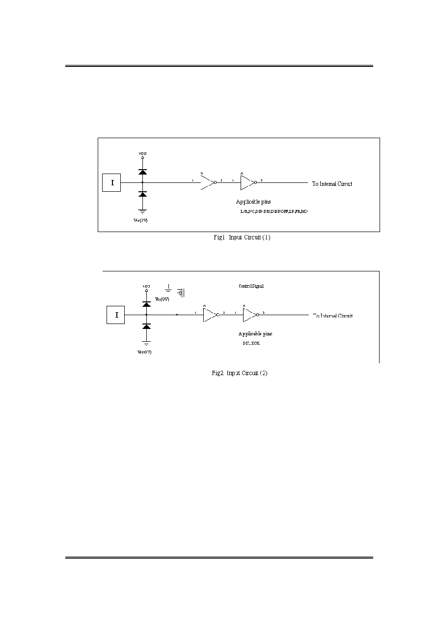
INPUT/OUTPUT CIRCUITS

TE
CH
tm
T66H0001A
TM Technology Inc. reserves the right P. 5
Publication Date: JUL. 2002
to change products or specifications without notice. Revision:A
TE
CH
tm
T66H0001A
TM Technology Inc. reserves the right P. 6
Publication Date: JUL. 2002
to change products or specifications without notice. Revision:A
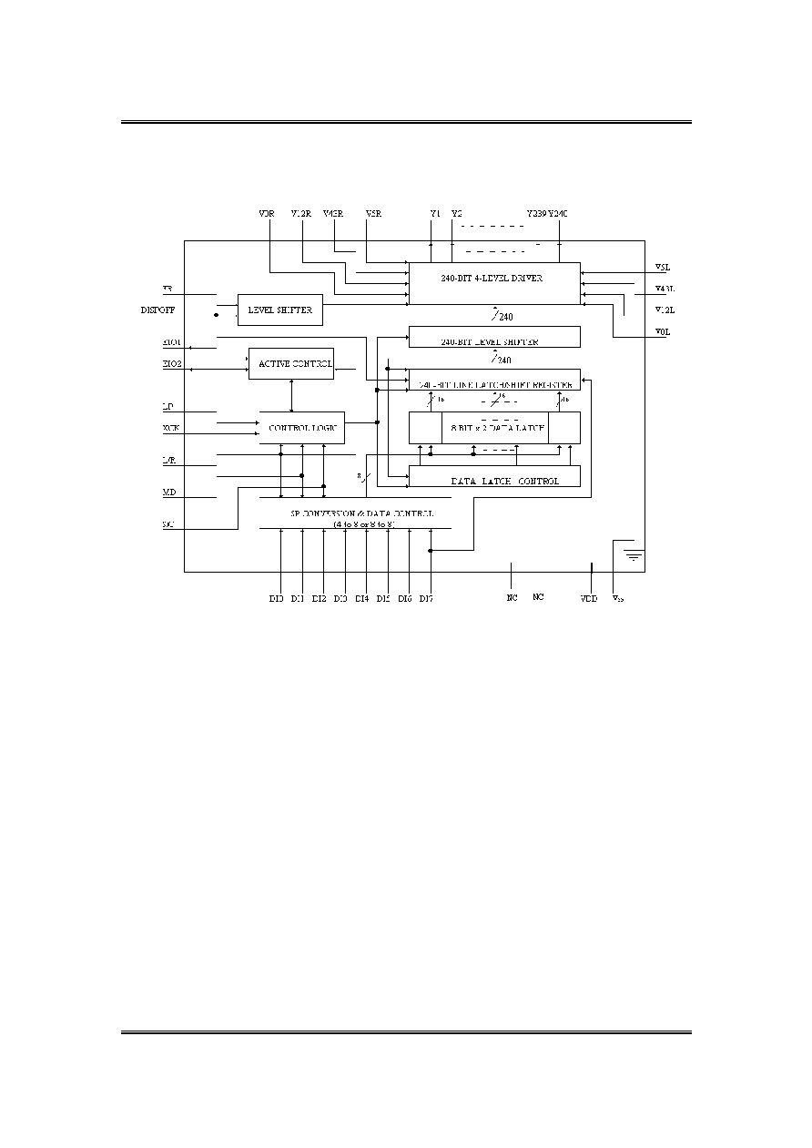
BLOCK DIAGRAM

TE
CH
tm
T66H0001A
TM Technology Inc. reserves the right P. 7
Publication Date: JUL. 2002
to change products or specifications without notice. Revision:A
FUNCTIONAL OPERATIONS OF EACH BLOCK
BLOCK FUNCTION
Active Control
In case of segment mode, controls the selection or non-selection of the chip.
Following and LP signal input, and after the chip selection signal is input, a
selection signal is generated internally until 240 bits of data have been read in.
Once data input has been completed, a selection signal for cascade connection is
output, and the chip is non-selected. In case of common mode, controls the
input/output data of bi-directional pins.
SP Conversion &
Data Control
In case of segment mode, keeps input data which are 2 clocks of XCK at 4-bit
parallel input mode in latch circuit, or keeps input data which are 1 clock of
XCK at 8-bit parallel input mode in latch circuit, after that they are put on the
internal data 8 bits at a time.
Data Latch Control
In case of segment mode, selects the state of the data latch which reads in the
data bus signals. The shift direction is controlled by the control logic. For every
16 bits of data read in, the selection signal shifts one bit based on the state of the
control circuit.
Data Latch
In case of segment mode, latches the data on the data bus. The latch state of each
LCD rive output pin is controlled by the control logic and the data latch control;
240 bits of data are read in 30 sets of 8 bits.
Line Latch/
Shift Register
In case of segment mode, all 240 bits which have been read into the data latch
are simultaneously latched at the falling edge of the LP signal, and are output to
the level shifter block. In case of common mode, shifts data from the data input
pin at the falling edge of the LP signal.
Level Shifter
The logic voltage signal is level-shifted to the LCD drive voltage level, and in
output to the driver block.
4-Level driver
Drives the LCD drive output pins from the line latch/shift register data, and
selects one of 4 levels (V
0
, V
12
, V
43
, or V
5
) based on the S/C, FR and /DISPOFF
signals.
Control Logic
Controls the operation of each block. In case of segment mode, when an LP
signal has been input, all blocks are rest and the control logic waits for the
selection signal output from the active control block. Once the selection signal
has been output, operation of the data latch and data transmission is controlled,
240 bits of data are read in, and the chip in non-selected. In case of common
mode, controls the direction of data shift.

TE
CH
tm
T66H0001A
TM Technology Inc. reserves the right P. 8
Publication Date: JUL. 2002
to change products or specifications without notice. Revision:A
FUNCTIONAL DESCRIPTION
Pin Functions
(Segment mode)
SYMBOL FUNCTION
V
DD
Logic system power supply pin, connected to +2.5 to +5.5 V.
Vss
Ground pin, connected to 0 V.
V
0L
, V
0R
V
12L
, V
12R
V
43L
, V
43R
V
5L
, V
5R
Bias power supply pins for LCD drive voltage
� Normally use the bias voltages set by a resistor divider.
� Ensure that voltages are set such that Vss V
5
< V
43
< V
12
< V
0
.
� V
iL
and V
iR
(
i= 0 , 12 , 43 , 5)
must connect to an external power supply , and supply
regular voltage which is assigned by specification for each power pin.
DI
7
, DI
0
Input pins for display data
� In 4-bit parallel input mode, input data into the 4 pins, DI
3
-DI
0
.
Connect DI
7
-DI
4
to Vss or V
DD
.
� In 8-bit parallel input mode, input data into the 8 pins, DI
7
- DI
0
.
� Refer to " RELATIONSHIP BETWEEN THE DISPLAY DATA AND LCD
DRIVE OUTPUT PINS" in Functional Operations.
XCK
Clock input pin for taking display data
� Data is read at the falling edge of the clock pulse.
LP
Latch pulse input pin for display data
� Data is latched at the falling edge of the clock pulse.
L/R
Input pin for selecting the reading direction of display data
� When set to Vss level "L", data is read sequentially from Y
240
to Y
1
.
� When set to V
DD
level "H", data is read sequentially from Y
1
to Y
240
.
� Refer to " RELATIONSHIP BETWEEN THE DISPLAY DATA AND LCD
DRIVE OUTPUT PINS" in Functional Operations.
/DISPOFF
Control input pin for output of non-select level
� The input signal is level-shifted from logic voltage level to LCD drive voltage
level, and controls the LCD drive circuit.
� When set to Vss level "L", the LCD drive output pins (Y
1
-Y
240
) are set to level V
5
.
� When set to "L" ,the contents of the line latch are reset , but the display data are
read in the data latch regardless of the condition of /DISPOFF. When the
/DISPOFF function is canceled, the driver outputs non-select level (V
12
or V
43
),
then outputs the contents of the data latch at the next falling edge of the LP. At
that time, if /DISPOFF removal time does not correspond to what is shown in AC
characteristics, it can not output the reading data correctly.
� Table of truth values is shown in "TRUTH TABLE" in Functional Operations.
FR
AC signal input pin for LCD drive waveform
� The input signal is level-shifted from logic voltage level to LCD drive voltage
level, and controls the LCD drive circuit.
� Normally it inputs a frame inversion signal.
� The LCD drive output pins' output voltage levels can be set using the line latch
output signal and the FR signal.
� Table of truth values is shown in "TRUTH TABLE" in Functional Operations.

TE
CH
tm
T66H0001A
TM Technology Inc. reserves the right P. 9
Publication Date: JUL. 2002
to change products or specifications without notice. Revision:A
SYMBOL FUNCTION
MD
Mode selection pin
� When set to Vss level "L" , 8 bit parallel input mode is set.
� When set to V
DD
level "H" , 4 bit parallel input mode is set.
� Refer to " RELATIONSHIP BETWEEN THE DISPLAY DATA AND LCD
DRIVE OUTPUT PINS" in Functional Operations.
S/C
Segment mode/common mode selection pin
� When set to V
DD
level "H" , segment mode is set.
EIO
1
, EIO
2
Input/output pins for chip selection
� When L/R input is at Vss level "L" , EIO
1
is set for output , and EIO
2
is set for
input.
� When L/R input is at V
DD
level "H" , EIO
1
is set for input , and EIO
2
is set for
output.
� During output , set to "H" while LP�/XCK is "H" and after 240 bits of data have
been read , set to "L" for one cycle (from falling edge to falling edge of XCK),
after which it returns to "H".
� During input , the chip is selected while EI is set to "L" after the LP signal is
input. The chip is non-selected after 240 bits of data have been read.
Y
1
-Y
240
LCD drive output pins
� Corresponding directly to each bit of the data latch , one level (V
0 ,
V
12 ,
V
43 ,
or V
5
)
is selected and output.
� Table of truth values is shown in "TRUTH TABLE" in Functional Operations.

TE
CH
tm
T66H0001A
TM Technology Inc. reserves the right P. 10
Publication Date: JUL. 2002
to change products or specifications without notice. Revision:A
Common mode:
SYMBOL FUNCTION
V
DD
Logic system power supply pin, connected to +2.5 to +5.5 V.
Vss
Ground pin, connected to 0 V.
V
0L
, V
0R
V
12L
, V
12R
V
43L
, V
43R
V
5L
, V
5R
Bias power supply pins for LCD drive voltage
� Normally use the bias voltages set by a resistor divider.
� Ensure that voltages are set such that Vss V
5
< V
43
< V
12
< V
0
.
� V
iL
and V
iR
(
i = 0 , 12 , 43 , 5)
must connect to an external power supply , and supply
regular voltage which is assigned by specification for each power pin.
EIO
1
Shift data input/output pin for bi-directional shift register
� Output pin when L/R is at Vss level "L" , input pin when L/R is at V
DD
level "H".
� When L/R = H, EIO
1
is used as input pin, it will be pulled down.
� When L/R = L, EIO
1
is used as output pin, it won't be pulled down.
� Refer to " RELATIONSHIP BETWEEN THE DISPLAY DATA AND LCD
DRIVE OUTPUT PINS" in Functional Operations.
EIO
2
Shift data input/output pin for bi-directional shift register
� Input pin when L/R is at Vss level "L" , output pin when L/R is at V
DD
level "H".
� When L/R = L, EIO
2
is used as input pin, it will be pulled down.
� When L/R = H, EIO
2
is used as output pin, it won't be pulled down.
� Refer to " RELATIONSHIP BETWEEN THE DISPLAY DATA AND LCD
DRIVE OUTPUT PINS" in Functional Operations.
LP
Latch pulse input pin for display data
� Data is latched at the falling edge of the clock pulse.
L/R
Input pin for selecting the shift direction of bi-directional shift register
� Data is shifted from Y
240
to Y
1
when set to Vss level "L" , and data is shifted from
Y
1
to Y
240
when set to V
DD
level "H".
� Refer to " RELATIONSHIP BETWEEN THE DISPLAY DATA AND LCD
DRIVE OUTPUT PINS" in Functional Operations.
/DISPOFF
Control input pin for output of non-select level
� The input signal is level-shifted from logic voltage level to LCD drive voltage
level, and controls the LCD drive circuit.
� When set to Vss level "L", the LCD drive output pins (Y
1
-Y
240
) are set to level V
5
.
� When set to "L", the contents of the shift register are reset to not reading data.
When the /DISPOFF function is canceled , the driver outputs non-select level (V
12
or V
43
), and the shift data is read at the next falling edge of the LP. At that time, if
DISPOFF removal time does not correspond to what is shown in AC
characteristics, the shift data is not read correctly.
� Table of truth values is shown in "TRUTH TABLE" in Functional Operations.
FR
AC signal input pin for LCD drive waveform
� The input signal is level-shifted from logic voltage level to LCD drive voltage
level, and controls the LCD drive circuit.
� Normally it inputs a frame inversion signal.
� The LCD drive output pins' output voltage levels can be set using the line latch
output signal and the FR signal.
� Table of truth values is shown in "TRUTH TABLE" in Functional Operations.
TE
CH
tm
T66H0001A
TM Technology Inc. reserves the right P. 11
Publication Date: JUL. 2002
to change products or specifications without notice. Revision:A
SYMBOL FUNCTION
MD
Mode selection pin
� When set to Vss level "L" , single operation is selected ; when set to V
DD
level "H" , dual mode operation is selected.
� Refer to " RELATIONSHIP BETWEEN THE DISPLAY DATA AND LCD
DRIVE OUTPUT PINS" in Functional Operations.
DI
7
Dual mode data input pin
� According to the data shift direction of the data shift register , data can be input
starting from the 121
st
bit.
� When the chip is used in dual mode, DI
7
will be pulled down.
� When the chip is used in single mode, DI
7
won't be pulled down.
� Refer to " RELATIONSHIP BETWEEN THE DISPLAY DATA AND LCD
DRIVE OUTPUT PINS" in Functional Operations.
S/C
Segment mode/common mode selection pin
� When set to Vss level "L, common mode is set.
DI
6
-DI
0
Not used
� Connect DI
6
-DI
0
to Vss or V
DD
, avoiding floating.
XCK
Not used
� XCK is pulled down in common mode, so connect to Vss or open.
Y
1
-Y
240
LCD drive output pins
� Corresponding directly to each bit of the data latch , one level (V
0 ,
V
12 ,
V
43 ,
or
V
5
) is selected and output.
� Table of truth values is shown in "TRUTH TABLE" in Functional Operations.

TE
CH
tm
T66H0001A
TM Technology Inc. reserves the right P. 12
Publication Date: JUL. 2002
to change products or specifications without notice. Revision:A
Functional Operations
TRUTH TABLE
(Segment Mode)
FR
Latch Data
/DISPOFF
LCD Drive Output Voltage Level (Y
1
-Y
240
)
L L H
V
43
L H H
V
5
H L H
V
12
H H H
V
0
X X L
V
5
(Common Mode)
R
Latch Data
/DISPOFF
LCD Drive Output Voltage Level (Y
1
-Y
240
)
L L H
V
43
L H H
V
0
H L H
V
12
H H H
V
5
X X L
V
5
NOTES :
�
Vss <= V
5
< V
43
< V
12
< V
0
, L: Vss (0 V), H: V
DD
(+2.5 to +5.5 V) , X : Don't care
�
"Don't care" should be fixed to "H" or "L", avoiding floating.
There are two kinds of power supply (logic level voltage and LCD drive voltage) for the LCD
driver.
Supply regular voltage which is assigned by specification for each power pin.

TE
CH
tm
T66H0001A
TM Technology Inc. reserves the right P. 13
Publication Date: JUL. 2002
to change products or specifications without notice. Revision:A
RELATIONSHIP BETWEEN THE DISPLAY DATA AND
LCD DRIVE OUTPUT PINS
(Segment Mode)
(a) 4-bit Parallel Input Mode
NUMBER OF CLOCKS
MD L/R EIO
1
EIO
2
DATA
IINPU
T
60 Clock 59 Clock 58 Clock
...
3 Clock 2 Clock 1 Clock
DI
0
Y
1
Y
5
Y
9
...
Y
229
Y
233
Y
237
DI
1
Y
2
Y
6
Y
10
...
Y
230
Y
234
Y
238
DI
2
Y
3
Y
7
Y
11
...
Y
231
Y
235
Y
239
H L
Output
Input
DI
3
Y
4
Y
8
Y
12
...
Y
232
Y
236
Y
240
DI
0
Y
240
Y
236
Y
232
...
Y
12
Y
8
Y
4
DI
1
Y
239
Y
235
Y
231
...
Y
11
Y
7
Y
3
DI
2
Y
238
Y
234
Y
230
...
Y
10
Y
6
Y
2
H H
Input
Output
DI
3
Y
237
Y
233
Y
229
...
Y
9
Y
5
Y
1

TE
CH
tm
T66H0001A
TM Technology Inc. reserves the right P. 14
Publication Date: JUL. 2002
to change products or specifications without notice. Revision:A
(b) 8 bit Parallel input Mode
NUMBER OF CLOCKS
MD L/R EIO
1
EIO
2
DATA
IINPU
T
30 Clock 29 Clock 28 Clock
...
3 Clock 2 Clock 1 Clock
DI
0
Y
1
Y
9
Y
17
...
Y
217
Y
225
Y
233
DI
1
Y
2
Y
10
Y
18
...
Y
218
Y
226
Y
234
DI
2
Y
3
Y
11
Y
19
...
Y
219
Y
227
Y
235
DI
3
Y
4
Y
12
Y
20
...
Y
220
Y
228
Y
236
DI
4
Y
5
Y
13
Y
21
...
Y
221
Y
229
Y
237
DI
5
Y
6
Y
14
Y
22
...
Y
222
Y
230
Y
238
DI
6
Y
7
Y
15
Y
23
...
Y
223
Y
231
Y
239
L L
Output
Input
DI
7
Y
8
Y
16
Y
24
...
Y
224
Y
232
Y
240
DI
0
Y
240
Y
232
Y
224
...
Y
24
Y
16
Y
8
DI
1
Y
239
Y
231
Y
223
...
Y
23
Y
15
Y
7
DI
2
Y
238
Y
230
Y
222
...
Y
22
Y
14
Y
6
DI
3
Y
237
Y
229
Y
221
...
Y
21
Y
13
Y
5
DI
4
Y
236
Y
228
Y
220
...
Y
20
Y
12
Y
4
DI
5
Y
235
Y
227
Y
219
...
Y
19
Y
11
Y
3
DI
6
Y
234
Y
226
Y
218
...
Y
18
Y
10
Y
2
L H
Input
Output
DI
7
Y
233
Y
225
Y
217
...
Y
17
Y
9
Y
1
(Common Mode)
MD
L/R
Data Transfer Direction
EIO
1
EIO
2
DI
7
L Y
240
Y
1
Output Input X
L
(Single)
H Y
1
Y
240
Input Output X
Y
240
Y
121
L
Y
120
Y
1
Output Input Input
Y
1
Y
120
H
(Dual)
H
Y
121
Y
240
Input Output Input
NOTES :
� L : Vss (0 V ) , H : V
DD
(+2.5 to +5.5 V) , X : Don
'
t care
�
"
Don
'
t care
"
should be fixed to
"
H
"
or
"
L
"
, avoiding floating.

TE
CH
tm
T66H0001A
TM Technology Inc. reserves the right P. 15
Publication Date: JUL. 2002
to change products or specifications without notice. Revision:A
CONNECTION EXAMPLES OF PLURAL SEGMENT
DRIVERS
(a) When L/R = "L"
(b) When L/R = "H"

TE
CH
tm
T66H0001A
TM Technology Inc. reserves the right P. 16
Publication Date: JUL. 2002
to change products or specifications without notice. Revision:A
CONNECTION EXAMPLES FOR PLURAL COMMON
DRIVERS
(a) Single Mode (L/R = "L")
(b) Single Mode (L/R = "H")
TE
CH
tm
T66H0001A
TM Technology Inc. reserves the right P. 17
Publication Date: JUL. 2002
to change products or specifications without notice. Revision:A
(c) Dual Mode (L/R = "L")
(d) Dual Mode (L/R = "H")

TE
CH
tm
T66H0001A
TM Technology Inc. reserves the right P. 18
Publication Date: JUL. 2002
to change products or specifications without notice. Revision:A
PRECAUTIONS
Precautions when connecting or disconnecting the power supply
This IC has a high-voltage LCD driver, so it may be permanently damaged by a high current which
may flow if voltage is supplied to the LCD drive power supply while the logic system power supply is
floating. The details are as follows.
� When connecting the power supply, connect the LCD drive power after connecting the logic system
power. Furthermore, when disconnecting the power , disconnect the logic system power after
disconnecting the LCD drive power.
� It is advisable to connect the serial resister (50 to 100 ) or fuse to the LCD drive power V
0
of the
system as a current limiter. Set up a suitable value of the resister in consideration of the display
grade. And when connecting the logic power supply, the logic condition of this IC inside is
insecurity. Therefore connect the LCD drive power supply after resetting logic condition of this IC
inside on /DISPOFF function. After that, cancel the /DISPOFF function after the LCD drive power
supply has become stable. Furthermore, when disconnecting the power , set the LCD drive output
pins to level V
5
on /DISPOFF function. Then disconnect the logic system power after disconnecting
the LCD drive power. When connecting the power supply, follow the recommended sequence shown
here.

TE
CH
tm
T66H0001A
TM Technology Inc. reserves the right P. 19
Publication Date: JUL. 2002
to change products or specifications without notice. Revision:A
ABSOLUTE MAXIMUM RATINGS
PARAMETER SYMBOL
APPLICABLE
PINS
RATING
UNIT NOTE
Supply voltage(1)
V
DD
V
DD
-0.3 to +7.0
V
V
0
V
0L,
V
0R
-0.3 to +42.0
V
V
12
V
12L,
V
12R
-0.3 to V
0
+ 0.3
V
V
43
V
43L,
V
43R
-0.3 to V
0
+ 0.3
V
Supply voltage(2)
V
5
V
5L,
V
5R
-0.3 to V
0
+ 0.3
V
Input voltage
V
I
DI
7-
DI
0
, XCK, LP, L/R,
FR, MD, S/C, EIO
1
,
EIO
2
, DISPOFF,
TEST
1,
TEST
2
-0.3 to V
DD
+ 0.3
V
1,2
Storage temperature
Tstg
-45 to +125
�C
NOTES :
1. T
A
= +25 �C
2. The maximum applicable voltage on any pin with respect to Vss (0V).
RECOMMENDED OPERATING CONDITIONS
PARAMETER
AYMBOL APPLICABLE
PINS MIN. TYP. MAX. UNIT NOTE
Supply voltage(1)
V
DD
V
DD
+2.5 +5.5 V
Supply voltage(2)
V
0
V
0L,
V
0R
+10.0 +45.0 V
1,2
Operating temperature
T
OPR
-20
+85
�C
NOTES :
1. The applicable voltage on any pin with respect to Vss (0V).
2. Ensure that voltage are set such that Vss <= V
5
< V
43
< V
12
< V
0.
TE
CH
tm
T66H0001A
TM Technology Inc. reserves the right P. 20
Publication Date: JUL. 2002
to change products or specifications without notice. Revision:A
ELECTRICAL CHARACTERISTICS
DC Characteristics
(Segment Mode) (V
SS
= V
5
= 0V, V
DD
= +2.5 to +5.5V, V
0
= +10.0 to +42.0V, T
OPR
= -20 to +85
�C)
PARAMETER SYMBOL
CONDITIONS
APPLICABLE
PINS
MIN.
TYP.
MAX.
UNIT
NOTE
Input "Low" voltage
V
IL
0.2V
DD
V
Input "High" voltage
V
IH
DI7-DI0, XCK, LP,
L/R, FR, MD, S/C,
EIO1, EIO2, /DISPOFF 0.8V
DD
V
Output "Low" voltage
V
OL
I
OL
= +0.4mA
+0.4
V
Output "High" voltage
V
OH
I
OH
= -0.4mA
EIO1, EIO2
V
DD
-0.4 V
I
LIL
V
I
= Vss
-10.0
uA
Input leakage current
I
LIH
V
I
= V
DD
DI7-DI0, XCK, LP,
L/R, FR, MD, S/C,
EIO1, EIO2, /DISPOFF
+10.0
uA
Vo=40V
1.0
1.5
Vo=30V
1.5
2.0
Output resistance
R
ON
|
�
V
ON
|
=0.5V
Vo=20V
Y
1
- Y
240
2.0
2.5
K
Standby current
I
STB
V
SS
50.0
uA
1
Supply current(1)
(Non-selection)
I
DD1
V
DD
5.0
mA
2
Supply current(2)
(Selection)
I
DD2
V
DD
5.0
mA
3
Supply current(3)
I
O
V0L,V0R
700
uA
4
NOTES :
1. V
DD
= +5.0V, V
0
= +42.0 V, V
I
= Vss.
2. V
DD
= +5.0V, V
0
= +42.0 V,f
XCK
= 20 MHz, non-load, E
I
= V
DD
. The input data is turned over by data
taking clock (4-bit parallel input mode).
3. V
DD
= +5.0V, V
0
= +42.0 V,f
XCK
= 20 MHz, non-load, E
I
= Vss. The input data is turned over by data
taking clock (4-bit parallel input mode).
4. V
DD
= +5.0V, V
0
= +42.0 V,f
XCK
= 20 MHz, f
LP
= 41.6 kHz, f
FR
= 80 Hz, non-load. The input data is
turned over by data taking clock (4-bit parallel input mode).

TE
CH
tm
T66H0001A
TM Technology Inc. reserves the right P. 21
Publication Date: JUL. 2002
to change products or specifications without notice. Revision:A
(Common Mode) (Vss = V5 = 0V, V
DD
= +2.5 to +5.5V, V
0
= +10.0 to +42.0V, T
OPR
= -20 to +85 �C)
PARAMETER SYMBOL
CONDITIONS
APPLICABLE
PINS
MIN.
TYP.
MAX.
UNIT
NOTE
Input "Low" voltage
V
IL
0.2V
DD
V
Input "High" voltage
V
IH
DI7-DI0, XCK, LP,
L/R, FR, MD, S/C,
EIO1, EIO2, /DISPOFF 0.8V
DD
V
Output "Low" voltage
V
OL
I
OL
= +0.4mA
+0.4
V
Output "High" voltage
V
OH
I
OH
= -0.4mA
EIO1, EIO2
V
DD
-0.4 V
I
LIL
V
I
= Vss
DI7-DI0, XCK, LP,
L/R, FR, MD, S/C,
EIO1, EIO2, /DISPOFF
-10.0
uA
Input leakage current
I
LIH
V
I
= V
DD
DI6-DI0, LP, L/R, FR,
MD, S/C, /DISPOFF
+10.0
uA
Input pull-down current
I
PD
V
I
= V
DD
DI7, XCK, EIO1, EIO2
100.0
uA
Vo=40V
1.0
1.5
Vo=30V
1.5
2.0
Output resistance
R
ON
|
�
V
ON
|
=0.5V
Vo=20V
Y
1
- Y
240
2.0
2.5
K
Standby current
I
STB
Vss
50.0
uA
1
Supply current(1)
I
DD
V
DD
120.0
uA
2
Supply current(2)
Io
V0L,V0R
200
uA
2
NOTES :
1.V
DD
= +5.0V, V
0
= +42.0 V, V
I
= Vss.
2.V
DD
= +5.0V, V
0
= +42.0 V,f
XCK
= 20 MHz, f
LP
= 41.6 kHz, f
FR
= 80 Hz, 1/480 duty operation,
no-load.
TE
CH
tm
T66H0001A
TM Technology Inc. reserves the right P. 22
Publication Date: JUL. 2002
to change products or specifications without notice. Revision:A
AC Characteristics
(Segment Mode 1) (Vss = V
5
= 0V, V
DD
= +5.0 �0.5V, V
0
= +10.0 to +42.0V, T
OPR
= -20 to +85 �C)
PARAMETER SYMBOL
CONDITIONS
MIN.
TYP.
MAX.
UNIT
NOTE
Shift clock period
twck
t
R
,t
F
10 ns
50 ns 1
Shift clock "H" pulse width
twckh
15
ns
Shift clock "L" pulse width
twckl
15
ns
Data setup time
t
DS
10
ns
Data hold time
t
DH
12
ns
Latch pulse "H" pulse width
t
wLPH
15
ns
Shift clock rise to latch pulse rise time
t
LD
0
ns
Shift clock fall to latch pulse fall time
t
SL
30
ns
Latch pulse rise to shift clock rise time
t
LS
25
ns
Latch pulse fall to shift clock fall time
t
LH
25
ns
Enable setup time
ts
10
ns
Input signal rise time
t
R
50
ns
2
Input signal fall time
t
F
50
ns
2
/DISPOFF removal time
t
SD
100
ns
/DISPOFF "L" pulse width
t
WDL
1.2
us
Output delay time (1)
t
D
C
L=
15 pF
30
ns
Output delay time (2)
t
PD1,
t
PD2
C
L=
15 pF
1.2
us
Output delay time (3)
t
PD3
C
L=
15 pF
1.2
us
NOTES :
1. Takes the cascade connection into consideration
2. (twck - twck
H
� twck
L
)/2 is maximum in the case of high speed operation.
(Segment Mode 2) (Vss = V
5
= 0V, V
DD
= +3.0 to +4.5V, V
0
= +10.0 to +42.0V, T
OPR
= -20 to +85 �C)
PARAMETER SYMBOL
CONDITIONS
MIN.
TYP.
MAX.
UNIT
NOTE
Shift clock period
twck
t
R
,t
F
10 ns
66 ns 1
Shift clock "H" pulse width
twckh
23
ns
Shift clock "L" pulse width
twckl
23
ns
Data setup time
t
DS
15
ns
Data hold time
t
DH
23
ns
Latch pulse "H" pulse width
t
wLPH
30
ns
Shift clock rise to latch pulse rise time
t
LD
0
ns
Shift clock fall to latch pulse fall time
t
SL
50
ns
Latch pulse rise to shift clock rise time
t
LS
30
ns
Latch pulse fall to shift clock fall time
t
LH
30
ns
Enable setup time
ts
15
ns
Input signal rise time
t
R
50
ns
2
Input signal fall time
t
F
50
ns
2
/DISPOFF removal time
t
SD
100
ns
/DISPOFF "L" pulse width
t
WDL
1.2
us
Output delay time (1)
t
D
C
L=
15 pF
41
ns
Output delay time (2)
t
PD1,
t
PD2
C
L=
15 pF
1.2
us
Output delay time (3)
t
PD3
C
L=
15 pF
1.2
us
NOTES :
1. Takes the cascade connection into consideration
2. (twck - twck
H
� twck
L
)/2 is maximum in the case of high speed operation.
TE
CH
tm
T66H0001A
TM Technology Inc. reserves the right P. 23
Publication Date: JUL. 2002
to change products or specifications without notice. Revision:A
(Segment Mode 3) (Vss = V
5
= 0V, V
DD
= +2.5 to +3.0V, V
0
= +10.0 to +42.0V, T
OPR
= -20 to +85 �C)
PARAMETER SYMBOL
CONDITIONS
MIN.
TYP.
MAX.
UNIT
NOTE
Shift clock period
t
wck
t
R
,t
F
10 ns
82 ns 1
Shift clock "H" pulse width
t
wckh
28
ns
Shift clock "L" pulse width
t
wckl
28
ns
Data setup time
t
DS
20
ns
Data hold time
t
DH
23
ns
Latch pulse "H" pulse width
t
wLPH
30
ns
Shift clock rise to latch pulse rise time
t
LD
0
ns
Shift clock fall to latch pulse fall time
t
SL
65
ns
Latch pulse rise to shift clock rise time
t
LS
30
ns
Latch pulse fall to shift clock fall time
t
LH
30
ns
Enable setup time
ts
15
ns
Input signal rise time
t
R
50
ns
2
Input signal fall time
t
F
50
ns
2
/DISPOFF removal time
t
SD
100
ns
/DISPOFF "L" pulse width
t
WDL
1.2
us
Output delay time (1)
t
D
C
L=
15 pF
57
ns
Output delay time (2)
t
PD1,
t
PD2
C
L=
15 pF
1.2
us
Output delay time (3)
t
PD3
C
L=
15 pF
1.2
us
NOTES :
1. Takes the cascade connection into consideration
2. (twck - twck
H
� twck
L
)/2 is maximum in the case of high speed operation.

TE
CH
tm
T66H0001A
TM Technology Inc. reserves the right P. 24
Publication Date: JUL. 2002
to change products or specifications without notice. Revision:A
Timing Chart of Segment Mode

TE
CH
tm
T66H0001A
TM Technology Inc. reserves the right P. 25
Publication Date: JUL. 2002
to change products or specifications without notice. Revision:A
(Common Mode ) (Vss = V
5
= 0V, V
DD
= +2.5 to +5.5V, V
0
= +10.0 to +42.0V, T
OPR
= -20 to +85 �C)
PARAMETER SYMBOL
CONDITIONS
MIN.
TYP.
MAX.
UNIT
Shift clock period
twck
t
R
,t
F
10 ns
250
ns
V
DD
= +5.0�0.5V
15
ns
Shift clock "H" pulse width
twck
H
V
DD
= +2.5 to+4.5V
30
ns
Data setup time
t
SU
30
ns
Data hold time
t
H
50
ns
Input signal rise time
t
R
50
ns
Input signal fall time
t
F
50
ns
/DISPOFF removal time
t
SD
100
ns
/DISPOFF "L" pulse width
t
WDL
1.2
us
Output delay time (1)
t
DL
C
L
= 15 pF
200
ns
Output delay time (2)
t
PD1
,t
PD2
C
L
= 15 pF
1.2
us
Output delay time (3)
t
PD3
C
L
= 15 pF
1.2
us
TE
CH
tm
T66H0001A
TM Technology Inc. reserves the right P. 26
Publication Date: JUL. 2002
to change products or specifications without notice. Revision:A
Timing Chart of Common Mode

TE
CH
tm
T66H0001A
TM Technology Inc. reserves the right P. 27
Publication Date: JUL. 2002
to change products or specifications without notice. Revision:A
Timing Chart Of 4-Device Cascade Connection Of Segment Drivers

TE
CH
tm
T66H0001A
TM Technology Inc. reserves the right P. 28
Publication Date: JUL. 2002
to change products or specifications without notice. Revision:A
SYSTEM CONFIGURATION EXAMPLE

TE
CH
tm
T66H0001A
TM Technology Inc. reserves the right P. 29
Publication Date: JUL. 2002
to change products or specifications without notice. Revision:A
Pads List
"D" means dummy pads which are floating inside the chip.
PAD SIZE : OUTPAD = 55x72(Pad 1 to Pad 240)
INPAD = 70x72(Pad 241 to Pad 295) DUMMY = 70x80
OPEN WINDOW : OUTPAD = 29x46 INPAD = 44x46 DUMMY =
44x54
BUMP SIZE : OUTPAD = 43x60 INPAD = 54x56 DUMMY = 54x64
BUMP HEIGHT = 18
DIE SIZE = 14900 X 1070 (WITHOUT SCRIBE LINE)
SCRIBE LINE = 80
UNIT = um
P A D 1
P A D 2 4 0
P A D 2 4 1
P A D 2 9 5
T 6 6 H 0 0 0 1 A
D
D
D
D
D
D
D
D
D
D
D
D

TE
CH
tm
T66H0001A
TM Technology Inc. reserves the right P. 30
Publication Date: JUL. 2002
to change products or specifications without notice. Revision:A
Pad No. Pin Name
X
Y
Pad No. Pin Name
X
Y
1
Y1
7185.95 418.4
38
Y38
4965.95 418.4
2
Y2
7125.95 418.4
39
Y39
4905.95 418.4
3
Y3
7065.95 418.4
40
Y40
4845.95 418.4
4
Y4
7005.95 418.4
41
Y41
4785.95 418.4
5
Y5
6945.95 418.4
42
Y42
4725.95 418.4
6
Y6
6885.95 418.4
43
Y43
4665.95 418.4
7
Y7
6825.95 418.4
44
Y44
4605.95 418.4
8
Y8
6765.95 418.4
45
Y45
4545.95 418.4
9
Y9
6705.95 418.4
46
Y46
4485.95 418.4
10
Y10
6645.95 418.4
47
Y47
4425.95 418.4
11
Y11
6585.95 418.4
48
Y48
4365.95 418.4
12
Y12
6525.95 418.4
49
Y49
4305.95 418.4
13
Y13
6465.95 418.4
50
Y50
4245.95 418.4
14
Y14
6405.95 418.4
51
Y51
4185.95 418.4
15
Y15
6345.95 418.4
52
Y52
4125.95 418.4
16
Y16
6285.95 418.4
53
Y53
4065.95 418.4
17
Y17
6225.95 418.4
54
Y54
4005.95 418.4
18
Y18
6165.95 418.4
55
Y55
3945.95 418.4
19
Y19
6105.95 418.4
56
Y56
3885.95 418.4
20
Y20
6045.95 418.4
57
Y57
3825.95 418.4
21
Y21
5985.95 418.4
58
Y58
3765.95 418.4
22
Y22
5925.95 418.4
59
Y59
3705.95 418.4
23
Y23
5865.95 418.4
60
Y60
3645.95 418.4
24
Y24
5805.95 418.4
61
Y61
3585.95 418.4
25
Y25
5745.95 418.4
62
Y62
3525.95 418.4
26
Y26
5685.95 418.4
63
Y63
3465.95 418.4
27
Y27
5625.95 418.4
64
Y64
3405.95 418.4
28
Y28
5565.95 418.4
65
Y65
3345.95 418.4
29
Y29
5505.95 418.4
66
Y66
3285.95 418.4
30
Y30
5445.95 418.4
67
Y67
3225.95 418.4
31
Y31
5385.95 418.4
68
Y68
3165.95 418.4
32
Y32
5325.95 418.4
69
Y69
3105.95 418.4
33
Y33
5265.95 418.4
70
Y70
3045.95 418.4
34
Y34
5205.95 418.4
71
Y71
2985.95 418.4
35
Y35
5145.95 418.4
72
Y72
2925.95 418.4
36
Y36
5085.95 418.4
73
Y73
2865.95 418.4
37
Y37
5025.95 418.4
74
Y74
2805.95 418.4

TE
CH
tm
T66H0001A
TM Technology Inc. reserves the right P. 31
Publication Date: JUL. 2002
to change products or specifications without notice. Revision:A
Pad No. Pin Name
X
Y
Pad No. Pin Name
X
Y
75
Y75
2745.95 418.4
112
Y112
525.95 418.4
76
Y76
2685.95 418.4
113
Y113
465.95 418.4
77
Y77
2625.95 418.4
114
Y114
405.95 418.4
78
Y78
2565.95 418.4
115
Y115
345.95 418.4
79
Y79
2505.95 418.4
116
Y116
285.95 418.4
80
Y80
2445.95 418.4
117
Y117
225.95 418.4
81
Y81
2385.95 418.4
118
Y118
165.95 418.4
82
Y82
2325.95 418.4
119
Y119
105.95 418.4
83
Y83
2265.95 418.4
120
Y120
45.95 418.4
84
Y84
2205.95 418.4
121
Y121
-46.25 418.4
85
Y85
2145.95 418.4
122
Y122
-106.25 418.4
86
Y86
2085.95 418.4
123
Y123
-166.25 418.4
87
Y87
2025.95 418.4
124
Y124
-226.25 418.4
88
Y88
1965.95 418.4
125
Y125
-286.25 418.4
89
Y89
1905.95 418.4
126
Y126
-346.25 418.4
90
Y90
1845.95 418.4
127
Y127
-406.25 418.4
91
Y91
1785.95 418.4
128
Y128
-466.25 418.4
92
Y92
1725.95 418.4
129
Y129
-526.25 418.4
93
Y93
1665.95 418.4
130
Y130
-586.25 418.4
94
Y94
1605.95 418.4
131
Y131
-646.25 418.4
95
Y95
1545.95 418.4
132
Y132
-706.25 418.4
96
Y96
1485.95 418.4
133
Y133
-766.25 418.4
97
Y97
1425.95 418.4
134
Y134
-826.25 418.4
98
Y98
1365.95 418.4
135
Y135
-886.25 418.4
99
Y99
1305.95 418.4
136
Y136
-946.25 418.4
100
Y100
1245.95 418.4
137
Y137
-1006.25 418.4
101
Y101
1185.95 418.4
138
Y138
-1066.25 418.4
102
Y102
1125.95 418.4
139
Y139
-1126.25 418.4
103
Y103
1065.95 418.4
140
Y140
-1186.25 418.4
104
Y104
1005.95 418.4
141
Y141
-1246.25 418.4
105
Y105
945.95 418.4
142
Y142
-1306.25 418.4
106
Y106
885.95 418.4
143
Y143
-1366.25 418.4
107
Y107
825.95 418.4
144
Y144
-1426.25 418.4
108
Y108
765.95 418.4
145
Y145
-1486.25 418.4
109
Y109
705.95 418.4
146
Y146
-1546.25 418.4
110
Y110
645.95 418.4
147
Y147
-1606.25 418.4
111
Y111
585.95 418.4
148
Y148
-1666.25 418.4

TE
CH
tm
T66H0001A
TM Technology Inc. reserves the right P. 32
Publication Date: JUL. 2002
to change products or specifications without notice. Revision:A
Pad No. Pin Name
X
Y
Pad No. Pin Name
X
Y
149
Y149
-1726.25 418.4 186
Y186
-3946.25 418.4
150
Y150
-1786.25 418.4 187
Y187
-4006.25 418.4
151
Y151
-1846.25 418.4 188
Y188
-4066.25 418.4
152
Y152
-1906.25 418.4 189
Y189
-4126.25 418.4
153
Y153
-1966.25 418.4 190
Y190
-4186.25 418.4
154
Y154
-2026.25 418.4 191
Y191
-4246.25 418.4
155
Y155
-2086.25 418.4 192
Y192
-4306.25 418.4
156
Y156
-2146.25 418.4 193
Y193
-4366.25 418.4
157
Y157
-2206.25 418.4 194
Y194
-4426.25 418.4
158
Y158
-2266.25 418.4 195
Y195
-4486.25 418.4
159
Y159
-2326.25 418.4 196
Y196
-4546.25 418.4
160
Y160
-2386.25 418.4 197
Y197
-4606.25 418.4
161
Y161
-2446.25 418.4 198
Y198
-4666.25 418.4
162
Y162
-2506.25 418.4 199
Y199
-4726.25 418.4
163
Y163
-2566.25 418.4 200
Y200
-4786.25 418.4
164
Y164
-2626.25 418.4 201
Y201
-4846.25 418.4
165
Y165
-2686.25 418.4 202
Y202
-4906.25 418.4
166
Y166
-2746.25 418.4 203
Y203
-4966.25 418.4
167
Y167
-2806.25 418.4 204
Y204
-5026.25 418.4
168
Y168
-2866.25 418.4 205
Y205
-5086.25 418.4
169
Y169
-2926.25 418.4 206
Y206
-5146.25 418.4
170
Y170
-2986.25 418.4 207
Y207
-5206.25 418.4
171
Y171
-3046.25 418.4 208
Y208
-5266.25 418.4
172
Y172
-3106.25 418.4 209
Y209
-5326.25 418.4
173
Y173
-3166.25 418.4 210
Y210
-5386.25 418.4
174
Y174
-3226.25 418.4 211
Y211
-5446.25 418.4
175
Y175
-3286.25 418.4 212
Y212
-5506.25 418.4
176
Y176
-3346.25 418.4 213
Y213
-5566.25 418.4
177
Y177
-3406.25 418.4 214
Y214
-5626.25 418.4
178
Y178
-3466.25 418.4 215
Y215
-5686.25 418.4
179
Y179
-3526.25 418.4 216
Y216
-5746.25 418.4
180
Y180
-3586.25 418.4 217
Y217
-5806.25 418.4
181
Y181
-3646.25 418.4 218
Y218
-5866.25 418.4
182
Y182
-3706.25 418.4 219
Y219
-5926.25 418.4
183
Y183
-3766.25 418.4 220
Y220
-5986.25 418.4
184
Y184
-3826.25 418.4 221
Y221
-6046.25 418.4
185
Y185
-3886.25 418.4 222
Y222
-6106.25 418.4

TE
CH
tm
T66H0001A
TM Technology Inc. reserves the right P. 33
Publication Date: JUL. 2002
to change products or specifications without notice. Revision:A
Pad No. Pin Name
X
Y
Pad No. Pin Name
X
Y
223
Y223
-6166.25 418.4 260
DI1
-3398.05 -454
224
Y224
-6226.25 418.4 261
DI2
-3292.95 -454
225
Y225
-6286.25 418.4 262
DI2
-3189.45 -454
226
Y226
-6346.25 418.4 263
DI3
-3058.05 -454
227
Y227
-6406.25 418.4 264
DI3
-2954.55 -454
228
Y228
-6466.25 418.4 265
DI4
2596.4 -454
229
Y229
-6526.25 418.4 266
DI4
2699.9 -454
230
Y230
-6586.25 418.4 267
DI5
2805 -454
231
Y231
-6646.25 418.4 268
DI5
2908.5 -454
232
Y232
-6706.25 418.4 269
DI6
3039.9 -454
233
Y233
-6766.25 418.4 270
DI6
3143.4 -454
234
Y234
-6826.25 418.4 271
DI7
3248.5 -454
235
Y235
-6526.25 418.4 272
DI7
3352 -454
236
Y236
-6586.25 418.4 273
XCK
3483.4 -454
237
Y237
-6646.25 418.4 274
XCK
3586.9 -454
238
Y238
-6706.25 418.4 275
DISPOFF
3692 -454
239
Y239
-6766.25 418.4 276
DISPOFF
3795.5 -454
240
Y240
-6826.25 418.4 277
LP
3926.9 -454
241
V0L
-7154.4 -454
278
LP
4030.4 -454
242
V0L
-7069.4 -454
279
EIO1
4135.5 -454
243
V12L
-6934 -454
280
EIO1
4239 -454
244
V12L
-6849 -454
281
FR
4370.4 -454
245
V43L
-6713.6 -454
282
FR
4473.9 -454
246
V43L
-6628.6 -454
283
LR24
4616.9 -454
247
V5L
-6493.2 -454
284
LR24
4720.4 -454
248
V5L
-6408.2 -454
285
MD
4880.85 -454
249
GND
-5043.05 -454 286
GND
5069.45 -454
250
GND
-4958.05 -454 287
GND
5154.45 -454
251
VDD
-4454.3 -454
288
V5R
6408.2 -454
252
VDD
-4369.3 -454
289
V5R
6493.2 -454
253
SC
-4179.95 -454 290
V43R 6628.6
-454
254
SC
-4076.45 -454 291
V43R
6713.6 -454
255
EIO2
-3945.05 -454 292
V12R
6849 -454
256
EIO2
-3841.55 -454 293
V12R
6934 -454
257
DI0
-3736.45 -454 294
V0R
7069.4 -454
258
DI0
-3632.95 -454 295
V0R
7154.4 -454
259
DI1
-3501.55
-454
TE
CH
tm
T66H0001A
TM Technology Inc. reserves the right P. 34
Publication Date: JUL. 2002
to change products or specifications without notice. Revision:A
Pad No.
Pin
Name
X Y
Dummy
RT
7370
339.75
7291.35
449.85
LT
-7291.35
449.85
-7370
339.75
LB
-7370
-360.4
-7274.5
-449.85
Middle
-2355.85
-449.85
-2137
-449.85
-1674.8
-449.85
2356.45
-449.85
RB
7274.5 -449.85
7370
-360.4
Appendix:
