
TE
CH
tm
T81L0003B
TM Technology Inc. reserves the right P. 1 Publication Date: NOV. 2005
to change products or specifications without notice. Revision:A
8-bit MCU
1. Features
! Compatible with MCS-51
! Embedded 8K Bytes OTP ROM
! 256 x 8-bit Internal RAM
! 13 Programmable I/O Lines for 18-pin
Package
! 2 16-bit Timer/Counter & 1 16-bit Timer
! 2 External Interrupt Input
! Programmable Serial UART Interface
! Low Power Idle & Power-down Modes
! Watch-dog Timer
! On-chip Crystal & RC Oscillator (Selected
by Bonding Option)
! Internal Power-on Reset and External Reset
Supported
! SOP18/DIP18 Package
! 3.3V Operating Voltage
2. General Description
The T81L0003B is 8-bit microcontroller
designed and developed with low power and high
speed CMOS technology. It contains a 8K bytes
OTP ROM, a 256 � 8 RAM, 13 I/O lines, a
watchdog timer, two 16-bit counter/timers, a
seven source, two-priority level nested interrupt
structure, a full duplex UART, and an on-chip
oscillator and clock circuits.
In addition, the T81L0003B has two selectable
modes of power reduction-idle mode and
power-down mode. The idle mode freezes the
CPU while allowing the RAM, timers, serial port,
and interrupt system to continue functioning. The
power-down mode saves the RAM contents but
freezes the oscillator, causing all other chip
functions to be inoperative.

TE
CH
tm
T81L0003B
TM Technology Inc. reserves the right P. 2 Publication Date: NOV. 2005
to change products or specifications without notice. Revision:A
3. Block Diagram
Port 1 Drivers
RAM Addr.
Register
RAM
Port 1
Latch
OTP
ROM
B
Register
ACC
Stack
Pointer
TMP2
TMP1
ALU
PSW
Interrupt, Serial port,
and Timer Block
Timing &
Control
Instruction
Register
Port 3
Latch
Port 3 Drivers
Program Address
Register
Buffer
PC
Incrementer
Program
Counter
DPTR
P1.0 -P1.7
P3.0 -P3.4
RST
OSC
WDT
XTAL2
XTAL1
TE
CH
tm
T81L0003B
TM Technology Inc. reserves the right P. 3 Publication Date: NOV. 2005
to change products or specifications without notice. Revision:A
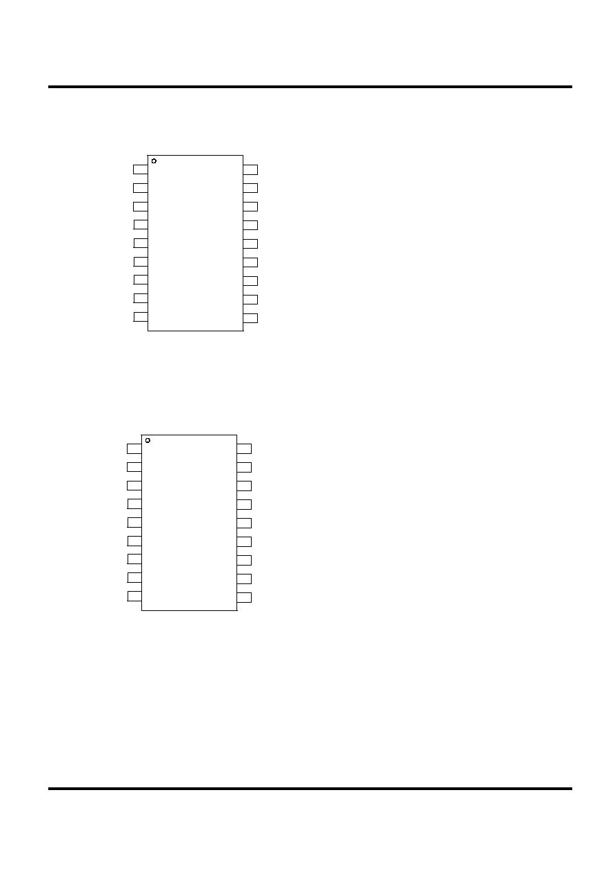
4. Pin Configuration
DIP-18/SOP-18 For Crystal Oscillator
T81L0003B-BK/ T81L0003B-BD
DIP-18/SOP-18 For RC Oscillator
T81L0003B-AK/ T81L0003B-AD
(RXD) P3.0
RST/VPP
(TXD) P3.1
1
2
3
VCC
P1.7
P1.6
P1.5
P1.4
P1.3
16
18
17
P1.2
13
15
14
P1.1
P1.0
XOUT
XIN
4
5
6
(INT0) P3.2
(INT1) P3.3
7
8
9
(T0) P3.4
GND
10
11
12
(RXD) P3.0
RST/VPP
(TXD) P3.1
1
2
3
VCC
P1.7
P1.6
P1.5
P1.4
P1.3
16
18
17
P1.2
13
15
14
P1.1
P1.0
OSCR
STOP
4
5
6
(INT0) P3.2
(INT1) P3.3
7
8
9
(T0) P3.4
GND
10
11
12

TE
CH
tm
T81L0003B
TM Technology Inc. reserves the right P. 4 Publication Date: NOV. 2005
to change products or specifications without notice. Revision:A
5. Pin Description
Number
(20-Pin)
Name Type
Description
1 RST/VPP
I
Reset signal input or programming supply voltage input.
2 P3.0/(RXD)
I/O
General-purpose I/O pin (Default) or Serial input port.
3 P3.1/(TXD)
I/O
General-purpose I/O pin (Default) or Serial output port.
4(BK,BD) XOUT O
Crystal oscillator output terminal.
4(AK,AD) OSCR I
RC oscillator external resister connect pin.
5(BK,BD) XIN I
Crystal oscillator input terminal.
5(AK,AD) STOP O
Stop RC oscillator network.
6 P3.2/(INT0)
I/O
General-purpose I/O pin (Default) or External interrupt source 0.
7 P3.3/(INT1)
I/O
General-purpose I/O pin (Default) or External interrupt source 1.
8 P3.4/(T0)
I/O
General-purpose I/O pin (Default) or Timer 0 external input pin.
9 GND
Ground
10 P1.0
I/O
General-purpose I/O pin
11 P1.1
I/O
General-purpose I/O pin
12 P1.2
I/O
General-purpose I/O pin
13 P1.3
I/O
General-purpose I/O pin
14 P1.4
I/O
General-purpose I/O pin
15 P1.5
I/O
General-purpose I/O pin
16 P1.6
I/O
General-purpose I/O pin
17 P1.7
I/O
General-purpose I/O pin
18 VCC
3.3V power supply.

TE
CH
tm
T81L0003B
TM Technology Inc. reserves the right P. 5 Publication Date: NOV. 2005
to change products or specifications without notice. Revision:A
6. Temperature Limit Ratings
Parameter Rating
Units
Operating temperature Range
-40 to +85
�C
Storage Temperature Range
-55 to +125
�C
7. Electrical Characteristics
D.C Characteristics
Symbol Parameter
Conditions Min
Typ
Max
Units
V
CC
Operating
Voltage
25�C
3.0
3.3
3.6 V
I
CC
Operating Current
No load, Vcc=3.3V
-
5
-
mA
I
PD
Power down mode current
No load
-
1
-
uA
V
IH
Hi-Level input voltage
V
out
>=V
VOH(MIN.)
V
out
<=V
VOL(MIN.)
2.1 - - V
V
IL
Low-Level input voltage
V
out
>=V
VOH(MIN.)
V
out
<=V
VOL(MIN.)
- - 0.6
V
I
OH
=-7uA 2.9
I
OH
=-45uA 2.4
V
OH
Hi-Level Output voltage
V
CC
=MIN.
V
I
=V
IH
or
V
IL
I
OH
=-70uA 1.9
- - V
I
OL
=12mA 0.2
I
OL
=25mA 0.4
V
OL
1
(P1.0 only)
Low-Level Output voltage
V
CC
=MIN.
V
I
=V
IH
or
V
IL
I
OL
=40mA
- -
0.6
V
I
OL
=4mA 0.2
I
OL
=12mA 0.4
V
OL
2
(Else Pins)
Low-Level Output voltage
V
CC
=MIN.
V
I
=V
IH
or
V
IL
I
OL
=20mA
0.6
V
A.C Characteristics
Symbol Parameter Conditions
Min
Typ
Max
Units
F
SYS1
System Clock 1
(Crystal OSC)
V
CC
=3.3V - 12 24 MHz
F
SYS2
System Clock 2
(RC OSC)
V
CC
=3.3V - 12 - MHz
t
RES
External Reset High Pulse Width
-
10
-
system cycle
Power ON Start up Time
-
20
-
ms

TE
CH
tm
T81L0003B
TM Technology Inc. reserves the right P. 6 Publication Date: NOV. 2005
to change products or specifications without notice. Revision:A
8. Function Description
8.1. Special Function Register
F8H
F0H
B
E8H
E0H
ACC
D8H
D0H
PSW
C8H T2CON
T2MOD
TL2 TH2
C0H
B8H
IP
B0H
P3
A8H
IE
98H
SCON
SBUF
90H
P1
88H TCON
TMOD TL0 TL1 TH0 TH1
Accumulator : ACC
ACC is the Accumulator register. The mnemonics for Accumulator-Specific instructions, however, refer to the
Accumulator simply as A.
B Register : B
The B register is used during multiply and divide operations. For other instructions it can be treated as another scratch
pad register.
Program Status Word : PSW
The PSW register contains program status information as detailed in
CY AC F0 RS1 RS0 OV -- P
BIT SYMBOL FUNCTION
PSW.7 CY Carry flag.
PSW.6 AC Auxiliary Carry flag. (For BCD operations.)
PSW.5 F0 Flag 0. (Available to the user for general purposes.)
PSW.4 RS1 Register bank select control bit 1.
Set/cleared by software to determine working register bank. (See Note.)
PSW.3 RS0 Register bank select control bit 0.
Set/cleared by software to determine working register bank. (See Note.)
PSW.2 OV Overflow flag.
PSW.1 -- User-definable flag.
PSW.0 P Parity flag.
Set/cleared by hardware each instruction cycle to indicate an odd/even number of "one" bits in the
Accumulator, i.e., even parity.
NOTE: The contents of (RS1, RS0) enable the working register banks as follows:
(0,0)-- Bank 0 (00H�07H)
(0,1)-- Bank 1 (08H�0fH)
(1,0)-- Bank 2 (10H�17H)
(1,1)-- Bank 3 (18H�17H)

TE
CH
tm
T81L0003B
TM Technology Inc. reserves the right P. 7 Publication Date: NOV. 2005
to change products or specifications without notice. Revision:A
Stack Pointer : SP
The Stack Pointer register is 8 bits wide. It is incremented before data is stored during PUSH and CALL executions.
While the stack may reside anywhere in on-chip RAM, the Stack Pointer is initialized to 07H after a reset. This causes the
stack to begin at locations 08H.
Data Pointer (DPTR) : DPH & DPL
The Data Pointer (DPTR) consists of a high byte (DPH) and a low byte (DPL). Its intended function is to hold a 16-bit
address. It may be manipulated as a 16-bit register or as two independent 8-bit registers.
Ports 1.0~1.7 & 3.0~3.4
All Ports are the SFR latches, respectively. Writing a one to a bit of a port SFR (P1 or P3) causes the corresponding
port output pin to switch high. Writing a zero causes the port output pin to switch low. When used as an input, the external
state of a port pin will be held in the port SFR (i.e., if the external state of a pin is low, the corresponding port SFR bit will
contain a `0'; if it is high, the bit will contain a `1').
Serial Data Buffer : SBUF
The Serial Buffer is actually two separate registers, a transmit buffer and a receive buffer. When data is moved to
SBUF, it goes to the transmit buffer and is held for serial transmission. (Moving a byte to SBUF is what initiates the
transmission.) When data is moved from SBUF, it comes from the receive buffer.
Timer Registers : TH0, TL0, TH1, TL1,TH2,TL2
Register pairs (TH0, TL0) and (TH1, TL1) and (TH2, TL2) are 16-bit Counting registers for Timer/Counters 0 and
Timer1and Timer2, respectively.
.
Control Register : IP, IE, TMOD, TCON, SCON, PCON
Special Function Registers IP, IE, TMOD, TCON, SCON, and PCON contain control and status bits for the interrupt
system, the Timer/Counters, and the serial port. They are described in later sections.
Standard Serial Interface
The serial port is full duplex, meaning it can transmit and receive simultaneously. It is also receive-buffered, meaning it
can commence reception of a second byte before a previously received byte has been read from the register. (However, if the
first byte still hasn't been read by the time reception of the second byte is complete, one of the bytes will be lost.) The serial
port receive and transmit registers are both accessed at Special Function Register SBUF. Writing to SBUF loads the transmit
register, and reading SBUF accesses a physically separate receive register.
The serial port can operate in 4 modes:
Mode 0: Serial data enters and exits through RxD. TxD outputs the shift clock. 8 bits are transmitted/received (LSB first).
The baud rate is fixed at 1/12 the oscillator frequency.
Mode 1: 10 bits are transmitted (through TxD) or received (through RxD): a start bit (0), 8 data bits (LSB first), and a stop
bit (1). On receive, the stop bit goes into RB8 in Special Function Register SCON. The baud rate is variable.
Mode 2: 11 bits are transmitted (through TxD) or received (through RxD): start bit (0), 8 data bits (LSB first), a
programmable 9th data bit, and a stop bit (1). On Transmit, the 9th data bit (TB8 in SCON) can be assigned the value of 0 or
1. Or, for example, the parity bit (P, in the PSW) could be moved into TB8. On receive, the 9th data bit goes into RB8 in
Special Function Register SCON, while the stop bit is ignored. The baud rate is programmable to either 1/32 or 1/64 the
oscillator frequency.
Mode 3: 11 bits are transmitted (through TxD) or received (through RxD): a start bit (0), 8 data bits (LSB first), a
programmable 9th data bit, and a stop bit (1). In fact, Mode 3 is the same as Mode 2 in all respects except baud rate. The
baud rate in Mode 3 is variable. In all four modes, transmission is initiated by any instruction that uses SBUF as a destination
register. Reception is initiated in Mode 0 by the condition RI = `0' and REN = `1'. Reception is initiated in the other modes
by the incoming start bit if REN = `1'.
TE
CH
tm
T81L0003B
TM Technology Inc. reserves the right P. 8 Publication Date: NOV. 2005
to change products or specifications without notice. Revision:A
Multiprocessor Communications
Modes 2 and 3 have a special provision for multiprocessor communications. In these modes, 9 data bits are received.
The 9
th
one goes into RB8. Then comes a stop bit. The port can be programmed such that when the stop bit is received, the
serial port interrupt will be activated only if RB8 = `1'. This feature is enabled by setting bit SM2 in SCON. A way to use
this feature in multiprocessor systems is as follows: When the master processor wants to transmit a block of data to one of
several slaves, it first sends out an address byte which identifies the target slave. An address byte differs from a data byte in
that the 9th bit is `1' in an address byte and `0' in a data byte. With SM2 = `1', no slave will be interrupted by a data byte. An
address byte, however, will interrupt all slaves, so that each slave can examine the received byte and see if it is being
addressed. The addressed slave will clear its SM2 bit and prepare to receive the data bytes that will be coming. The slaves
that weren't being addressed leave their SM2s set and go on about their business, ignoring the coming data bytes.
SM2 has no effect in Mode 0, in Mode 1 can be used to check the validity of the stop bit. In Mode 1 reception, if
SM2 = `1', the receive interrupt will not active unless a valid stop bit is received.
Serial Port Control Register
The serial port control and status register is the Special Function Register SCON, shown in Figure 11. This register
contains not only the mode selection bits, but also the 9th data bit for transmit and receive (TB8 and RB8), and the serial port
interrupt bits (TI and RI).
Baud Rates
The baud rate in Mode 0 is fixed: Mode 0 Baud Rate = Oscillator Frequency / 12. The baud rate in Mode 2 depends on
the value of bit SMOD in Special Function Register PCON. If SMOD = `0' (which is the value on reset), the baud rate is 1/64
the oscillator frequency. If SMOD = `1', the baud rate is 1/32 the oscillator frequency.
Mode 2 Baud Rate =2
SMOD
/64* (Oscillator Frequency)
In the T81L0006A, the baud rates in Modes 1 and 3 are determined by the Timer 1 overflow rate.
Using Timer 1 to Generate Baud Rates
When Timer 1 is used as the baud rate generator, the baud rates in Modes 1 and 3 are determined by the Timer 1 overflow
rate and the value of SMOD as follows:
Mode 1, 3 Baud Rate =2
SMOD
/32* (Timer 1 Overflow Rate)
The Timer 1 interrupt should be disabled in this application. The Timer 1 itself can be configured for either "timer" or
"counter" operation, and in any of its 3 running modes. In the most typical applications, it is configured for "timer" operation,
in the auto-reload mode (high nibble of TMOD = 0010B). In that case the baud rate is given by the formula:
Mode 1, 3 Baud Rate =2
SMOD
*(Oscillator Frequency)/ 32/12 / [256 _ (TH1)]
One can achieve very low baud rates with Timer 1 by leaving the Timer 1 interrupt enabled, and configuring the Timer to run
as a 16-bit timer (high nibble of TMOD = 0001B), and using the Timer 1 interrupt to do a 16-bit software reload.
MSB
LSB
SM0 SM1 SM2 REN TB8 RB8 TI RI
Where SM0, SM1 specify the serial port mode, as follows:
SM0 SM1 Mode Description
Baud Rate
0 0
0 shift register
f
OSC
/ 12
0 1
1 8-bit UART
Variable
1 0
2 9-bit UART
UART F
OSC
/64 or F
OSC
/32
1 1
3 9-bit UART
Variable
Interrupt Enable Register : IE
MSB
LSB
EA wdt ET2 ES ET1 EX1 ET0 EX0
EA IE.7 Disables all interrupts. If EA = 0, no interrupt will be acknowledged. If EA = 1, each interrupt source is
individually enabled or disabled by setting or clearing its enable bit.
wdt IE.6 Watchdog timer refresh flag.
ET2 IE.5 Enable or disable the Timer 2 overflow interrupt.
ES IE.4 Enable or disable the serial port interrupt.
ET1 IE.3 Enable or disable the Timer 1 overflow interrupt.
EX1 IE.2 Enable or disable External Interrupt 1.
ET0 IE.1 Enable or disable the Timer 0 overflow interrupt.
EX0 IE.0 Enable or disable External Interrupt 0.

TE
CH
tm
T81L0003B
TM Technology Inc. reserves the right P. 9 Publication Date: NOV. 2005
to change products or specifications without notice. Revision:A
8.2. External Register Table ( for LVR, High/ Normal Driving)
Register Address
A15...A5-A0 Hex
Name Comments
100... 0010 1011
802bH
PWMC2
LVR (Low Voltage Reset)*
100... 0011 0000
8030H
Port3 HDS Port3 I/O high driving set**
100... 0011 0010
8032H
Port1 HDS Port1 I/O high driving set**
Note :
* LVR (Low Voltage Reset) address : 802bH, read/write
MSB LSB
Bit 7
Bit 6
Bit5
Bit 4
Bit 3
Bit 2
Bit1
Bit 0
LVR[7] LVR[6]
Reserved
LVR[7] : if LVR[7] write `1', low voltage reset function enable.
default is `0', low voltage reset function disable.
LVR[6] : if LVR[6] write `1'= 2.1V reset. if LVR[6] write `0'= 2.8V reset.
default is `0'= 2.8V reset.
** Port I/O high driving set
if write `0' = set I/O to high driving current mode.
if write `1' = set I/O to normal driving current mode.
default is set `1'.
Port 3 high driving address : 8030H
MSB LSB
Bit 7
Bit 6
Bit5
Bit 4
Bit 3
Bit 2
Bit1
Bit 0
Port3.4
Port3.3
Port3.2
Port3.1
Port3.0
Port 1 high driving address : 8032H
MSB LSB
Bit 7
Bit 6
Bit5
Bit 4
Bit 3
Bit 2
Bit1
Bit 0
Port1.7
Port1.6
Port1.5
Port1.4
Port1.3
Port1.2
Port1.1
Port1.0
8.3. I/O Ports
Port1
Port 1 is an 8-bit bi-directional I/O port with internal pull-ups. Port 1 output buffers can sink/source four external TTL
device inputs. When port 1 pins are written as 1's, these pins are pulled high by the internal pull-ups and can be used as
inputs. As inputs, Port 1 pins that are externally being pulled low will source current because of the internal pull-ups.
Port 3
Port 3 is an 8-bit bi-directional I/O port with internal pull-ups. Port 3 output buffers can sink/source four external TTL
device inputs. When port 3 pins are written as 1's, these pins are pulled high by the internal pull-ups and can be used as
inputs. As inputs, Port 3 pins that are externally being pulled low will source current because of the internal pull-ups.
Port 3 also serves the functions of various special features, as listed below:
P3.0 RXD (serial input port)
P3.1 TXD (serial output port)
P3.2 INT0 (external interrupt 0)
P3.3 INT1 (external interrupt 1)
P3.4 T0 (timer 0 external input)
TE
CH
tm
T81L0003B
TM Technology Inc. reserves the right P. 10 Publication Date: NOV. 2005
to change products or specifications without notice. Revision:A
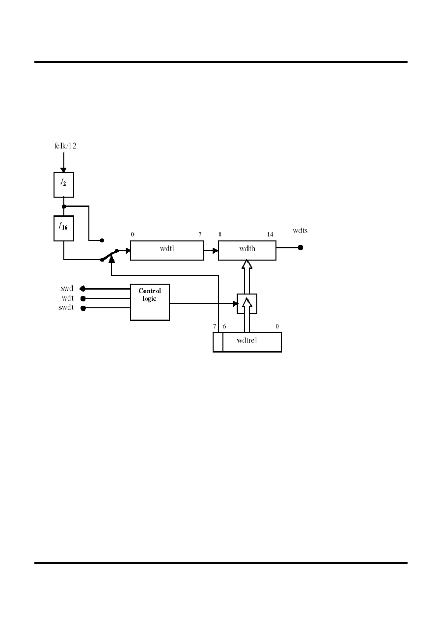
8.4. Watchdog Timer
The watchdog timer is a 16-bit counter that is incremented once every 24 or 384 clock cycles. After an external reset the
watchdog timer is disabled and all registers are set to zeros.
Watchdog Timer structure
The watchdog consists of 16-bit counter wdt, reload register wdtrel, prescalers by 2 and by 16 and control logic.
Watchdog block diagram
Start procedure
There are two ways to start the watchdog. One method, called hardware automatic start, is based on examining the level of
signal swd during active internal rst signal. When this condition is met, the watchdog will start running automatically with
default settings (all registers set to zeros).When this criterion is not met during active internal rst signal, a programmer can
start the watchdog later. It will occur when signal swd becomes active. Once the watchdog is started it cannot be stopped
unless internal rst signal becomes active. When wdt registers enters the state 7CFFh , asynchronous wdts signal will become
active. The signal wdts sets the bit 6 in ip0 register and requests reset state. The wdts is cleared either by rst signal or change
of the state of the wdt timer.
Refreshing the watchdog timer
The watchdog timer must be refreshed regularly to prevent reset request signal from becoming active. This requirement
imposes obligation on the programmer to issue two followed instructions. The first instruction sets wdt and the second one
swdt. The maximum allowed delay between settings of the wdt and swdt is 12 clock cycles. While this period has expired
and swdt has not been set, wdt is automatically reset, otherwise the watchdog timer is reloaded with the content of the wdtrel
register and wdt is automatically reset.

TE
CH
tm
T81L0003B
TM Technology Inc. reserves the right P. 11 Publication Date: NOV. 2005
to change products or specifications without notice. Revision:A
Special Function Registers
a) Interrupt Enable 0 register (ien0)
The ien0 register (address : A8)
MSB
LSB
eal wdt et2 es0 et1 ex1 et0 ex0
The ien0 bit functions
Bit Symbol
Function
ien0.6 wdt
Watchdog timer refresh flag.
Set to initiate a refresh of the watchdog timer. Must be set directly before swdt is set to prevent
an unintentional refresh of the watchdog timer. The wdt is reset by hardware 12 instruction
cycles after it has been set.
Note: other bits are not used to watchdog control
The ien0 bit functions
b) Interrupt Enable 1 register (ien1)
The ien1 register (Address : B8)
MSB
LSB
- swdt pt2 ps pt1 px1 pt0 px0
The ien1 bit functions
Bit Symbol
Function
Ien1.6 swdt
Watchdog timer start refresh flag.
Set to active/refresh the watchdog timer. When directly set after setting wdt, a watchdog timer
refresh is performed. Bit swdt is reset by hardware 12 instruction cycles after it has been set.
Pay attention that when write ien1.6, it write the swdt bit, when read ien1.6, we will read out the wdts bit. Ie. Watch dog
timer status flag. Set by hardware when the watchdog timer was started.
c) Watchdog Timer Reload register (wdtrel)
The wdtrel register ( Address : 86 )
MSB
LSB
7 6 5 4 3 2 1 0
The wdtrel bit functions
Bit Symbol
Function
wdtrel.7 7
Prescaler select bit. When set, the watchdog is clocked through an additional
divide-by-16 prescaler
wdtrel.6 t0
wdtrel.0
6-0
Seven bit reload value for the high-byte of the watchdog timer. This value is loaded
to the wdt when a refresh is triggered by a consecutive setting of bits wdt and swdt
The wdtrel register can be loaded and read any time

TE
CH
tm
T81L0003B
TM Technology Inc. reserves the right P. 12 Publication Date: NOV. 2005
to change products or specifications without notice. Revision:A
WDT Reset
A high on reset pin or watchdog reset request for two clock cycles while the oscillator is running resets the device.
Diagram
Reset timing
a) External hardware reset
Figure External reset timing
**Note:
clk: external clock input
Tclk: clock period
reset: external reset input
rst: internally generated reset signal
b) Watchdog timer reset
Figure Watchdog reset timing
**Note:
clk: external clock input
Tclk: clock period
wdt: watchdog timer registers
wdts: watchdog timer status flag
reset: external reset input
rst: internally generated reset signal

TE
CH
tm
T81L0003B
TM Technology Inc. reserves the right P. 13 Publication Date: NOV. 2005
to change products or specifications without notice. Revision:A
9. Timing Diagram
S1.........S
6
S1.........S
6
S1.........S
6
S1.........S
6
S1.........S
6
S1.........S
6
S1.........S
6
S1.........S
6
S1.........S
6
S1.........S
6
ALE
D0
D1
D2
D3
D4
D5
D6
D7
RXD
TXD
D0
D1
D2
D3
D4
D5
D6
D7
RXD
TXD
Receive
Shift
Write to SCON, Clear RI
RI
Re
ce
i
v
e
Write to SBUF
Send
Shift
Serial Port Mode 0
Tr
a
n
s
m
i
t

TE
CH
tm
T81L0003B
TM Technology Inc. reserves the right P. 14 Publication Date: NOV. 2005
to change products or specifications without notice. Revision:A
TX
D0
D1
D2
D3
D4
D5
D6
D7
TXD
TI
Shift
RI
Re
c
e
i
v
e
Write to SBUF
Send
Shift
Serial Port Mode 1
Tr
a
n
s
m
i
t
Stop
Bit
Data
Start
Bit
RX
D0
D1
D2
D3
D4
D5
D6
D7
RXD
Stop
Bit
Start
Bit
TX
D0
D1
D2
D3
D4
D5
D6
D7
TXD
TI
Shift
RI
Re
c
e
i
v
e
Write to SBUF
Send
Shift
Serial Port Mode 2 & 3
T
r
an
s
mit
Stop Bit
Data
Start
Bit
RX
D0
D1
D2
D3
D4
D5
D6
D7
RXD
Stop Bit
Start
Bit
TB8
TB8

TE
CH
tm
T81L0003B
TM Technology Inc. reserves the right P. 15 Publication Date: NOV. 2005
to change products or specifications without notice. Revision:A
Package Dimension
18-LEAD SOP
E
H
1
10
18
9
0.016typ
0.050typ
0.020X45
A
A1
D
0.004max
L
X
SYMBOLS
MIN.
MAX.
A 0.093
0.104
A1 0.004 0.012
D 0.447
0.463
E 0.291
0.229
H 0.394
0.419
L 0.016
0.050
X 0 8
UNIT: INCH

TE
CH
tm
T81L0003B
TM Technology Inc. reserves the right P. 16 Publication Date: NOV. 2005
to change products or specifications without notice. Revision:A
18-LEAD DIP
1
10
18
9
0.018 +-
0.012 Typ.
0.100
Typ.
R40
A +- 10
0.
290
+
-
0.
01
4
0.
312
+
-
0.
01
2
0.310 M ax
D +- 14
C +- 14
0.
350 +
-
0.
020
0.
115
M
in.
B +-
0.020
E +-
0.020
0.060 +-
0.015 Typ.
0.
015 M
i
n.
A
B
C
D
E
0.900 0.075 0.065 0.055 0.090
UNIT: INCH