 | –≠–ª–µ–∫—Ç—Ä–æ–Ω–Ω—ã–π –∫–æ–º–ø–æ–Ω–µ–Ω—Ç: T8246A-D | –°–∫–∞—á–∞—Ç—å:  PDF PDF  ZIP ZIP |
TE
CH
tm
Preliminary T8246A
TM Technology Inc. reserves the right P. 1
Publication Date: OCT. 2002
to change products or specifications without notice.
Revision:0.A
T8246A
Touch Screen Controller
Features
! Single Supply Vcc of 2.2V to 5.25V.
! Direct Battery Measurement (0V~6V).
! Shutdown Mode:1uA Max.
! 4-Wire Touch Screen Interface.
! Up to 125KHz conversion rate.
! Internal 2.5V Reference.
! On-chip temperature measurement
! Touch-pressure measurement.
! Ratio metric Conversion
! One Auxiliary Analog Input
! Programmable 8 or 12 Bit Resolution
Application
! Personal digital assistants,(PDAs)
! Point-of-sales terminals
! Touch-screen monitors,(e-Book)
! Cellular phones.
! Smart Hand-Held Devices.
Part Number Examples
Part NO.
Pkg.
Description
T8246A-D SSOP SSOP-16Pin
T8246A-P TSSOP
TSSOP-16Pin
Description
The T8246A is an industry standard 4-wire touch screen
controller. It contains a 12-bit successive approximation
analog to digital converter (ADC) with a synchronous
serial interface and low on-resistance switches for
driving touch screens. This allows for easy upgrade for
current applications with the new version MCU. Only
software changes will be required to take advantage of
the added features of direct battery measurement,
temperature measurement, and touch-pressure
measurement. The T8246A also has an on-chip 2.5V
reference that can be utilized for the auxiliary input,
battery monitor, and temperature measurement modes.
The reference can also be powered down when not used
to conserve power. The internal reference will operate
down to 2.7V supply voltage while monitoring the
battery voltage from 0V to 6V.
The low power consumption of < 0.5mW typ. at 2.7V
(internal reference OFF), high speed (> 125kHz clock
rate) and on-chip drivers make the T8246A an ideal
choice for battery-operated systems such as Personal
Digital Assistants (PDAs) with resistive touch screens,
pagers, cellular phones, and other portable equipment. It
guaranteed over the -40
o
C to +85
o
C operating
temperature range.
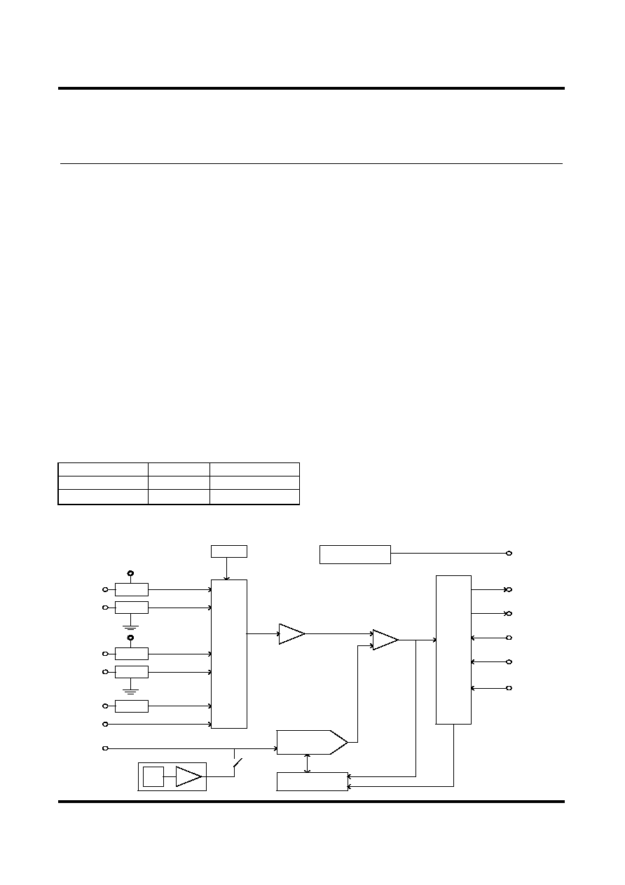
Block Diagram
PMOS
SWITCH
NMOS
SWITCH
PMOS
SWITCH
NMOS
SWITCH
Battery
monitor
X+
X-
Y+
VBAT
VDD
GND
VDD
GND
TEMP
SENSOR
6 TO 1
ANALOG
INPUT
MUX
2.5V
REF
Buffer
AUX
Comp
S/H
CHARGE
REDISTRIRUTION
DAC
SAR+ADC
CONTROL LOGIC
SERIAL
DATA
INPUT
OUTPUT
CONTROL
LOGIC
BUSY
DOUT
/CS
DCLK
DIN
PEN
INTERRUPT
/PENIRQ
VREF
VIN
Y-

TE
CH
tm
Preliminary T8246A
TM Technology Inc. reserves the right P. 2
Publication Date: OCT. 2002
to change products or specifications without notice.
Revision:0.A
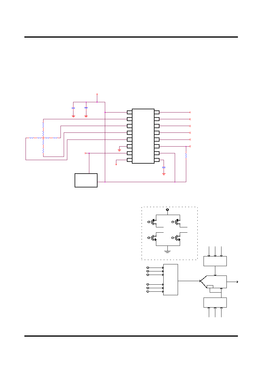
Pin Configurations
+VCC
VREF
DOUT
BUSY
DIN
/CS
DCLK
/PENIRQ
Y+
X+
+VCC
Y-
GND
X-
VBAT
AUX
TSSOP
&
SSOP
Top View
16
15
14
13
12
11
10
9
1
2
3
4
5
6
7
8
Pin description
Pin No.
Symbol Pin description
1
+VCC
Positive Supply Voltage. Connect with pin10.
2
X+
X+ Position Input. ADC Input Channel 1.
3
Y+
Y+ Position Input. ADC Input Channel 2.
4
X-
X≠ Position Input.
5
Y-
Y≠ Position Input.
6 GND
Ground.
7 V
BAT
Battery Monitor input.
8
AUX
Auxiliary Input . ADC Input channel 4.
9 V
REF
Voltage Reference Input/output.
10
+VCC
Positive supply Voltage. +2.2V to +5.25V. External (internal) reference. Bypass with a 1uF
capacitor. Connect with pin1 *
note1
11
/PENIRQ Pen Interrupt. Open drain output (requires 10K to 100K pull-up resistor externally).
12
DOUT
Serial Data Output. Data is shifted on the falling edge of DCLK. This output is high impedance
when /CS is HIGH.
13
BUSY
Busy Output. This output is high impedance when /CS is HIGH.
14
DIN
Serial Data Input. If /CS is LOW, data is latched on rising edge of DCLK.
15
/CS
Chip Select Input. Controls conversion timing and enables the serial input/output register.
16
DCLK
External Clock Input. This clock runs the SAR conversion process and synchronizes serial data I/O.
Note : 1.The T8246A is guaranteed to operate with a supply voltage down to +2.2V when used with an external
reference or +2.7V with an internal reference.

TE
CH
tm
Preliminary T8246A
TM Technology Inc. reserves the right P. 3
Publication Date: OCT. 2002
to change products or specifications without notice.
Revision:0.A
Electrical Characteristic
At Ta=-40C to 85C, Vcc=2.7V,Fsclk=2.0MHZ(external clock 50% duty cycle, Fck=16*Fsample=2MHz) 15clocks / conversion
cycle(133kdps); T8246A-4.7uF capacitor at V
REF
pin;T8246A-external reference,(V
REF
=2.5000V applied to V
REF
pin),
Fsample=125KHz, 12-bit mode, and digital inputs=GND or Vcc, unless otherwise noted.
Parameter Conditions
Min.
Typ.
Max.
Units
Analog input
Input Voltage Ranges
Input Capacitance
DC Leakage current
-
-
-
0
-
-
-
37
±
0.1
V
REF
-
-
V
pF
uA
System performance
Resolution
No missing codes
Integral Nonlinearity.
Offset Error
Gain Error
Noise
Power supply rejection
+VCC=2.7V
External Reference.
-
11
-
-
-
-
-
12
-
-
-
-
70
70
-
-
±
2
±
6
±
4
-
-
Bits
Bits
LSB
LSB
LSB
uVrms
dB
Conversion rate
Conversion time
Acquisition time
Throughput rate
-
3
-
-
-
-
12
-
125
CLK cycles
CLK cycles
KHz
Switch Driver
On-Resistance.
Y+,X+
Y-,X-
-
-
5
6
-
-
Reference Input/Output
Internal Reference Voltage
Internal Reference Temp. coefficient
V
REF
input Voltage Range
DC Leakage Current
V
REF
input Impedance
/CS=GND or +VCC; Typically 260 when
on-board Reference Enabled.
2.45
-
1
-
-
2.50
15
-
-
1
2.55
-
VCC
±
1
-
V
ppm/
o
C
V
uA
G
Battery Monitor
Input Voltage Range
Input Impedance
Accuracy
Sampling; 1G when Battery Monitor OFF
External Reference
Internal Reference
0
-
-
-
-
10
-
-
6
-
±
2.5
±
3
V
K
%
%
Logic Input
Input High Voltage, V
IH
Input Low Voltage, V
IL
Input Current, I
IN
Input Capacitance, C
IN
*Note
1
Typically 10nA,VIN =0V or +VCC
2.4
-
-
-
-
-
-
-
-
0.4
±
1
10
V
V
uA
pF
Logic Output
Output High Voltage, V
OH
Output Low Voltage, V
OL
/PENIRQ Output Low Voltage,
Floating-State Leakage Current
Floating-State Output Capacitance *Note
1
Output Coding
Isource=250uA;VCC=2.2 to 5.25V
Isink=250uA
100k Pull-UP; Isink=250uA
Straight(Natural)Binary
VCC-0.2
-
-
-
-
-
-
-
-
-
-
0.4
0.4
±
10
10
V
V
V
uA
pF
Temperature Measurement
Temperature Range
Resolution
Accuracy
Differential Method *Note
2
Single Conversion Temp0 *Note
3
Differential Method *Note
2
Single Conversion Temp1 *Note
3
-40
-
-
-
-
-
1.6
0.3
±
2
±
2
+85
-
-
-
-
o
C
o
C
o
C
o
C
o
C
TE
CH
tm
Preliminary T8246A
TM Technology Inc. reserves the right P. 4
Publication Date: OCT. 2002
to change products or specifications without notice.
Revision:0.A
Power supply requirements Vcc Specified
performance
Operation Range
2.70
2.2
-
-
3.60
5.25
V
V
Internal Reference OFF
VCC=3.6V,240uA typ
- - 380
uA
Fsample =125kHZ
Internal Reference ON
VCC=3.6V
- 670 -
uA
Internal Reference OFF
VCC=2.7V,f
DCK
=200kHZ
- 170 -
uA
Internal Reference OFF
VCC=3.6V
- 150 -
uA
Fsample
=12.5kHZ
Internal Reference ON
VCC=3.6V
- 580 -
uA
Quiescent Current
Supply Current
-
Shut Down Mode
with DCLK=DIN =+VCC
- 1 -
uA
Fsample =125kHZ
VCC=3.6V.Internal Reference Disabled
VCC=3.6V.Internal Reference Enabled
-
-
-
2.412
1.368
-
mW
mW
Power dissipation
- Shutdown
(VCC=3.6V)
-
-
3.6
uW
Note : 1. Sample tested on 25
o
C to ensure compliance.
2. Differential Method between Temp0 and Temp1 measurement. No calibration necessary.
3. Temperature drift is ≠2.1mV/
o
C
Circuit Information
The T8246A is a fast, low-power, 12-bit, single supply
A/D converter. The T8246A can be operated from a 2.2
V to 5.25 V supply. When operated from either a 5 V
supply or a 3 V supply, It is capable of throughput rates
up to 125 kHz when provided with a 2 MHz clock. The
T8246A provides the user with an on-chip track/hold,
multiplexer.A/D converter, reference, temperature sensor,
and serial interface housed in a tiny 16-lead SSOP,
TSSOP, package, which offers the user considerable
space-saving advantages over alternative solutions. The
serial clock input (DCLK) accesses data from the part but
also provides the clock source for the successive
approximation A/D converter. The analog input range is
0 V to V
REF
(where the externally applied V
REF
can be
between 1V to +VCC ). The T8246A has a 2.5 V
reference on chip! with this reference voltage available
for use externally if buffered. The analog input to the
ADC is provided via an on-chip multiplexer. This analog
input may be any one of the X, Y, and Z panel
coordinates, battery voltage, or chip temperature. The
multiplexer is configured with low resistance switches
that allow an unselected ADC input channel to provide
power and an accompanying pin to provide ground for an
external resistive touch screen device. For some
measurements the on resistance of the switches may
present a source of error, However, with a differential
reference to the converter, That the error can be negated.
The T8246A is guaranteed to operate with a supply
voltage down to +2.2V when used with an external
reference or +2.7V with an internal reference. In
shut-down mode, the typical power consumption is
reduced to under 0.5uW, while the typical power
consumption at 125kHZ throughput and a +2.7V supply
is 650uW
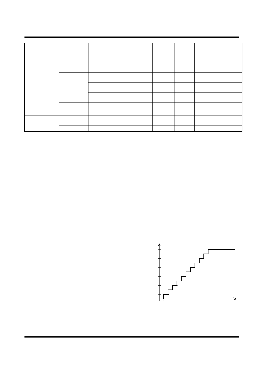
ADC Transfer Function
The output coding of the T8246A is straight binary. The
designed code transitions occur at successive integer
LSB values (i.e.,1 LSB, 2 LSBs, etc.). The LSB size is =
V
REF
/4096. The ideal transfer characteristic for the
T8246A is shown in Figure 1
000...000
000...001
000...010
...
...
011...111
...
111...111
111...110
...
...
111...000
~ ~
~
~
~ ~
0V 1LSB
+VREF-1LSB
ANALOG INPUT
ADC CODE
1LSB=VREF/4096
Figure1. Transfer Characteristic
TE
CH
tm
Preliminary T8246A
TM Technology Inc. reserves the right P. 5
Publication Date: OCT. 2002
to change products or specifications without notice.
Revision:0.A
Typical Connection Diagram
Figure 2 shows a typical connection diagram for the
T8246A in a resistive touch screen control application.
The T8246A features an internal reference but this can be
overdriven with an external low impedance source
between 1V and +VCC. The value of the reference
voltage will set the input range of the converter. The
conversion result is output MSB first, followed by the
remaining 11 bits and three trailing zeroes, depending on
the number of clocks used per conversion (see the Serial
Interface section). For applications where power
consumption is major concern, the power management
option should be used to improve power performance.
See Table III for available power management options.
2
12
Chip Select
Serial Data Out
AUX
VREF
3
Y+
10
Y+
DOUT
4
0.1uF
BUSY
5
1uF~10uF
Auxiliary
DIN
VBAT
6
Pen Interrupt
Touch
/CS
7
Screen
+2.2V to +5V
8
0.1uF
9
DCLK
Serial conversion Clock
Regulator
Converter Status
11
/PENIRQ
100K
Voltage
T8246A
Input
X-
13
Serial Data In
To Battery
GND
14
Y-
Y-
1
15
X-
+VCC
16
X+
(Optional)
X+
+VCC
Figure 2. Typical Application Circuit
Analog Input
Figure3 shows an equivalent circuit of the analog input
structure of the T8246A that contains a block diagram of
the input multiplexer, the input of the A/D converter, and
the differential reference. Table1 shows the multplexer
address corresponding to each analog input, both for the
SER/DFR bit in the control register set high and low. The
control bits are provided serially to the device via the
DIN pin. For more information on the control register,
see the Control Register section. When the converter
enters the hold mode, the voltage difference between the
+IN and -IN inputs (see Figure 3) is captured on the
internal capacitor array. The input current on the analog
inputs depends on the conversion rate of the device.
During the sample period, the source must charge the
internal sampling capacitor (typically 37pF). Once the
capacitor has been fully charged, there is no further input
current. The rate of charge transfer from the analog
source to the converter is a function of conversion rate.
IN+
Y-
MUX
6 TO 1
Y+
X+
AUX
VBAT
TEMP
IN-
REF-
IN+
REF+
ADC CORE
MUX
3 TO 1
MUX
3 TO 1
X+
Y+
REF
INT/EXT
Y-
X-
GND
GND
VCC
X+
Y+
Y-
X-
ON-CHIP SWITCHES
DATA
OUT
Figure3 Equivalent Analog Input Circuit.

TE
CH
tm
Preliminary T8246A
TM Technology Inc. reserves the right P. 6
Publication Date: OCT. 2002
to change products or specifications without notice.
Revision:0.A
A2 A1 A0 SER/DFR
Analog IN
X Switches
Y Switches
+REF
*note1
-REF
*note1
0
0
0
0
0
1
1
1
TEMP0
X+
OFF
OFF
OFF
ON
V
REF
V
REF
0 1 0
1 V
BAT
OFF OFF V
REF
X+ OFF
Y+ ON
V
REF
0 1 1
1 X+(Z1)
X- ON
Y- Off
X+ OFF
Y+ ON
V
REF
1 0 0
1 Y-(Z2)
X- ON
Y- OFF
GND
GND
GND
GND
GND
1 0 1
1 Y+
ON
OFF V
REF
GND
1 1 0
1 AUX
OFF
OFF
V
REF
GND
1 1 1
1 TEMP1
OFF
OFF
V
REF
GND
0 0 0
0
Invalid address. Test Mode: Switches out the Temp0 diode to the /PENIRQ pin
0 0 1
0 X+
OFF
ON
Y+
Y-
0 1 0
0 Invalid
address.
X+ OFF
Y+ ON
Y+
X-
0 1 1
0 X+(Z1)
X- ON
Y- OFF
X+ OFF
Y+ ON
Y+
X-
1 0 0
0 Y-(Z2)
X- ON
Y- OFF
1 0 1
0 Y+
ON
OFF
X+
X-
1 1 0
0
1 1 1
0
Outputs Identity Code,1000 0000 0000.
Invalid address. Test mode: Switches out the TEMP0 diode to the /PENIRQ pin.
*Note1:Internal Node, Not Directly accessible by the user.
Table1. analog Input ,Reference, and Touch Screen Control.
Acquisition Time
The track-and-hold amplifier enters its tracking mode on
the falling edge of the fifth DCLK after the START bit
has been detected. The time required for the track-and
hold amplifier to acquire an input signal will depend on
how quickly the 37pF input capacitance is charged. With
zero source impedance on the analog input, three DCLK
cycles will always be sufficient to acquire the signal to
the 12-bit level. With a source impedance R
IN
on the
analog input, the actual acquisition time required is
calculated using the formula:
t
ACQ
= 8.4*(R
IN
+ 100
) *37pF
Where R
IN
is the source impedance of the input signal,
and 100
, 37pF is the input RC. Depending on the
frequency of DCLK used, three DCLK cycles may or
may not be sufficient to acquire the analog input signal
with various source impedance values.
Touch Screen Settling
In some applications, external capacitors may be required
across the touch screen to filter noise associated with it,
e.g., noise generated by the LCD panel or backlight
circuitry. The value of these capacitors will cause a
settling time requirement when the panel is touched. The
settling time will typically show up as a gain error. There
are several methods for minimizing or eliminating this
issue. The problem may be that the input signal,
reference, or both, have not settled to their final value
before the sampling instant of the ADC. Additionally, the
reference voltage may still be changing during the
conversion cycle. One option is to stop, or slow down,
the DCLK for the required touch screen settling time.
This will allow the input and reference to stabilize for the
acquisition time. This will resolve the issue for both
single-ended and differential modes.
The other option is to operate the T8246A in differential
mode only for the touch screen, and program the T8246A
keep the touch screen drivers on and not go into
power-down (PD0 = PD1 = 1). Several conversions may
be required, depending on the settling time required and
the T8246A data rate. Once the required number of
conversions have been made, The T8246A can then be
placed in a power-down state on the last measurement.
The last method is to use the 15 DCLK cycle mode
which maintains the touch screen drivers on until it is
commanded by the processor to stop.

TE
CH
tm
Preliminary T8246A
TM Technology Inc. reserves the right P. 7
Publication Date: OCT. 2002
to change products or specifications without notice.
Revision:0.A
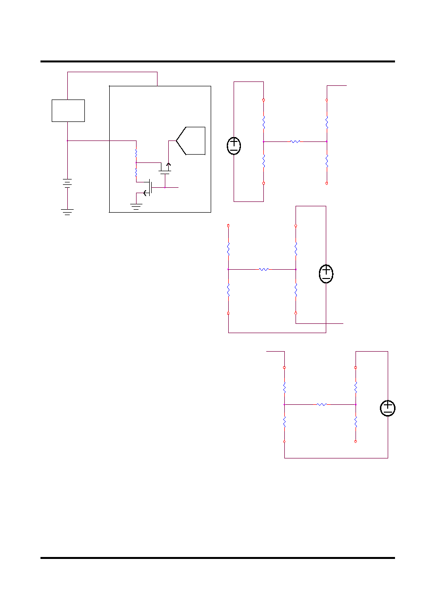
Internal Reference
The T8246A has an internal reference voltage of 2.5 V.
The internal reference is available on the V
REF
pin for
external use in the system; however, it must be buffered
before it is applied elsewhere. The on-chip reference can
be turned ON or OFF with the power-down address, PD1
= 1 (see Table3 and Figure4). Typically the reference
voltage is only used in the single-ended mode for battery
monitoring, temperature measurement, and for using the
auxiliary input. Optimal touch screen performance is
achieved when using the differential mode. The power-up
time of the 2.5 V reference is typically 10us without a
load; however, a 0.1uF capacitor on the V
REF
pin is
recommended for optimum performance, which will
affect the power-up time.
VREF
Reference
To CDAC
Band
Gap
Buffer
Optional
Power Down
SW1
Figure4. On-Chip Reference Circuitry
Reference Input
The voltage difference between +REF and -REF (see
Figure3) sets the analog input range. The T8246A will
operate with a reference input in the range of 1V to
+VCC. Figure4 shows the on-chip reference circuitry on
the T8246A. The internal reference on the T8246A can
be overdriven with an external reference; for best
performance, however, the internal reference should be
disabled when an external reference is applied, as SW1 in
Figure4 will open on the T8246A when the internal
reference is disabled. The on-chip reference will always
be available at the V
REF
pin as long as the reference is
enabled. The input impedance seen at the V
REF
pin is
approximately 260
when the internal reference is
enabled. When it is disabled, the input impedance seen at
the V
REF
pin will be in the giga ohm region.
When making touch screen measurements, conversions
can be made in the differential (ratiometric) mode or the
single-ended mode. If the SER/DFR bit is set to high in
the control register, then a single-ended conversion will
be performed. Figure5 shows the configuration for a
single-ended Y coordinate measurement. The X+ input is
connected to the analog-to-digital converter, the Y+ and
Y-- drivers are turned on, and the voltage on X+ is
digitized. The conversion is performed with the ADC
referenced from GND to V
REF
. This V
REF
will either be
the on-chip reference or the voltage applied at the V
REF
pin externally, and is determined by the setting of the
power management bits PD0 and PD1 (see Table2). The
advantage of this mode is that the switches that supply
the external touch screen can be turned off once the
acquisition is completed, resulting in power savings.
However, the on resistance of the Y drivers will affect
the input voltage that can be acquired. The full touch
screen resistance may be in the order of 200
to 900
,
depending on the manufacturer. Thus, if the on resistance
of the switches is approximately 6
, then true full-scale
and zero-scale voltages cannot be acquired, regardless of
where the pen/stylus is on the touch screen. Note, the
minimum touch screen resistance recommended for use
with the T8246A is approximately 70
. In this mode of
operation, therefore, some voltage is likely to be lost
across the internal switches and it is unlikely that the
internal switch resistance will track the resistance of the
touch screen over temperature and supply, providing an
additional source of error.
+VCC
REF-
X+
ADC CORE
IN+
Y+
REF+
IN-
Y-
GND
IN+
VREF
Figure5. Single-Ended Reference Mode (SER/DFR=H)

TE
CH
tm
Preliminary T8246A
TM Technology Inc. reserves the right P. 8
Publication Date: OCT. 2002
to change products or specifications without notice.
Revision:0.A
The alternative to this situation is to set the SER/DFR bit
low. Again, making a Y coordinate measurement is
considered, but now the +REF and -REF nodes of the
ADC are connected directly to the Y+ and Y- pins. This
means the analog-to-digital conversion will be
ratiometric. The result of the conversion will always be a
percentage of the external resistance, independent of how
it may change with respect to the on resistance of the
internal switches. Figure6 shows the configuration for a
ratiometric Y coordinate measurement.
Y+
+VCC
ADC CORE
GND
IN-
X+
Y-
REF-
REF+
IN+
IN+
Figure6.Differential Reference Mode (SER/DFR=0)
The disadvantage of this mode of operation is that during
both the acquisition phase and conversion process, the
external touch screen must remain powered. This will
result in additional supply current for the duration of the
conversion.
Temperature Measurement
Two temperature measurement options are available on
the T8246A, the single conversion method and the
differential conversion method. Both methods are based
on an on-chip diode measurement. In the single
conversion method, a diode voltage is digitized and
recorded at a fixed calibration temperature. Any
subsequent polling of the diode will provide an estimate
of the ambient temperature through extrapolation from
the calibration temperature diode result. This assumes a
diode temperature drift of approximately -2.1mV/
o
C.
This method provides a resolution of approximately
0.3
o
C and a predicted accuracy of
±
3
o
C.
The differential conversion method is a two-point
measurement. The first measurement is performed with a
fixed bias current into a diode and the second
measurement is performed with a fixed multiple of the
bias current into the same diode. The voltage difference
in the diode readings is proportional to absolute
temperature and is given by the following formula:
∑
V
BE
= (kT/q)*(ln N)
where V
BE
represents the diode voltage, N is the bias
current multiple, k is Boltzmann's constant and q is the
electron charge. This method provides more accurate
absolute temperature measurement of
±
2
o
C. However,
the resolution is reduced to approximately 1.6
o
C .
Assuming a current multiple of 91(which is typical for
the T8246A) taking Boltzmann's constant, k = 1.38054
*10
-23
electrons volts/degrees Kelvin, the electron charge
q = 1.602189*10
-19
, then T, the ambient temperature in
degrees centigrade, would be calculated as follows:
V
BE
= (kT/q )* (ln N)
T=(V
BE
* q) / (k*ln N)
T
o
C = 2.573*10
3
*V
BE
≠ 273
o
K
V
BE
is calculated from the difference in readings from the
first conversion and second conversion. Figure7 shows a
block diagram of the temperature measurement mode.
ADC
MUX
TEMP 0 TEMP 1
I
91*I
Figure7.Block Diagram of Temperature Measurement Circuit
Battery Measurement
The T8246A can monitor a battery voltage from 0 V to 6
V. Figure8 shows a block diagram of a battery voltage
monitored through the V
BAT
pin. The voltage to the
+VCC of the T8246A is maintained at the desired supply
voltage via the dc/dc regulator while the input to the
regulator is monitored. This voltage on V
BAT
is divided
by 4 so that a 6 V battery voltage is presented to the
ADC as 1.5 V. To conserve power, the divider is only on
during the sampling of a voltage on V
BAT
. Table1 shows
the control bit settings required to perform a battery
measurement.
TE
CH
tm
Preliminary T8246A
TM Technology Inc. reserves the right P. 9
Publication Date: OCT. 2002
to change products or specifications without notice.
Revision:0.A
7.5K
2.5K
+VCC
Converter
0V to 1.5V
VBAT
Battery
0V to 6V
DC / DC
+
-
ADC CORE
Figure8. Block Diagram of Battery Measurement Circuit
Pressure Measurement
The pressure applied to the touch screen via a pen or
finger may also be measured with the T8246A with some
simple calculations. The 8-bit resolution mode would be
sufficient for this measurement, but the following
calculations are shown with the 12-bit resolution mode.
The contact resistance between the X and Y plates is
measured. This provides a good indication of the size of
the depressed area and the applied pressure. The area of
the spot touched is proportional to the size of the object
touching it. The size of this resistance (R
TOUCH
) can be
calculated using two different methods. The first method
requires the user to know the total resistance
of the X-plate tablet. Three touch screen conversions are
required, a measurement of the X-position, Z
1
-position
and Z
2
≠position (see Figure 9). The following equation
will calculate the touch resistance:
R
TOUCH
= (R
XPLATE
) *(X
POSITION
/4095)*[(Z
2
/Z
1
) -1]
The second method requires that the resistance of both
the X-plate and Y-plate tablets are known. Again three
touch screen conversions are required, a measurement of
the X-position, Y-position, and Z
1
-position (see Figure
9)The following equation will also calculate the touch
resistance:
R
TOUCH
= {(R
XPLATE
/Z
1
)*(X
POSITION
/4095)*[(4096/Z
1
) -
1]}-{R
YPLATE
*(Y
POSITION
/4095)}
X+
Y+
Y-
X-
X-Position
Touch
Measure
X-Position
Y+
Y-
X+
X-
Z2-Position
Measure
Z2-Position
Touch
X+
Y+
Y-
X-
Z1-Position
Touch
Measure
Z1-Position
Figure9. Pressure Measurement Block Diagrams.
Pen Interrupt Request
The pen interrupt equivalent output circuitry is outlined
in Figure10. By connecting a pull-up resistor (10k
to
100k
) between +VCC and open drain output, the
/PENIRQ output will remain high normally. If /PENIRQ
has been enabled (see Table3), when the touch screen

TE
CH
tm
Preliminary T8246A
TM Technology Inc. reserves the right P. 10
Publication Date: OCT. 2002
to change products or specifications without notice.
Revision:0.A
connected to the T8246A is touched by a pen or finger,
the /PENIRQ output will go low, initiating an interrupt to
a microprocessor that may then instruct a control word to
be written to the T8246A to initiate a conversion. This
output can also be enabled between conversions during
power-down (see Table3) allowing power-up to be
initiated only when the screen is touched. The result of
the first touch screen coordinate conversion after
power-up will be valid assuming any external reference is
settled to the 12- or 8-bit level as required.
/PENIRQ
100K
Y+
X+
Y-
ON
/PENIRQ
ENABLE
TOUCH
SCREEN
EXTERNAL
PULL-UP
+VCC
+VCC
Figure10. /PENIRQ Functional Block Diagram.
~
t
8
1
~
16
~
S
SCREEN
PEN
DFR#
~
TOUCHED
INTERRUPT
SER/
HERE
(START)
PD1=1 , PD0=0 , /PENIRQ
13
1
DCLK
MOD
PROCESSOR
/PENIRQ
A0
~
DIN
~
1
A2
0
/CS
A1
~
ENABLED AGAIN
NO RESPONSE TO TOUCH
~
Figure11. /PENIRQ Timing Diagram
Figure11 assumes the /PENIRQ function has been
enabled in the last write or the part has just been powered
up so /PENIRQ is enabled by default. Once the screen is
touched, the /PENIRQ output will go low a time t
PEN
later. This delay is approximately 5us, assuming a 10nF
touch screen capacitance, and will vary with the touch
screen resistance actually used. Once the START bit is
detected the pen interrupt function is disabled and the
/PENIRQ will not respond to screen touches. The
/PENIRQ output will remain low until the fourth falling
edge of DCLK after the START bit has been clocked in,
at which point it will return high as soon as possible,
irrespective of the touch screen capacitance. This does
not mean the pen interrupt function is now enabled again
as the power-down bits have not yet been loaded to the
control register. So regardless of whether /PENIRQ is to
be enabled again, the /PENIRQ output will always idle
high normally. Assuming the /PENIRQ is enabled again
as shown in Figure11, then once the conversion is
complete, the /PENIRQ output will again respond to a
screen touch. The fact that /PENIRQ returns high almost
immediately after the fourth falling edge of DCLK means
the user will avoid any spurious interrupts on the
microprocessor or DSP that could occur if the interrupt
request line on the MCU/DSP were unmasked during or
toward the end of conversion and the /PENIRQ pin was
still low. Once the next START bit is detected by the
T8246A the /PENIRQ function is again disabled. If the
control register write operation will overlap with the data
read, a START bit will always be detected prior to the
end of conversion, meaning that even if the /PENIRQ
function has been enabled in the control register it will be
disabled by the START bit again before the end of the
conversion is reached, so the /PENIRQ function
effectively cannot be used in this mode. How-ever, as
conversions are occurring continuously, the /PENIRQ
function is not necessary and is therefore redundant.
Control Register
The control word provided to the ADC via the DIN pin is

TE
CH
tm
Preliminary T8246A
TM Technology Inc. reserves the right P. 11
Publication Date: OCT. 2002
to change products or specifications without notice.
Revision:0.A
shown in Table2. This provides the conversion start,
channel addressing, ADC conversion resolution,
configuration, and power-down of the T8246A. Table2
provides detailed information on the order and
description of these control bits within the control word.
Initiate START
The first bit, the "S" bit, must always be set to 1 to
initiate the start of the control word. The T8246A will
ignore any inputs on the DIN line until the start bit is
detected.
Channel Addressing
The next three bits in the control register, A2, A1, and
A0, select the active input channel(s) of the input
multiplexer (see Table1 and Figure3), touch screen
drivers, and the reference inputs.
MODE
The MODE bit sets the resolution of the analog-to-digital
converter. With a 0 in this bit, the following conversion
will have 12 bits resolution. With a 1 in this bit, the
following conversion will have 8 bits resolution.
SER/DFR
The SER/DFR bit controls the reference mode, which can
be either single-ended or differential if a "1" or a "0" is
written to this bit respectively. The differential mode is
also referred to as the ratiometric conversion mode. This
mode is optimum for X-position, Y-position, and
pressure-touch measurements. The reference is derived
from the voltage at the switch drivers, which is almost the
same as the voltage to the touch screen. In this case, a
separate reference voltage is not needed as the reference
voltage to the analog-to-digital converter is the voltage
across the touch screen. In the single-ended mode, the
reference voltage to the converter is always the difference
between the V
REF
and GND pins. See Table1 and
Figures3 through 6 for further information.
If X-position, Y-position, and pressure touch are
measured in the single-ended mode, an external reference
voltage or +VCC is required for maximum dynamic
range. The internal reference can be used for these
single-ended measurements, however a loss in dynamic
range will be incurred. If an external reference is used,
the T8246A should also be powered from the external
reference. As the supply current required by the device is
so low, a precision reference can be used as the supply
source to the T8246A. It may also be necessary to power
the touch screen from the reference which may require
5mA to 10mA. A REF19x voltage reference can source
up to 30mA and as such could supply both the ADC and
the touch screen. Care must be taken however, to ensure
that the input voltage applied to the ADC does not
exceed the reference voltage and hence the supply
voltage. See Absolute Maximum Ratings section.
NOTE: The differential mode can only be used for
X-position, Y-position, and pressure touch measurements.
All other measurements require the single-ended mode.
PD0 and PD1
The power management options are selected by
programming the power management bits, PD0 and PD1,
in the control register. Table3 summarizes the options
available and the internal reference voltage
configurations. The internal reference can be turned ON
or OFF independent of the analog-to-digital converter,
allowing power saving between conversions using the
power management options.
Bit 7 Bit 6 Bit 5 Bit 4 Bit 3
Bit 2
Bit 1 Bit 0
(MSB)
(LSB)
S A2 A1 A0 MODE
SER/DFR PD1 PD0
Bit Name
Description
7
S
The control word starts with the first high bit on
DIN. A new control word can start every fifteenth
DCLK cycle when in the 12-bit conversion mode
or every eleventh DCLK cycle when in 8-bit
conversion mode.
6-4 A2-A0 Channel select bits. Along with the SER/DFR bit,
these bits control the setting of the multiplexer
input, switches, and reference inputs, as detailed
in Table 1 & 2.
3
MODE 12-bit/8-bit conversion select bit. This bit
controls the number of bits for the following
conversion: 12 bits (LOW) or 8 bits (HIGH).
2 SER,
/DFR
Single-Ended/Differential Reference select bit.
Along with bits A2-A0, this bit controls the
setting of the muxtiplexer input, switches, and
reference inputs, as detailed in Table 1 & 2.
1-0 PD1-
PD0
Power down mode select bits. The two bits
decode the power-down mode of the T8246A as
shown in Table3.
Table2. Control Register Bit Function Description.

TE
CH
tm
Preliminary T8246A
TM Technology Inc. reserves the right P. 12
Publication Date: OCT. 2002
to change products or specifications without notice.
Revision:0.A
PD1 PD0 /PENIRQ Description
0
0
Enabled This configuration will result in immediate power-down of the on-chip reference as soon as PD1 is set to 0.
The ADC will only power down between conversions. When PD0 is set to 0 the conversion will be
performed first and the ADC will power down upon completion of that conversion (or upon the rising edge
of CS if it occurs first). At the start of the next conversion, the ADC instantly powers up to full power. This
means if the device is being used in the differential mode, or an external reference is used, there is no need for
additional delays to ensure full operation and the very first conversion is valid. The Y- switch is ON while in
power-down. When the device is performing differential table conversions, the reference and reference buffer
will not attempt to power up with bits PD1 and PD0 programmed in this way.
0
1
Enabled (Reference is OFF and ADC is ON)
This configuration will result in switching the reference OFF immediately and the ADC ON permanently.
When the device is performing differential table conversions, the reference and reference buffer will not
attempt to power up with bits PD1 and PD0 programmed in this way.
1
0
Enabled (Reference is ON and ADC is OFF)
This configuration will result in switching the reference ON and powering the ADC down between
conversions. The ADC will only power down between conversions. When PD0 is set to 0 the conversion will
be performed first and the ADC will power down upon completion of that conversion (or upon the rising
edge of CS if it occurs first). At the start of the next conversion, the ADC instantly powers up to full power.
There is no need for additional delays to ensure full operation as the reference remains permanently powered
up.
1
1
Disabled Device is always powered. Reference is ON and ADC is ON
This configuration will result in keeping the device always powered up. The reference and the ADC are ON.
Table3. Power Management Options.
Serial Interface
Figure12 shows the typical operation of the serial
interface of the T8246A. The serial clock provides the
conversion clock and also controls the transfer of
information to and from the T8246A.One complete
conversion can be achieved with 24 DCLK cycles.
The /CS signal initiates the data transfer and conversion
process. The falling edge of /CS takes the BUSY output
and the serial bus out of three-state. The first eight DCLK
cycles are used to write to the control register via the
DIN pin. The control register is updated in stages as each
bit is clocked in and once the converter has enough
information about the following conversion to set the
input multiplexer and switches appropriately, the
converter enters the acquisition mode and if required, the
internal switches are turned on. During the acquisition
mode the reference input data is updated. After the three
DCLK cycles of acquisition, the control word is complete
(the power management bits are now updated) and the
converter enters the conversion mode At this point the
track and hold goes into hold mode and the input signal
is sampled and the BUSY output goes high (BUSY will
return low on the next falling edge of DCLK). The
internal switches may also turn off at this point if in
single-ended mode, battery-monitor mode, or
temperature measurement mode.
The next 12 DCLK cycles are used to perform the
conversion and to clock out the conversion result. If the
conversion is ratio-metric (SER/DFR LOW), the internal
switches are on during the conversion. A thirteenth
DCLK cycle is needed to allow the DSP/MCU to clock
the LSB in. Three more DCLK cycles will clock out the
three trailing zeroes and complete the 24 DCLK transfer.
The 24 DCLK cycles may be provided from a DSP or via
three bursts of eight clock cycles from a microcontroller.

TE
CH
tm
Preliminary T8246A
TM Technology Inc. reserves the right P. 13
Publication Date: OCT. 2002
to change products or specifications without notice.
Revision:0.A
ACQ
(NOTE1)
7
PD1
Conversion
8
(NOTE1, 2)
PD0
OFF
OFF
9
Idle
ZERO FILLED...
OFF
10
S
/CS
Idle
OFF
11
8
DIN
0
ON
1
DCLK
DOUT
ON
1
1
A2
BUSY
X/Y SWITCHES
Y-Will turn ON when power- down mode is entered and PD1 , PD0=00(binary).
3
8
(MSB)
A1
(2)Drivers will remain ON if power-down mode is 11(binary)(no power-down) until selected input channel , reference mode , or power-down mode
8
4
A0
is changed , or /CS is HIGH.
6
1
t
(START)
X/Y SWITCHES
Acquire
MOD
NOTES:(1)Y Drivers are ON when X+ is selected input channel (A2-A0=001binary) , X Drivers are ON when Y+ is selected input channel (A2-A0=101binary) ,
(LSB)
(SER/DFR=HIGH)
5
SER/
2
(SER/DFR=LOW)
DFR#
Figure12 Conversion Timing, 24 DCLKS Per Conversion Cycle, 8-bit bus interface. No DCLK Delay required with
dedicated serial port.
16 Clocks Per Cycle
The control bits for the next conversion can be
overlapped with the current conversion to allow for a
conversion every 16 DCLK cycles, as shown in Figure13.
This timing diagram also allows for the possibility of
communication with other serial peripherals between
each byte (eight DCLK) transfer between the processor
and the converter. However, the conversion must
complete within a short enough time frame to avoid
capacitive droop effects that may distort the conversion
result. It should also be noted that the T8246A will be
fully powered while other serial communications may be
taking place between byte transfers.
/CS
DCLK
S
DIN
BUSY
0
1
3
4
6
5
2
7
8
9
10
11
DOUT
8
1
1
1
8
1
8
CONTROL BITS
S
CONTROL BITS
11
9
10
Figure13. Conversion Timing, 16 DCLKS Per conversion cycle, 8-bit bus interface. No DCLK Delay required with
dedicated serial port.

TE
CH
tm
Preliminary T8246A
TM Technology Inc. reserves the right P. 14
Publication Date: OCT. 2002
to change products or specifications without notice.
Revision:0.A
Digital Timing
Figure14 and Table 4 provide detailed timing for the digital interface of the T8246A.
Symbol Description Min
Typ
Max
Units
t
ACQ
Acquisition
Time
1.5
-
-
us
t
DS
Din Valid prior to DCLK Rising.
100
-
-
ns
t
DH
Din Hold after DCLK HIGH.
10
-
-
ns
t
DO
DCLK Falling to DOUT Valid.
-
-
200
ns
t
DV
/CS Falling to DOUT Enabled.
-
-
200
ns
t
TR
/CS Rising to DOUT Disabled.
-
-
200
ns
t
CSS
/CS Falling to First DCLK rising.
100
-
-
ns
t
CSH
/CS Rising to DCLK Ignored
0
-
-
ns
t
CH
DCLK
HIGH
200
-
-
ns
t
CL
DCLK
LOW
200
-
-
ns
t
BD
DCLK Falling to BUSY Rising
-
-
200
ns
t
BDV
/CS Falling to BUSY Enable
-
-
200
ns
t
BTR
/CS Rising to BUSY Disabled.
-
-
200
ns
Table4. Timing Specifications (+VCC=+2.7V and Above, TA=-40
o
C to 85
o
C, C
LOAD
=50pF)
DCLK
BUSY
DOUT
DIN
~~
~ ~
~ ~
~ ~
CSS
t
CH
t
CL
t
~ ~
~ ~
DS
t
DH
t
PD0
____
BDV
DV
t
t
BD
~ ~
~
~~
~~
11
10
t
t
~
t
/CS
~
~
CSH
BTR
TR
t
BD
t
t
D0
~
~
Figure14. Detailed Timing Diagram
15 Clocks Per Cycle
Figure 15 shows the fastest way to clock the T8246A.
This scheme will not work with most microcontrollers or
DSPs since they are not capable of generating a 15 clock
cycle per serial transfer. However, some DSPs will allow
the number of clocks per cycle to be programmed and
this method could also be used with FPGAs (field
programmable gate arrays) or ASICs (application specific
integrated circuits). As in the 16 clocks per cycle case,
the control bits for the next conversion are overlapped
with the current conversion to allow for a conversion
every 15 DCLK cycles using 12 DCLKs to perform the
conversion and three DCLKs to acquire the analog input.
This will effectively increase the throughput rate of the
T8246A beyond that used for the specifications that are
tested using 16 DCLKs per cycle, and DCLK = 2 MHz.

TE
CH
tm
Preliminary T8246A
TM Technology Inc. reserves the right P. 15
Publication Date: OCT. 2002
to change products or specifications without notice.
Revision:0.A
DOUT
BUSY
6
1
DCLK
0
MOD
A0
15
3
1
1
3
S
1
SER/
A1
4
A2
PD0
7
6
15
A1
A1
S
5
A0
DFR
A2
11
2
MOD
A0
7
8
SER/
PD1
5
8
DFR
A2
2
PD1
S
9
PD0
9
4
/CS
DIN
10
10
11
Figure15. Maximum Conversion Rate, 15 Clocks per Conversion.
8-Bit Conversion
The T8246A can be set up to operate in an 8-bit mode
rather than 12 bits by setting the MODE bit in the control
register to 1. This mode allows a faster throughput rate to
be achieved assuming 8-bit resolution is sufficient. When
using the 8-bit mode, a conversion is complete four clock
cycles earlier than in the 12-bit mode. This could be used
with serial interfaces that provide 12 clock transfers, or
two conversions could be completed with three
eight-clock transfers. The throughput rate will increase
by 25% as a result of the shorter conversion cycle, but
the conversion itself can occur at a faster clock rate
because the internal settling time of the T8246A is not as
critical, as settling to eight bits is all that is required. The
clock rate can be as much as 50% faster. The faster clock
rate and fewer clock cycles combine to provide double
the conversion rate.
Power dissipation
There are two major power modes for the T8246A: full
power (PD1 - PD0 = "11") and auto power-down (PD1 -
PD0 = "00"). When operating at full speed and 16-clocks
per conversion (as shown in Figure 13), the T8246A
spends most of its time acquiring or converting. There is
little time for auto power-down, assuming that this mode
is active. Therefore, the difference between full power
mode and auto power-down is negligible. If the
conversion rate is decreased by simply slowing the
frequency of the DCLK input, the two modes remain
approximately equal. However, if the DCLK frequency is
kept at the maximum rate during a conversion but
conversions are simply done less often, the difference
between the two modes is dramatic.
The converter spends an increasing percentage of its time
in power-down mode (assuming the auto power-down
mode is active). Another important consideration for
power dissipation is the reference mode of the converter.
In the single-ended reference mode, the converter's
internal switches are on only when the analog input
voltage is being acquired (see Figure 12). Thus, the
external device, such as a resistive touch screen, is only
powered during the acquisition period. In the differential
reference mode, the external device must be powered
throughout the acquisition and conversion periods (see
Figure 12). If the conversion rate is high, this could
substantially increase power dissipation.
LAYOUT
The following layout suggestions should provide the
most optimum performance from the T8246A. However,
many portable applications have conflicting requirements
concerning power, cost, size, and weight. In general,
most portable devices have fairly ``clean'' power and
grounds because most of the internal components are
very low power. This situation would mean less
bypassing for the converter's power and less concern
regarding grounding. Still, each situation is unique and
the following suggestions should be reviewed carefully.
For optimum performance, care should be taken with the
physical layout of the T8246A circuitry. The basic SAR
architecture is sensitive to glitches or sudden changes on
the power supply, reference, ground connections, and
digital inputs that occur just prior to latching the output
of the analog comparator. Therefore, during any single
conversion for an `n-bit' SAR converter, there are n
`windows' in which large external transient voltages can

TE
CH
tm
Preliminary T8246A
TM Technology Inc. reserves the right P. 16
Publication Date: OCT. 2002
to change products or specifications without notice.
Revision:0.A
easily affect the conversion result. Such glitches might
originate from switching power supplies, nearby digital
logic, and high power devices. The degree of error in the
digital output depends on the reference voltage, layout,
and the exact timing of the external event. The error can
change if the external event changes in time with respect
to the DCLK input. With this in mind, power to the
T8246A should be clean and well bypassed. A 0.1uF
ceramic bypass capacitor should
be placed as close to the device as possible. A 1uF to
10uF capacitor may also be needed if the impedance of
the connection between +VCC and the power supply is
high. A bypass capacitor is generally not needed because
the reference is buffered by an internal op amp . If an
external reference voltage originates from an op amp,
make sure that it can drive any bypass capacitor that is
used without oscillation.
The T8246A architecture offers no inherent rejection of
noise or voltage variation in regards to using an external
reference input. This is of particular concern when the
reference input is tied to the power supply. Any noise and
ripple from the supply will appear directly in the digital
results. While high frequency noise can be filtered out,
voltage variation due to line frequency (50Hz or 60Hz)
can be difficult to remove. The GND pin should be
connected to a clean ground point. In many cases, this
will be the "analog" ground. Avoid connections which
are too near the grounding point of a microcontroller or
digital signal processor. If needed, run a ground trace
directly from the converter to the power supply entry or
battery connection point. The ideal layout will include an
analog ground plane dedicated to the converter and
associated analog circuitry.

TE
CH
tm
Preliminary T8246A
TM Technology Inc. reserves the right P. 17
Publication Date: OCT. 2002
to change products or specifications without notice.
Revision:0.A
PACKAGE DIMENSIONS
16-LEAD SSOP
S E A T I N G P L A N E
I N D E X M A R K
M i r r o r f i n i s h
8
9
1
6
E
E 1
D
b 1
b
e
c
A
A 2
A 1
L
£
c
y
Dimension in mm
Dimension in inch
Symbol
Min
Nom
Max
Min
Nom
Max
A 1.35 1.60 1.75 0.053 0.063 0.069
A1
0.1 0.15 0.25 0.004 0.006 0.010
A2 - - 1.50 - - 0.059
b 0.20 - 0.30
0.008 - 0.012
b1 0.18 - 0.25
0.007 - 0.010
c - 0.20 - - 0.008 -
D
4.8 4.85 5.00 0.189 0.191 0.197
e - 0.64 - - 0.025 -
E 5.79 5.99 6.20 0.228 0.236 0.244
E1 3.81 3.91 3.99 0.150 0.154 0.157
y
- - 0.076 - - 0.003
L 0.41 0.71 1.27 0.016 0.028 0.050
0∞ - 8∞ 0∞ - 8∞

TE
CH
tm
Preliminary T8246A
TM Technology Inc. reserves the right P. 18
Publication Date: OCT. 2002
to change products or specifications without notice.
Revision:0.A
PACKAGE DIMENSIONS
16-LEAD TSSOP
SEATING PLANE
INDEX MARK
Mirror finish
8
9
16
E
E1
D
b1
b
e
A
A2
A1
L
£
c
y
Dimension in mm
Dimension in inch
Symbol
Min
Nom
Max
Min
Nom
Max
A 1.05 1.10 1.20 0.041 0.043 0.047
A1 0.05 0.10 0.15 0.002 0.004 0.006
A2 - 1.00
1.05 - 0.039
0.041
b 0.20 0.25 0.28 0.008 0.010 0.011
b1 - 0.127 - - 0.005 -
D 4.90 5.075 5.10 0.193 0.1998 0.200
e - 0.65 - - 0.026 -
E 6.20 6.40 6.60 0.244 0.252 0.260
E1 4.30 4.40 4.50 0.170 0.173 0.177
y
- - 0.076 - - 0.003
L 0.50 0.60 0.70 0.020 0.024 0.003
0∞ 4∞ 8∞ 0∞ 4∞ 8∞