TOKOInc.
IC Data Sheet
TK111xxC
GG3-H008B
Page
2
Regulator with on/off
TK111xxC
Features
Very good stability CL=0.1F is steady enough. Any type can be used.1.8VVout
Very low Dropout Voltage. Vd=120mV at 100mA
High Precision output Voltage±1.5 or ±50mV
Good ripple rejection ratio80dBat1KHz
Wide operating voltage range(1.8V14V)
Built in Short circuit protection
Peak output current is 320mA.(0.3V down point)
Built-in Thermal Shutdown
Very low quiescent current (Iq=63uA at Io=0mA)
Available Very Low Noise Application
Built-in on/off Control (0.1A Max Standby current High On
Very Small Surface Mount Packages
Built in reverse bias over current protection
Description
TK111xxC is an integrated circuit of the silicon monolithic bipolar structure, and the regulator of
the low saturation output type with very little quiescent current(63A).
The PNP power transistor is built into. The I/O voltage difference when the current of Typ.200mA is
supplied to the system is 0.2V. The voltage source can be effectively used
Therefore, It is the best for the battery use set.
The on/off function is built into IC. The current at standing-by mode becomes slight (pA level).
1.5-10.0V is arranged to the output voltage in 0.1V step. The output voltage is trimmed in high
accuracy. The best voltage for the set used will be able to be selected.
The over current sensor circuit and the reverse-bias over current obstruction circuit are built into.
It is a design not broken because an ESD is also high. It is possible to use (*O) at ease.
When mounting on PCB, the loss becomes about 500mW though the package is very small.
TK111xxC uses the circuit with very high stability in DC and AC.
The capacitor on the output side is steady in 0.1F (1.8VVout). The kind of this capacitor is not
asked. It is possible to use every type capacitor.
However, a good characteristic is shown the more overall larger this capacitor is.
The ripple rejection is 84dB at 400Hz and 80dB at 1kHz.
TOKOInc.
IC Data Sheet
TK111xxC
GG3-H008B
Page
3
Boldface type
applies Standard Voltage.
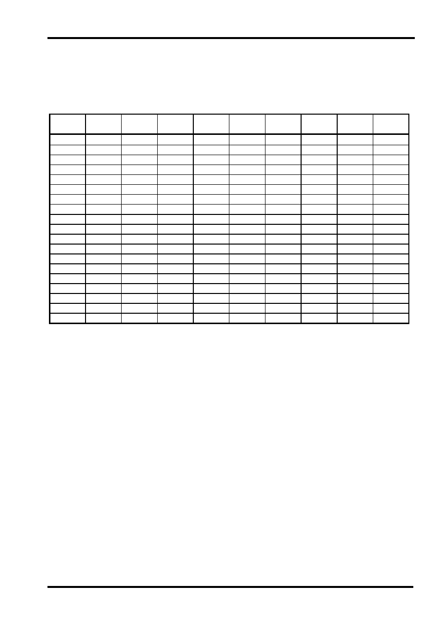
OUT V CODE OUT V CODE OUT V CODE OUT V CODE
1.5 v
15
2.5 v
25
3.5 v
35
4.5 v
45
1.6
16
2.6
26
3.6
36
4.6
46
1.7
17
2.7
27
3.7
37
4.7
47
1.8
18
2.8
28
3.8
38
4.8
48
1.9
19
2.9
29
3.9
39
4.9
49
2.0
20
3.0
30
4.0
40
5.0
50
2.1
21
3.1
31
4.1
41
2.2
22
3.2
32
4.2
42
2.3
23
3.3
33
4.3
43
2.4
24
3.4
34
4.4
44
Please contact your authorized Toko representative for voltage availability
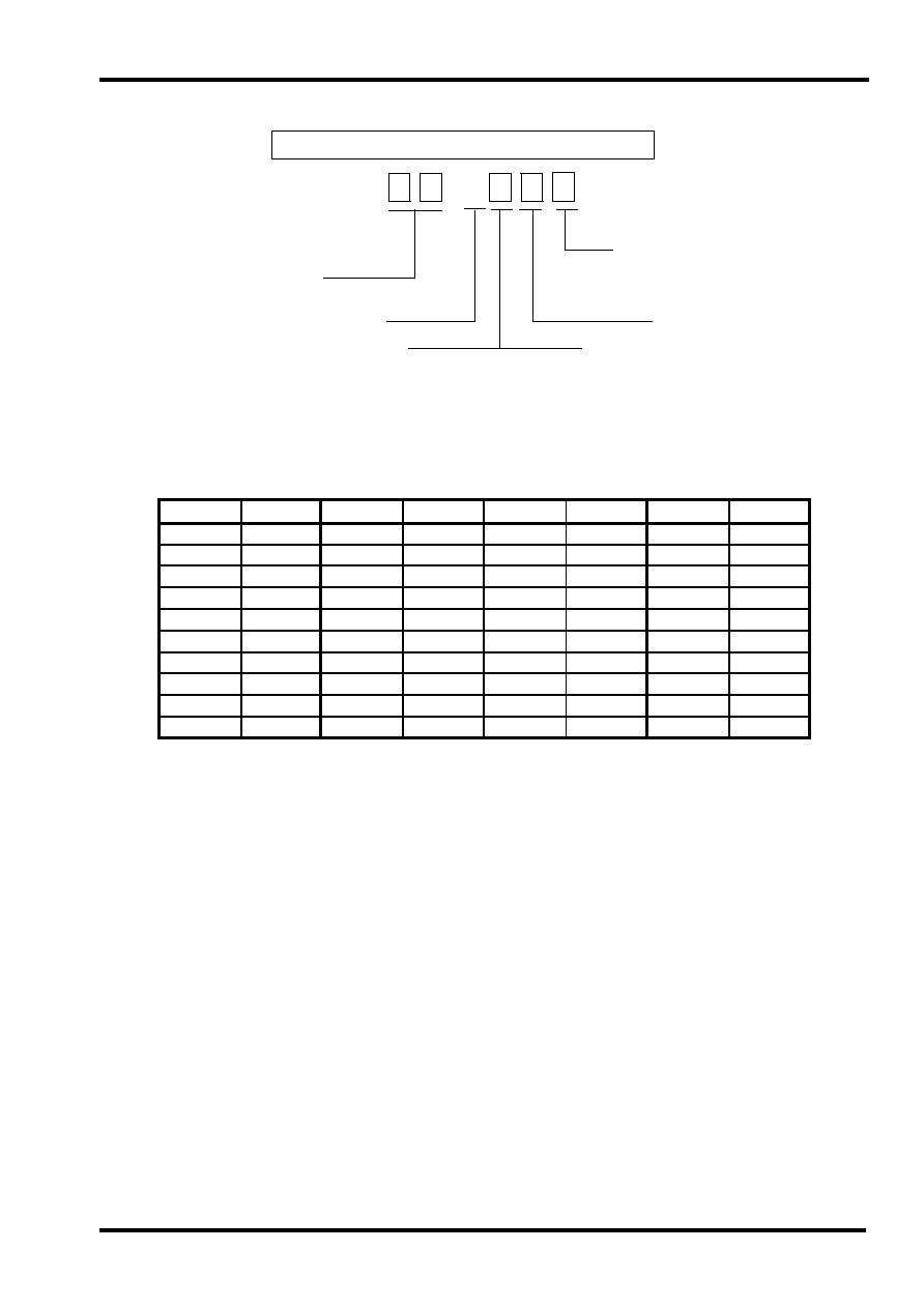
Operating Temp. Range
C:-3080
I :-4085
Voltage Code
EX 3.3V : 33
5.0V : 50
Tape/Reel Code
L:Left
Package Code
S:SOT-23
ORDERINGINFORMATION
TK
C S
(Special Sorting)
NNoise
L
TOKOInc.
IC Data Sheet
TK111xxC
GG3-H008B
Page
4
C rank device
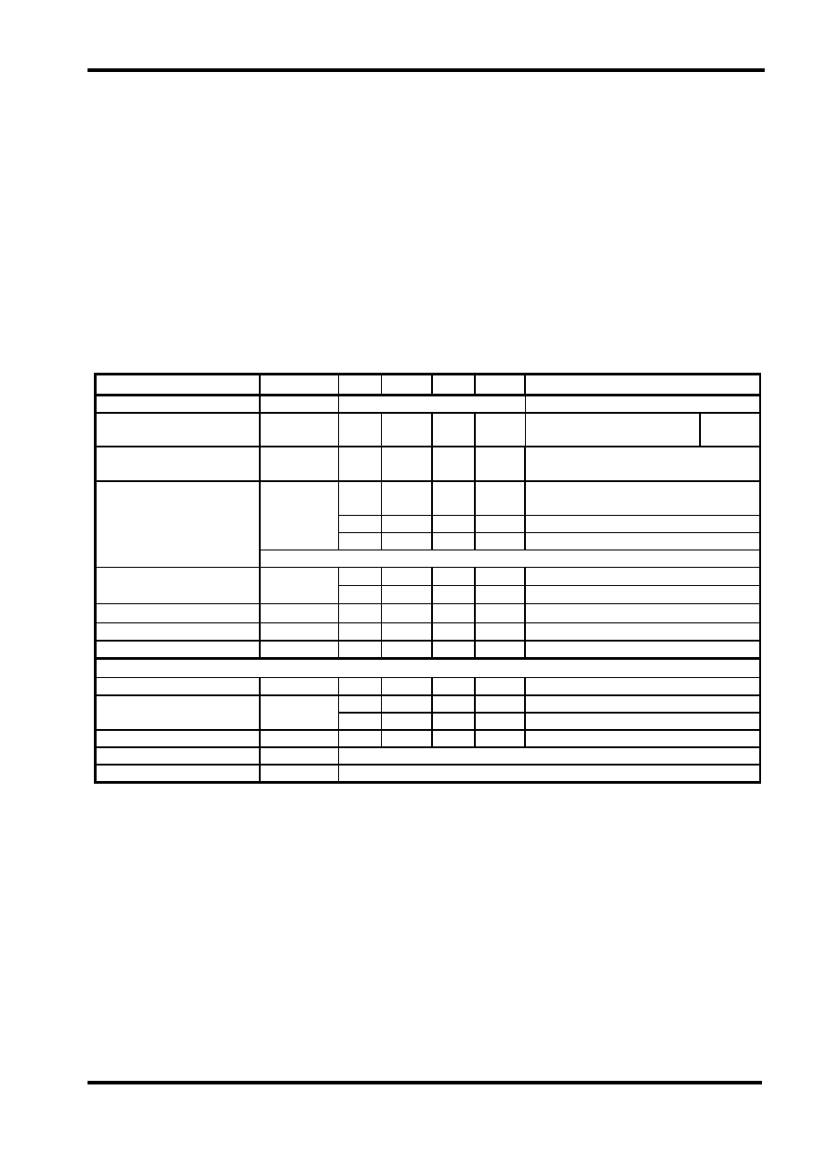
Absolute maximum ratings
Parameters
Symbol
Limiting Values
Unit
Supply voltage
cc Max
-
0.46
V
Reverse bias
VrMax
-
0.46
V
Np pin voltage
VnpMax
-
0.45
V
Control pin voltage
VcontMax
-
0.416
V
Storage temperature Range
Tstg
-
55150
Operating voltage range
Vop
1.814
Operating temperature range
Top
-3080
Short circuit current
Ishort
360
mA
Power dissipation Internal limited150mW unit
500mW mounted (reference)
5 pin mini flat package
Electrical characteristics
Test Condition
Vtest=Vout
Typ
+1V
Vcont=1.8V
Ta25
Parameters
Symbol
Min
yp Max Unit
Condition
Output voltage
Vout
See table 1
Line regulation
LinReg
0.0
5
V
Vtest=Vout
Typ
+1V---- Vout
Typ
+6V
V=5V
11 28
V
5mAIout100mA note 1
Load regulation
LoaReg
27 64
mV
5mAIout200mA note 1
80
140
mV
out=50mA
120
210
mV
out=100mA
200
350
mV
out=200mA (2.4VVout)
Vdrop
230
350
mV
out=180mA (2.1VVout2.4V)
Drop-out voltage
1.5VVout2.0VNo regulation Because of Vop
Min
=1.8V
240
320
A
When
Vout
Typ
.◊0.9
Maximum output
current
IoutMax
250
mA
1.8VVcc2.1V Reference Value
Consumption current
Icc
63
100
µ
A
out=0mA Except Icont
Standing by current
Istanby
0.0
0.1
µ
A
Vcc=8V , Vcont0.15V Off state
Quiescent current
Iq
1.0
1.8
A
Iout=50A
Control terminal Specification (Pull down resistor =500k Note 2
Control current
Icont
5
15
µ
A
Vcont1.8 on state
1.6
V
on state
Control voltage
Vcont
0.6
V
off state
Np treminal Voltage
VNp
1.28
V
Vo
Vo/Ta
Typ=35 ppm/ Reference Value
Out put noise
Vno
0.140.25
µ
V/Hz at 1KHz Reference Value
Note 1: This value depends on the output voltage. (It is a value of Vout=3V device.)
This item improves in a low voltage device.
Note 2: The input current decreases to the pA level by connecting control terminal to GND.Off state
Pull-down resistor is 500K.
General Note:
Limits are guaranteed by production testing or correction techniques using Statistical Quality Control (S
QC) methods. Unless otherwise noted. Vtest=Vout
Typ
+1vIL=1mATj=25 The operation of -30-80
is guaranteed in the design by a usual inspection.
General Note: Exceeding the "Absolute Maximum Rating " may damage the device
General Note: Connecting a capacitor to the noise bypass pin can decrease the output noise voltage
General Note: Output noise is 0.14-0.25
µ
V/Hz at 1KHz : 2565
µ
Vrms at BW400-80kHz
General Note: The ripple rejection is 84dB at 400Hz and 80dB at 1kHz.
CL=1.0
µ
F,Cnp=0.01F,Vnois=200mV
RMS
,Vin=Vout
Typ
+1.5v,Iout=10mA