 | –≠–ª–µ–∫—Ç—Ä–æ–Ω–Ω—ã–π –∫–æ–º–ø–æ–Ω–µ–Ω—Ç: TK11235 | –°–∫–∞—á–∞—Ç—å:  PDF PDF  ZIP ZIP |

IC DATA SHEET
LDO REGULATOR WITH ON/OFF SWITCH
TK112xxC
MEETING YOUR NEEDS

TOKO Inc.
IC Data Sheet
TK112xxC
GC3-H026A
Page 2
Features
∑
Very low Dropout Voltage. (Vdrop=105mV at 100mA)
∑
Very good stability (CL=0.1
µ
F is stable for any type capacitor with 2.5V
Vout)
∑
High Precision output Voltage (
±
1.5% or
±
50mV)
∑
Good ripple rejection ratio (80dB at 1KHz)
∑
Wide operating voltage range (1.8V
14.5V)
∑
Peak output current is 480mA.(10% down point)
∑
Built-in Short circuit protection
∑
Built-in Thermal Shutdown
∑
Suitable for Very Low Noise Applications
∑
Built-in on/off Control (0.1
µ
A Max Standby current) High On
∑
Very Small Surface Mount Packages SOT23L / SOT89 package
∑
Built-in reverse bias over current protection
Description
The TK112xxC is an integrated circuit with a silicon monolithic bipolar structure. The regulator is of the
low saturation voltage output type with very little quiescent current (65
µ
A).
The PNP power transistor is built-in. The I/O voltage difference is 0.17V (typical) when a current of
200mA is supplied to the system. Because of the low voltage drop, the voltage source can be effectively
used; this makes it very suitable for battery powered equipment.
The on/off function is built into the IC. The current during standby mode becomes very small (pA level).
The output voltage is available from 1.5 to 10.0V in 0.1V steps. The output voltage is trimmed with high
accuracy. This allows the optimum voltage to be selected for the equipment.
The over current sensor circuit and the reverse-bias protection circuit are built-in.
It is a very rugged design because the ESD protection is high. Therefore, the TK112xxC can be used with
confidence.
When mounted on the PCB, the power dissipation rating becomes about 600mW/ 900mW, even though
the packages are very small.
The TK112xxC features very high stability in both DC and AC.
The capacitor on the output side provides stable operation with 0.1
µ
F with 2.5V
Vout. A capacitor of
any type can be used; however, the larger this capacitor is, the better the overall characteristics are.

TOKO Inc.
IC Data Sheet
TK112xxC
GC3-H026A
Page 3
Boldface type
applies Standard Voltage.
V OUT
V CODE
V OUT
V CODE
V OUT
V CODE
V OUT
V CODE
1.5 v
15
2.5 v
25
3.5 v
35
4.5 v
45
1.6
16
2.6
26
3.6
36
4.6
46
1.7
17
2.7
27
3.7
37
4.7
47
1.8
18
2.8
28
3.8
38
4.8
48
1.9
19
2.9
29
3.9
39
4.9
49
2.0
20
3.0
30
4.0
40
5.0
50
2.1
21
3.1
31
4.1
41
2.2
22
3.2
32
4.2
42
2.3
23
3.3
33
4.3
43
2.4
24
3.4
34
4.4
44
Please contact your authorized Toko representative for voltage availability
Operating Temp. Range
C :-30
80
∞
C
I :-40
85
∞
C
Voltage Code
EX 3.3V : 33
5.0V : 50
Tape/Reel Code
L : SOT-23L
B : SOT89
Package Code
M
:
SOT23L
U
:
SOT89
ORDERING INFORMATION
T K 1 1 2
C M
(Special Sorting)
N
:
Noise
L
TOKO Inc.
IC Data Sheet
TK112xxC
GC3-H026A
Page 4
C rank device
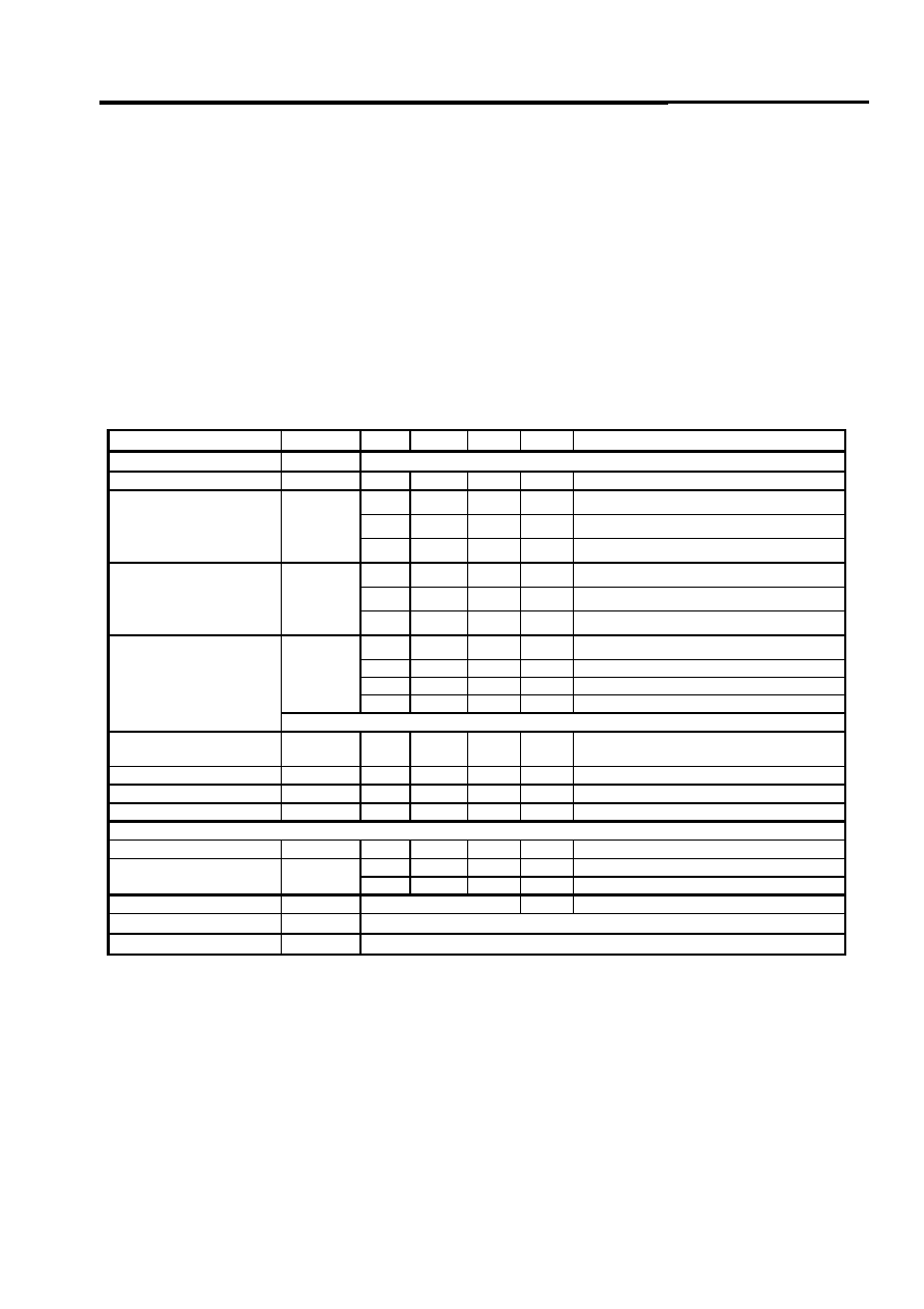
Absolute maximum ratings
Parameters
Symbol
Limiting Values
Unit
Supply voltage
Vcc Max
-
0.4
16
V
Reverse bias
VrMax
-
0.4
6
V
Np pin voltage
VnpMax
-
0.4
5
V
Control pin voltage
VcontMax
-
0.4
16
V
Storage temperature Range
Tstg
-
55
150
∞
C
Operating voltage range
Vop
1.8
14.5
V
Operating temperature range
Top
-
30
80
∞
C
Short circuit current
Ishort
500
mA
Power dissipation Internally limited
M
:
600mW mounted (reference) U
:
900mW mounted (reference)
Electrical characteristics
Test Condition Vtest=Vout
Typ
+1V
Vcont=1.8V
(Ta=25
∞
C)
Parameters
Symbol
Min
Typ
Max
Unit
Condition
Output voltage
Vout
±
1.5% or
±
50mV
Iout = 5mA
Line regulation
LinReg
0
6
mV
V=5V
Vtest=Vout
Typ
+1V---- Vout
Typ
+6V
0.5
1.1
%
5mA
<
Iout
<
100mA
1.0
2.2
%
5mA
<
Iout
<
200mA
Load regulation
2.5V
vo
5.0V
LoaReg
1.6
3.7
%
5mA
<
Iout
<
300mA
0.8
1.8
%
5mA
<
Iout
<
100mA
1.5
3.4
%
5mA
<
Iout
<
200mA
1.5V
Vo
2.4V
LoaReg
2.4
5.3
%
5mA
<
Iout
<
300mA
105
170
mV
Iout=100mA
170
270
mV
Iout=200mA
235
370
mV
Iout=300mA (2.4V
Vout)
Vdrop
235
370
mV
Iout=270mA (2.1V
Vout < 2.4V)
Dropout voltage
1.5V
Vout
2.0V
:
No regulation Because of Vop
Min
=1.8V
Maximum output
current
IoutMax
380
480
mA
(
Vout
Typ
.
◊
0.9)
Quiescent current
Iq
65
90
µ
A
Iout=0mA Excluding Icont
Standby current
Istandby
0
0.1
µ
A
Vcc=8V , Vcont
0.15V Off state
Ground pin current
Ignd
1.8
3.0
mA
Iout=100mA
Control terminal Specification
(Pull down resistor = 500k) Note 1
Control current
Icont
5
10
µ
A
Vcont=1.8V on state
1.6
V
on state
Control voltage
Vcont
0.6
V
off state
Np treminal Voltage
Vnp
1.28
V
Vo
Vo/Ta
Typ=35 ppm/
∞
C
Reference Value
Out put noise
Vno
0.14
0.25
µ
V/
Hz at1KHz Reference Value
Note 1: The input current decreases to the pA level by connecting the control terminal to GND. (Off state). The
Pull-down resistor is 500k
.
General Note: Limits are guaranteed by production testing or correction techniques using Statistical Quality
Control (SQC) methods. Unless otherwise noted. Vtest=Vout
Typ
+1V
;
IL=1mA (Tj=25
∞
C
) The
operation of
-
30
∞
C
-
80
∞
C
is guaranteed in the design by a usual inspection.
General Note: Exceeding the "Absolute Maximum Rating " may damage the device
General Note: Connecting a capacitor to the noise bypass pin can decrease the output noise voltage
General Note: Output noise is 0.14-0.25
µ
V/
Hz at 1KHz : 23
75
µ
Vrms at BW400-80kHz
General Note: The ripple rejection is 84dB at 400Hz and 80dB at 1kHz.
[CL=1.0
µ
F,Cnp=0.01
µ
F,Vnois=200mV
RMS
,Vin=Vout
Typ
+1.5v,Iout=10mA]
TOKO Inc.
IC Data Sheet
TK112xxC
GC3-H026A
Page 5
I Rank
Absolute Maximum Ratings are same as C Rank
Operating Temperature Range Top=
-
40
85
∞
C
Operating Voltage Range Vop=2.1V
14.5V
Other items are same as C rank.
Boldface type
applies over the full operating temperature range. (
-
40
85
∞
C)
Vtest=Vout
Typ
+1V Iout=5mA
Parameters
Symbol
Min
Typ
Max
Unit
Condition
Output Voltage
Vout
±
1.5% or
±
50mV
(
±
2.5% or
±
80mV)
Iout = 5mA
Line regulation
LinReg
0
6
8
mV
V=5V
0.5
1.1
1.3
%
5mA
<
Iout
<
100mA
1.0
2.2
2.8
%
5mA
<
Iout
<
200mA
Load regulation
2.5V
Vo
5.0V
LoaReg
1.6
3.7
5.3
%
5mA
<
Iout
<
300mA
0.8
1.8
2.0
%
5mA
<
Iout
<
100mA
1.5
3.4
4.1
%
5mA
<
Iout
<
200mA
1.5V
Vo
2.4V
LoaReg
2.4
5.3
6.5
%
5mA
<
Iout
<
300mA
105
170
200
mV
Iout=100mA
170
270
320
mV
Iout=200mA
Vdrop
235
370
440
mV
Iout=300mA (2.4V
Vout)
(2.2V,2.3V : No regulation)
Dropout voltage
1.5V
Vout
2.1V
:
No regulation Because of Vop
Min
=2.1V
Maximum output
current
IoutMax
380
340
480
mA
Vout= (
Vout
Typ
.
◊
0.9)
Quiescent current
Iq
65
90
100
µ
A
Iout=0mA except Icont
Standby current
Istandby
0
0.1
0.5
µ
A
Vcont
0.15V 0ff state
GND pin current
Ignd
1.8
3.0
3.6
mA
Iout=100mA
Control terminal Specification
(Pull down resistor =500k ) Note 1
Control current
Icont
5
10
12
µ
A
Vcont=1.8V on state
1.6
1.8
V
on state
Control voltage
Vcont
0. 6
0.35
V
off state
Np terminal Voltage
Vnp
1.28
V
Vo
Vo/Ta
Typ=35 ppm/
∞
C
Reference Value
Out put noise
Vno
0.14
0.25
µ
V/
Hz at1KHz Reference Value
Note 1: The input current decreases to the pA level by connecting the control terminal to GND. (Off state). The
Pull-down resistor is 500 k
.
General Note: Limits are guaranteed by production testing or correction techniques using Statistical Quality
Control (SQC) methods. Unless otherwise noted. Vtest=Vout
Typ
+1V
;
IL=1mA (Tj=25
∞
C
) The
operation of -30
∞
C
-80
∞
C
is guaranteed in the design by a usual inspection.
General Note: Exceeding the "Absolute Maximum Rating " may damage the device
General Note: Connecting a capacitor to the noise bypass pin can decrease the output noise voltage
General Note: Output noise is 0.14-0.25
µ
V/
Hz at 1KHz : 23
75
µ
Vrms at BW400-80kHz
General Note: The ripple rejection is 84dB at 400Hz and 80dB at 1kHz.
[CL=1.0
µ
F,Cnp=0.01
µ
F,Vnois=200mV
RMS
,Vin=Vout
Typ
+1.5v,Iout=10mA]
TOKO Inc.
IC Data Sheet
TK112xxC
GC3-H026A
Page 6
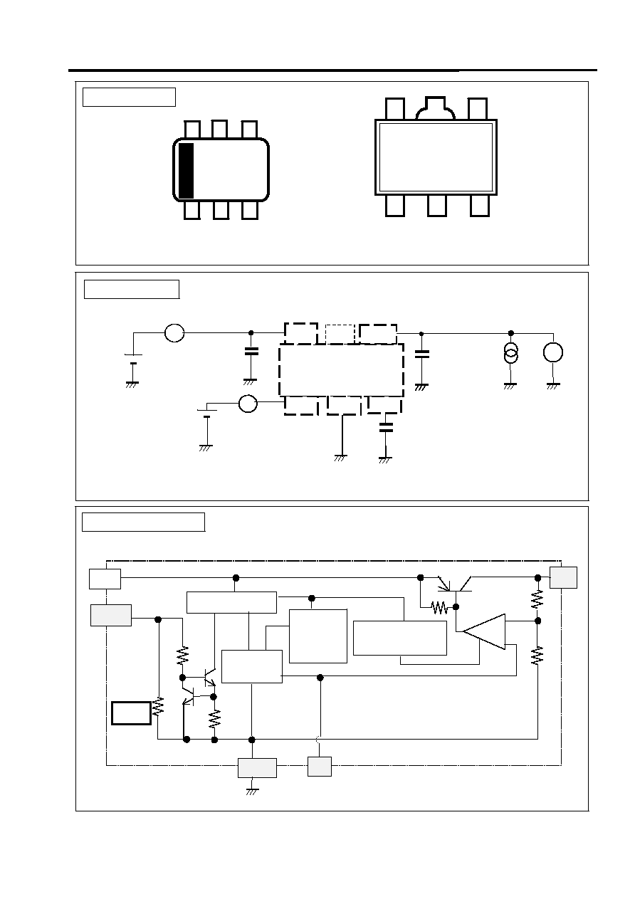
Application
Block Diagram
Pin Layout
Top view
GND
Bandgap
Reference
Cont.
Vin
Vout
Constant
Current
Source
Control Circuit
Thermal &
Over Current Protect
Np
500k
GND
Vin
1
2
3
5
4
Vout
on/off control
Np(Vref)
SOT89
Note : The terminal connection reverses between SOT-23L and SOT89.
Iin
V
CL=0.22
µ
F
(CL=1.0
µ
F)
Iout
A
Icont
Vcont
A
Cin=0.1
µ
F
Cnp=0.1
µ
F
Vin
Cont.
Vin
Vout
GND
Np
GND
Vin
1
2
3
4 Vout
On/off Control
GND
Np(Vref)
6
SOT-23L
5
GND
Terminal 2 and 5 are connected internally.
TOKO Inc.
IC Data Sheet
TK112xxC
GC3-H026A
Page 7
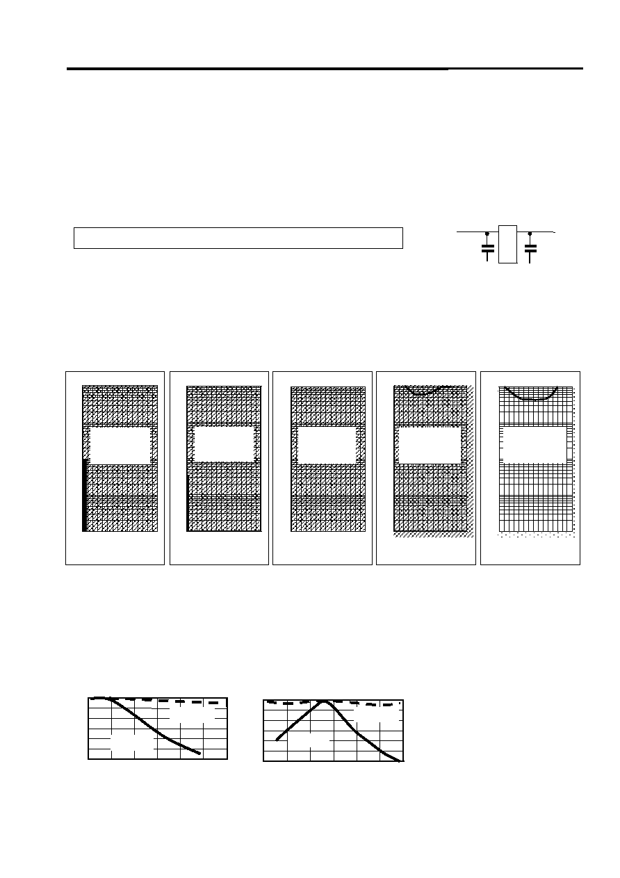
Input /Output Capacitors
Linear regulators require input and output capacitors in order to maintain the regulator's loop stability. If a 0.1
µ
F
capacitor is connected to the output side, the IC provides stable operation at any voltage in the practical current
region. However, increase the CL capacitance when using the IC in the low current region and low voltage.
Otherwise, the IC oscillates.
The equivalent series resistance (ESR) of the output capacitor must be in the stable operation area. However, it is
recommended to use as large a value of capacitance as is practical. The output noise and the ripple noise decrease
as the capacitance value increases. ESR values vary widely between ceramic and tantalum capacitors. However,
tantalum capacitors are assumed to provide more ESR damping resistance, which provides greater circuit stability.
This implies that a higher level of circuit stability can be obtained by using tantalum capacitors when compared to
ceramic capacitors with similar values.
The input capacitor is necessary when the battery is discharged, the power
supply impedance increases, or the line distance to the power supply is long.
This capacitor might be necessary on each individual IC even if two or more regulator ICs are used. It is not
possible to determine this indiscriminately. Please confirm the stability while mounted. The IC provides stable
operation with an output side capacitor of 0.1
µ
F (Vout
2.5V). If it is 0.1
µ
F or more over the full range of
temperature, either a ceramic capacitor or tantalum capacitor can be used without
considering ESR. It is not
possible to say indiscriminately. Please confirm stability while mounted.
Output voltage, Output current vs. Stable Operation Area
The above graphs show stable operation with a ceramic capacitor of 0.1uF (excluding the low current region). If the
capacitance is not increased in the low voltage, low current area, stable operation may not be achieved. Please select
the best output capacitor according to the voltage and current used. The stability of the regulator improves if a big
output side capacitor is used (the stable operation area extends.) Please use as large a capacitance as is practical.
Although operation above 150 mA has not been described, stability is equal to or better than operation at 150 mA.
Generally, a ceramic capacitor has
both a temperature characteristic and
a voltage characteristic. Please
consider both characteristics when
selecting the part. The B curves are
the recommend characteristics.
For evaluation
Kyocera
:CM05B104K10AB , CM05B224K10AB , CM105B104K16A , CM105B224K16A , CM21B225K10A
Murata
:GRM36B104K10 , GRM42B104K10 , GRM39B104K25 , GRM39B224K10 , GRM39B105K6.3
Iout [mA]
CL
0.33
µ
F All Stable
Iout [mA]
CL
0.33
µ
F All Stable
Iout [mA]
CL
0.68
µ
F All Stable
Iout [mA]
CL
1.0
µ
F All Stable
Iout [mA]
CL
2.2
µ
F All Stable
0.01
0.1
1
10
100
0.5
50
100
150
ESR[
]
Vout=5.0V
0.01
0.1
1
10
100
150
0.5
50
100
ESR [
]
Vout=4.0V
Stable Area
CL=0.068
µ
F
Vout=2.5V, 3.0V
0.01
0.1
1
10
100
0.5
50
100
150
ESR[
]
Stable Area
CL=0.068
µ
F
Vout=1.8V , 2.2V
0.01
0.1
1
10
100
2.0
50
100
150
ESR[
]
Vout=1.5V
0.01
0.1
1
10
100
4.0
50
100
150
ESR [
]
Stable Area
CL=0.1
µ
F
Stable Area
CL=0.068
µ
F
Stable Area
CL=0.068
µ
F
The recommended value : Cin=CL=0.22
µ
F(MLCC) Iout
0.5mA.
Cin=0.22
µ
F
0.1
µ
F
Vout
CL=0.22
µ
F
0.1
µ
F
%
Capacitance vs. Voltage
0
Bias voltage(V)
CAP
2
4
6
8
10
50
60
70
80
90
100
B Curve
F Curve
Capacitance vs. Temperature
%
60
50
80
90
100
70
CAP
-50 -25
0
25
50
75 100
Ta(
∞
C)
B Curve
F Curve

TOKO Inc.
IC Data Sheet
TK112xxC
GC3-H026A
Page 8
Output noise
Increase Cnp to decrease the noise. The recommended Cnp capacitance is 6800pF(682) ~ 0.22
µ
F(224).
The amount of noise increases with the higher output voltages.
TK11230C Cnp vs. Noise
Iout=30mA BPF=400Hz
80kHz
TK11230CM Cin=10
µ
F Iout=10mA
TK11230C Cnp vs Noise
CnpF
Noise
µ
Vrms)
0
50
100
150
200
250
300
1
10
100
1000
10000
100000
CL=0.22
µ
F
CL=0.47
µ
F
CL=1.0
µ
F
CL=2.2
µ
F
CL=10
µ
F
Iout=30mA BPF:400
80kHz
CL=Tantal
CL=MLCC
TK11230C Iout vs Noise
35
40
45
50
55
60
65
70
75
80
85
90
95
0
50
100
150
200
250
300
Iout(mA)
Noise(
µ
Vrms)
Cnp=10000pF BPF:400
80kHz
CL=Tantal
CL=0.22uF
CL=0.47uF
CL=1.0uF
CL=2.2uF
CL=10uF
TK11230C Iout vs. Noise
35
40
45
50
55
60
65
70
75
80
85
90
95
0
50
100
150
200
250
300
Iout(mA)
Noise(
µ
Vrms)
Cnp=10000pF BPF:400
80kHz
CL=MLCC
CL=0.22uF
CL=0.47uF
CL=1.0uF
CL=2.2uF
CL=10uF
Noise Level(1/f)
0.01
0.1
1
10
10
100
1k
10k
100k
Frequency
Hz)
Noise(
µ
V/
Hz)
CL=0.22
µ
FCeramic)
Cnp=0.01
µ
F
Cnp=0.1
µ
F
Cnp=1000pF
Noise
(
µ
Vrms)
TK112xxC Vout vs Noise
10
20
30
40
50
60
70
80
90
1.0 1.5 2.0 2.5 3.0 3.5 4.0 4.5 5.0
Vout(V)
Iout=30mA Cnp=10000pF CL=0.22
µ
F(MLCC)
BPF:400
80kHz
TOKO Inc.
IC Data Sheet
TK112xxC
GC3-H026A
Page 9
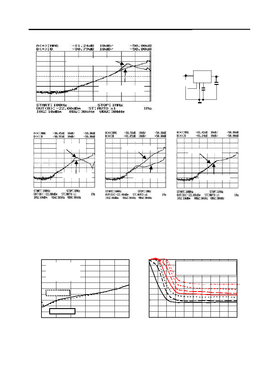
Ripple rejection
The ripple rejection characteristic depends on the characteristic and the capacitance value of the capacitor
connected to the output side. The RR characteristic of 50KHz or more varies greatly with the capacitor on the
output side and PCB pattern. If necessary, please confirm stability while operating.
CL
GND
112XX
Vout
Vin
Cnp
0.1
µ
F
Vcont
CL=1 uF (Tantal)
CL=1uF (MLCC)
CL=0.22uF (MLCC)
CL=0.22 uF (Tantal)
A : Cref=0.1uF
B : Cref=0.001uF
Ripple Rejection vs. Iout
-100
-90
-80
-70
-60
-50
-40
-30
-20
-10
0
0
50
100
150
200
250
300
Iout(mA)
R.R(dB)
Cnp=0.01
µ
F
CL=0.22
µ
FCeramic)
Vin=5.0V
Vripple=500mVp-p
Freq=1kHz
Freq=400Hz
Ripple Rejection at Low Vin
-100
-90
-80
-70
-60
-50
-40
-30
-20
-10
0
0 0.1 0.2 0.3 0.4 0.5 0.6 0.7 0.8 0.9 1.0
Vin-Vout_Typ(V)
R.R (dB)
Cin:None
Vripple=100mVp-p
Freq:1kHz
Cnp:0.01
µ
F CL:0.22
µ
F (Ceramic)
Vin=5.0V Vout=3.0V Iout=10mA
VR=500mVp-p f=100
1MHz Cnp=0.1uF
A : CL=10uF ( Tantal)
B : CL=0.22uF ( Tantal)

TOKO Inc.
IC Data Sheet
TK112xxC
GC3-H026A
Page 10
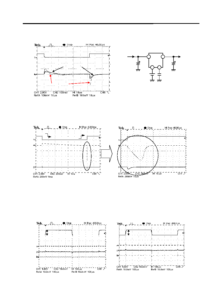
TK112xxCM Transient
∑
ON / OFF Transient
112xxC
Cnp
CL
Iout=30mA
Cin
1
µ
F
Vin
=Vout
TYP
+1V
1
3
6
4
Vcont=0V
2V
(f=100Hz)
CL= Variable Cnp=0.001
µ
F
CL= Variable Cnp=0.01
µ
F
Cnp= Variable CL=1
µ
F
CL= Variable Cnp=0.01
µ
F Io=30mA
The rise time of the regulator depends on CL and Cnp; the fall time depends on CL.
1.0V/div
250
µ
s/div
Vou
t
Vcont
OFF
ON
Cnp=
0.001
µ
F
0.1
µ
F
0.01
µ
F
1.0V/div
10
µ
s/div
Vou
t
Vcont
OFF
ON
CL=
0.22
µ
F
2.2
µ
F
1.0
µ
F
1.0
µ
F ,
2.2
µ
F
1.0V/div
50
µ
s/div
Vou
t
Vcont
OFF
ON
CL=
0.22
µ
F
1.0V/div
250
µ
s/div
Vou
t
Vcont
OFF
ON
1.0
µ
F
2.2
µ
F
CL=
0.22
µ
F
TOKO Inc.
IC Data Sheet
TK112xxC
GC3-H026A
Page 11
∑
LOAD Transient
112xxC
Cnp
CL
Cin
1
µ
F
Vcont
1.8V
Vin
=Vout
TYP
+1V
1
3
6
4
Iout
ON
OFF
0.01
µ
F
When the capacitor on the load side is increased, the load change becomes smaller.
The no load voltage change can be greatly improved by delivering a little
load current to ground (see right curve above).
Increase the load side capacitor when the load change is fast or when there is a large current change. In addition, at
no load, the voltage change can be reduced by delivering a little load current to ground.
∑
Line Transient
Vout
Iout
3mA
33mA
3mA
33mA
CL=1.0
µ
F
2.2
µ
F
CL=0.22
µ
F
CL= Variable Cnp=0.01
µ
F
Vout
Vin
1V
CL=0.22
µ
F
CL=1.0
µ
F
CL=2.2
µ
F
CL= Variable Cnp=0.01
µ
F
Vout
Vin
1V
Cnp=0.001
µ
F
Cnp=0.01
µ
F
Cnp=0.1
µ
F
Cnp= Variable CL=1
µ
F
Vout
Iout
33mA 30mA
3mA 0mA
30mA 33mA
0mA 3mA
Iout=0
30mA
Iout=3
33mA
Iout=0
30mA , 3
33mA
Vout
Iout
Iout=0
30mA
Iout=3
33mA
Magnification

TOKO Inc.
IC Data Sheet
TK112xxC
GC3-H026A
Page 12
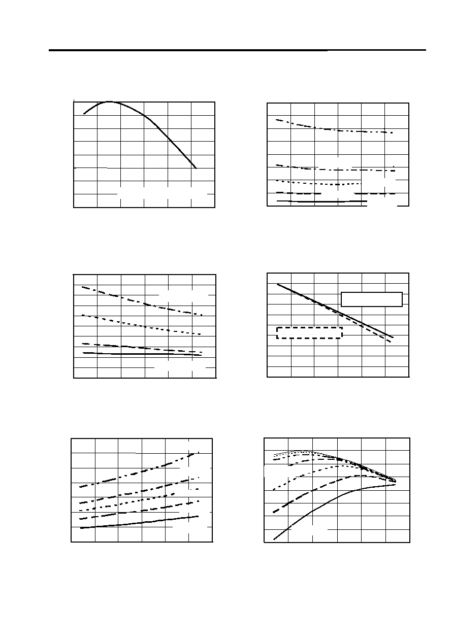
Load regulation
0
50
100
150
200
250
300
Iout(mA)
Vout(mV)
Vo=3.0V
-80
-70
-60
-50
-40
-30
-10
0
10
-20
Vo=2.0V
Vo=5.0V
-35
-30
-25
-20
-15
-10
-5
0
5
10
15
0
5
10
15
20
Vin(V)
Vout(mV)
Vo1.5V
Vo2.0V
Vo3.0V
Vo4.0V
Vo5.0V
Line regulation
Vdrop
-500
-450
-400
-350
-300
-250
-200
-150
-100
-50
0
0
100
200
300
400
500
Iout(mA)
Vdrop(mV)
Regulation point
100
Vin(mV)
-300
-200
-100
0.0
100
Vout(mV)
Iout=300mA
Iout=0mA
Iout=0mA,50mA,100mA,150mA,200mA,250mA,300mA
Vcont vs. Icont
0
5
10
15
20
0.0
1.0
2.0
3.0
4.0
5.0
Vcont(V)
Icont(
µ
A)
Icont
Vout

TOKO Inc.
IC Data Sheet
TK112xxC
GC3-H026A
Page 13
Standby current
1.E-12
1.E-11
1.E-10
1.E-09
1.E-08
1.E-07
1.E-06
1.E-05
1.E-04
0
2
4
6
8 10 12 14 16 18 20
Vin(V)
Istandby(A)
Short circuit current
0.0
1.0
2.0
3.0
4.0
5.0
6.0
0
100
200
300
400
500
Iout(mA)
Vout(V)
GND current
0
1
2
3
4
5
6
7
8
9
10
11
12
0
50
100
150
200
250
300
Iout(mA)
Ignd(mA)
Vo1.5V
Vo2.0V
Vo3.0V
Vo4.0V
Vo5.0V
Reverse bias current
0
10
20
30
40
50
60
0 1 2 3 4 5 6 7 8 9 10
Vrev(V)
Irev(
µ
A)
Vout=5V
Vout=2V
Vout=4V
Vout=3V
IoutMax(mA)
IoutMax at low Vop
TK11215
TK11224
0
50
100
150
200
250
300
350
400
450
500
1.7
1.8
1.9
2.0
2.1
2.2
2.3
2.4
VopV)
TOKO Inc.
IC Data Sheet
TK112xxC
GC3-H026A
Page 14
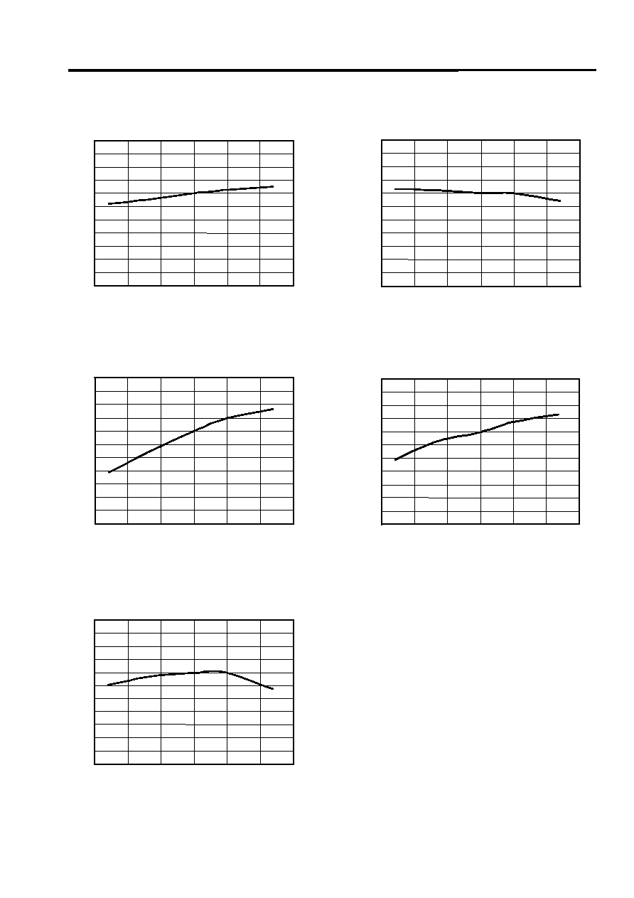
Temperature Characteristics
(Ta: Ambient temperature)
Iout (mA)
Max Iout
340
360
380
400
420
440
460
480
500
-50
-25
0
25
50
75
100
Ta(
∞
C)
Vout=(Vout
Typ
.
◊
0.9
GND current
Ignd(mA)
Iout=300mA
0.0
2.0
4.0
6.0
8.0
10.0
12.0
14.0
16.0
-50
-25
0
25
50
75
100
Ta(
∞
C)
Io=50mA
Io=100mA
Io=150mA
Io=200mA
on/off point
Vcont(V)
0.6
0.7
0.8
0.9
1.0
1.1
1.2
1.3
1.4
1.5
1.6
-50
-25
0
25
50
75
100
Ta(
∞
C)
Vcont(ONpoint)
Vcont(OFFpoint)
Control current
Icont(
µ
A)
0.0
2.0
4.0
6.0
8.0
10.0
12.0
14.0
16.0
18.0
20.0
-50
-25
0
25
50
75
100
Ta(
∞
C)
Vcont=1.8V
Vcont=4.0V
Vcont=2.0V
Vcont=3.0V
Dropout voltae
Vdrop(mV)
-50
-25
0
25
50
75
100
Ta(
∞
C)
0
50
100
150
200
250
300
350
Io=300mA
Io=100mA
Io=150mA
Io=200mA
Io=50mA
150
200
250
300
350
400
450
500
550
-50
-25
0
25
50
75
100
Ta(
∞
C)
IoutMAX(mA)
Vin=1.9/2.0/2.1/2.2/2.3/2.4/2.5V
Output current
Vin=1.9V
Vin=2.2V
Vin=2.0V
Vin=2.1V
TOKO Inc.
IC Data Sheet
TK112xxC
GC3-H026A
Page 15
Output voltage vs. Temperature characteristics
-35
-30
-25
-20
-15
-10
-5
0
5
10
15
20
-50
-25
0
25
50
75
100
Ta()
Vout(mV)
Vout=3.0V
-35
-30
-25
-20
-15
-10
-5
0
5
10
15
20
-50
-25
0
25
50
75
100
Ta(
∞
C)
Vout(mV)
Vout=2.0V
-35
-30
-25
-20
-15
-10
-5
0
5
10
15
20
Vout(mV)
Vout=4.0V
-50
-25
0
25
50
75
100
Ta()
Vout(mV)
Vout=1.5V
-50
-25
0
25
50
75
100
Ta(
∞
C)
-35
-30
-25
-20
-15
-10
-5
0
5
10
15
20
Vout(mV),
Vout=5.0V
-50
-25
0
25
50
75
100
Ta()
-35
-30
-25
-20
-15
-10
-5
0
5
10
15
20

TOKO Inc.
IC Data Sheet
TK112xxC
GC3-H026A
Page 16
Layout
PCB Material : Glass epoxy t=0.8mm
SOT23L-6
SOT89-5
Derating Curve
The package loss is limited at the temperature that the internal temperature sensor works (about 150
∞
C).
Therefore, the package loss is assumed to be an internal limitation. There is no heat radiation
characteristic of the package unit assumed because of the small size. Heat is carried away by the device
being installed on the PCB. This value changes by the material and the copper pattern etc. of the PCB.
The losses are approximately 600mW (SOT-23L) : 900mW(SOT-89). Enduring these losses becomes
possible in a lot of applications operating at 25
∞
C.
Determining the thermal resistance when mounted on a PCB.
The operating chip junction temperature is shown by
Tj=
ja
◊
Pd + Ta. Tj of the IC is set to about 150
∞
C.
Pd is a value when the overtemperature sensor is made to work.
Pd is easily obtained.
Mount the IC on the print circuit board. Short between the output pin and ground. after that, raise input
voltage from 0V to evaluated voltage (see*1) gradually.
At shorted the output pin, the power dissipation P
D
can be expressed as Pd=Vin
◊
Iin.
The input current decreases gradually as the temperature of the chip becomes high. After a while, it
reaches the thermal equilibrium. Use this currrent value at the thermal equilibrium. In almost all the
cases, it shows 600mW(SOT23L-6)900mW(SOT89-5) or more.
*1 In the case that the power, Vin
◊
Ishort(Short Circuit Current), becomes more than twice of the maximum rating of its power
dissipation in a moment, there is a possibility that the IC is destroyed before internal thermal protection works.
Pd is obtained by the normal temperature in degrees. The current that can be used at the highest
operating temperature is obtained from the graph of the figure below.
Procedure (Do when PCB mounted).
1. Pd is obtained (Vin
◊
Iin when the output side is short-circuited).
2. Pd is plotted on the horizontal line to 25
∞
C.
3. Pd is connected with the point of 150
∞
C by the straight line
(bold face line).
4. A line is extended vertically above the point of use temperature in the
design. For instance, 75
∞
C is assumed (broken line).
5. Extend the intersection of the derating curve (fat solid line) and (broken
line) to the left and read the Pd value.
6. DPd
˜
(Vinmax
-
Vout)=Iout (at 75
∞
C)
The maximum current that can be used at the highest operating temperature is:
Iout
DPd
˜
(Vinmax
-
Vout).
Please do derating with 4mW/
∞
C at
Pd=600mW and 25
∞
C or more. Thermal
resistance is (
ja=250
∞
C / W).
Vout
On/off
Vin
Please do derating with 7.2mW/
∞
C at
Pd=900mW and 25
∞
C or more.
Thermal resistance is (
ja=138
∞
C / W)
600
SOT-89
-7.2mW/
∞
C
25
50
∞
C
100
150
0
Pd(mW)
(85)
∞
C
900
SOT-23- L
-4.8mW/
∞
C
0
on/off
Vin
Vout
Ta (Ta=25
∞
C)
150 =
ja
◊
pd + 25
ja
◊
Pd = 125
ja = (125/ pd) (
∞
C / mW)
Pd(mW)
25 50
100
150
∞
C
0
(75)
DPd
Pd
2
3
4
5

TOKO Inc.
IC Data Sheet
TK112xxC
GC3-H026A
Page 17
Application hint
On/Off Control
It is recommended to turn the regulator Off when the
circuit following the regulator is non-operating. A design
with little electric power loss can be implemented. We
recommend the use of the on/off control of the regulator
without using a high side switch to provide an output from
the regulator. A highly accurate output voltage with low
voltage drop is obtained.
Because the control current is small, it is possible to control it directly by CMOS logic.
The PULLDOWN resistance (500K
) is built into the control terminal.
The noise and the ripple rejection characteristics depend on the capacitance on the Vref terminal.
The ripple rejection characteristic of the low frequency region improves by increasing the
capacitance of Cnp.
A standard value is Cnp=0.068
µ
F. Increase Cnp in a design with important output noise and ripple
rejection requirements. The IC will not be damaged if the capacitor value is increased.
The on/off switching speed changes depending on the Np terminal capacitance. The switching speed
slows when the capacitance is large.
Parallel connected ON/OFF Control
Current boost
For current boost applications, use the products below. A low voltage drop, high current regulator
can be easily made.
TK714xx Only the PNP transistor for the current boost is external.
TK732xx ( For Iout=10A Max regulator)
Built-in Short circuit protection: a constant current can be set by an external
resistor.
The figure at the left illustrates multiple regulators being
controlled by a single On/Off control signal. There is a
possibility of overheating because the power loss of the low
voltage side IC (TK11220C) is large. The series resistor
(R) is put in the input line of the low output voltage
regulator in order to prevent over-dissipation. The voltage
dropped across the resistor reduces the large input-to-
output voltage across the regulator, reducing the power
dissipation in the device. When the thermal sensor works,
a decrease of the output voltage, oscillation, etc. may
be observed.
2.0V
5V
3.3V
On/Off Cont.
Vin
TK11250C
TK11233C
TK11220C
R
REG
Vsat
OP
On/Off Cont.

TOKO Inc.
IC Data Sheet
TK112xxC
GC3-H026A
Page 18
Definition of Term s
The output voltage tables are specified with a test voltage of Vin=Output Voltage (Typ.) + 1V.
Output Voltage ( Vout )
The output voltage is specified with (Vin = Output Voltage (Typ.) + 1V) and output current
(Iout=5mA).
Maximum Output Current ( Iout Max )
The output current is measured when the output voltage decreases to
(
Vout
Typ
. x 0.9)
. The input
voltage is (Output Voltage (Typ.) + 1V). The maximum output current is measured in a short
time so that it is not influenced by the temperature of the chip. The output current decreases
with low voltage operation.
Please refer to the "Low input voltage-output current" graph for 2.1V or less.
Dropout Voltage ( Vdrop )
The dropout voltage is the difference between the input voltage and the output voltage at which
point the regulator starts to fall out of regulation. Below this value, the output voltage will fall
as the input voltage is reduced. It is dependent upon the load current (Iout) and the junction
temperature (Tj). The input voltage is gradually decreased below the test voltage. It is the
voltage difference between the input and the output when the output voltage decreases by
100mV.
Line Regulation ( Lin Reg )
Line regulation is the ability of the regulator to maintain a constant output voltage as the input
voltage changes. The line regulation is specified as the input voltage is changed from (Output
Voltage (Typ.) + 1V) to (Output Voltage (Typ.) + 6V). This measurement is not influenced by the
temperature of the IC and is measured in a short time.
Load Regulation ( Load Reg )
Load regulation is the ability of the regulator to maintain a constant output voltage as the load
current changes. The input voltage is set to (Output Voltage (Typ.) + 1V). The output voltage
change is measured as the load current changes from to 5 to 100mA and from 5 to 200mA. This
measurement is not influenced by the temperature of the IC and is measured in a short time.
Quiescent Current ( Iq )
The quiescent current is the current which flows through the ground terminal under no load
conditions (Io=0mA).
Ripple Rejection ( RR )
Ripple rejection is the ability of the regulator to attenuate the ripple content of the input voltage
at the output. It is specified with the input voltage = ( Vout + 1.5V ) , Iout=10mA, CL=1.0
µ
F
and C
np
=0.01
µ
F
An Alternating Current source of (f=1KHz and 200mV
RMS
) is superimposed to
the power-supply voltage. Ripple rejection is the ratio of the ripple content of the output vs. the
input and is expressed in dB. It is typically about 80dB at 1KHz. The ripple rejection improves
when the value of the capacitor at the noise bypass terminal in the circuit is large. However,
the on/off response worsens.
Standby Current .( Istandby )
Standby current is the current which flows into the regulator when the control voltage is made 0
volts. It is measured with an input voltage of 8V.
TOKO Inc.
IC Data Sheet
TK112xxC
GC3-H026A
Page 19
PROTECTION CIRCUIT S
Thermal Sensor
The thermal sensor protects the device if the junction temperature exceeds the safe value (Tj=150
∞
C). This temperature rise can be caused by extreme heat, excessive power dissipation caused by
large output voltage drops, or excessive output current. The regulator will shut off when the
temperature exceeds the safe value. As the junction temperature decreases, the regulator will
begin to operate again. Under sustained fault conditions, the regulator output will oscillate as the
device turns off then resets. Please improve heat radiation or lower the input electric power. When
heat radiation is poor, the forecast package loss is not obtained.
* In the case that the power, Vin
◊
Ishort(Short Circuit Current), becomes more than twice of the maximum rating of its power
dissipation in a moment, there is a possibility that the IC is destroyed before internal thermal protection works.
Reverse Bias Current
The reverse bias protection prevents excessive current from flowing
through the IC even if the input voltage becomes 0 with
voltage impressed on the output side (input short-circuited to
GND). The maximum reverse bias voltage is 6V.
∑
ESD .......... MM 200pF 0
200V Min
HBM 100pF 1.5k
2000V Min
Vout
Vin
GND

TOKO Inc.
IC Data Sheet
TK112xxC
GC3-H026A
Page 20
Outline ;
PCB ;
Stamps
SOT23L-6
V OUT V CODE V OUT V CODE V OUT V CODE
V OUT V CODE
1.5 v
15
2.5 v
25
3.5 v
35
4.5 v
45
1.6
16
2.6
26
3.6
36
4.6
46
1.7
17
2.7
27
3.7
37
4.7
47
1.8
18
2.8
28
3.8
38
4.8
48
1.9
19
2.9
29
3.9
39
4.9
49
2.0
20
3.0
30
4.0
40
5.0
50
2.1
21
3.1
31
4.1
41
2.2
22
3.2
32
4.2
42
2.3
23
3.3
33
4.3
43
2.4
24
3.4
34
4.4
44
The output voltage table indicates the standard value when manufactured.
Please contact your authorized Toko representative for voltage availability
Voltage
Code
M
M
R X X
0.4
+0.15
-
0.05
0.1
5
-
0.32
+0.15
-
0.05
0.1
0.95
0.95
TypeCode
e
e
Recommended Mount Pad
0.95
0.95
1.0
0.6
3.0
e
e
e
1
1.4Max
2.2
±
0.2
0.15
±
0.1
0
0.1
1.2
±
0.2
0.3
3.3
±
0.3
0.4
±
0.2
15∫Max
+0.3
-
0.1
(3.4)
3.5
0.1
Molded Resin with Body : Epoxy Resin
Lead Frame
: Copper Alloy
Treatment
: Solder Plating(5
15
µ
m)
Marking Method
: Ink or Laser
Weight
: 0.023g
Country of origin
:Japan or Korea
Unit : mm
General tolerance :
±
0.2

TOKO Inc.
IC Data Sheet
TK112xxC
GC3-H026A
Page 21
SOT89-5
V OUT V CODE V OUT V CODE V OUT V CODE
V OUT V CODE
1.5 v
15
2.5 v
25
3.5 v
35
4.5 v
45
1.6
16
2.6
26
3.6
36
4.6
46
1.7
17
2.7
27
3.7
37
4.7
47
1.8
18
2.8
28
3.8
38
4.8
48
1.9
19
2.9
29
3.9
39
4.9
49
2.0
20
3.0
30
4.0
40
5.0
50
2.1
21
3.1
31
4.1
41
2.2
22
3.2
32
4.2
42
2.3
23
3.3
33
4.3
43
2.4
24
3.4
34
4.4
44
The output voltage table indicates the standard value when manufactured.
Please contact your authorized Toko representative for voltage availability
Unit : mm
General tolerance :
±
0.2
Molded Resin with Body : Epoxy Resin
Lead Frame
: Copper Alloy
Treatment
: Solder Plating(5
15
µ
m)
Marking Method
: Ink or Laser
Weight
: 0.053 g
Country of origin
: Japan
1.0
1.0
2.5
±
0.2
4.5
+0.5
-
0.3
0.44
Max
VOLTAGE
CODE
0.49
Max
0.49
Max
0.49
Max
1.6
4.5
±
0.2
0.49
Max
0.49
Max
0.54
Max
1.0
2.5
±
0.2
0.4
X
X
LOT No
TYPE CODE
R:112XX
0.7Max
1.0
0.7Max
1.5
1.5
2.0
1.5
0.7
0.8
1.5
0.7
45∞
Recommended Mount Pad
e
e
1.5
±
0.2
1.5
1.5
3.0
e
e
e'

TOKO Inc.
IC Data Sheet
TK112xxC
GC3-H026A
Page 22
NOTE
Please be sure that you carefully discuss your planned purchase with our office if you intend to use the
products in this data sheet under conditions where particularly extreme standards of reliability are
required, or if you intend to use products for applications other than those listed in this data sheet.
l Power drive products for automobile, ship or aircraft transport systems; steering and navigation
systems, emergency signal communications systems, and any system other than those mentioned
above which include electronic sensors, measuring, or display devices, and which could cause major
damage to life, limb or property if misused or failure to function.
l Medical devices for measuring blood pressure, pulse, etc., treatment units such as coronary
pacemakers and heat treatment units, and devices such as artificial organs and artificial limb systems
which augment physiological functions.
l Electrical instruments, equipment or systems used in disaster or crime prevention.
n Semiconductors, by nature, may fail or malfunction in spite of our devotion to improve product quality
and reliability. We urge you to take every possible precaution against physical injuries, fire or other
damages which may cause failure of our semiconductor products by taking appropriate measures,
including a reasonable safety margin, malfunction preventive practices and fire-proofing when
designing your products.
n This data sheet is effective from
Oct. 2002
. Note that the contents are subject to change or
discontinuation without notice. When placing orders, please confirm specifications and delivery
condition in writing.
n TOKO is not responsible for any problems nor for any infringement of third party patents or any other
intellectual property rights that may arise from the use or method of use of the products listed in this
data sheet. Moreover, this data sheet does not signify that TOKO agrees implicitly or explicitly to
license any patent rights or other intellectual property rights which it holds.
n None of ozone depleting substances(ODS) under the Montreal Protocol is used in manufacturing
process of us.
If you need more information on this product and other TOKO products, please contact us.
OFFICE
n TOKO Inc. Headquarters
1-17, Higashi-yukigaya 2-chome, Ohta-ku, Tokyo,145-8585, Japan
TEL: +81.3.3727.1161
FAX: +81.3.3727.1176 or +81.3.3727.1169
Web site:
http://www.toko.co.jp/
n TOKO America
Web site:
http://www.toko.com/
n TOKO Europe
Web site:
http://www.tokoeurope.com/
n TOKO Hong Kong
Web site:
http://www.toko.com.hk/
n TOKO Taiwan
Web site:
http://www.tokohc.com.tw/
n TOKO Singapore
Web site:
http://www.toko.com.sg/
n TOKO Seoul
Web site:
http://www.toko.co.kr/
n TOKO Manila
Web site:
http://www.toko.com.ph/
n TOKO Brazil
Web site:
http://www.toko.com.br/
YOUR DISTRIBUTOR
MEETING YOUR NEEDS
TO BUILD THE QUALITY RELIED BY COSTOMERS