TK112xx
January, 1996 TOKO, Inc.
Page 1
1-3-96
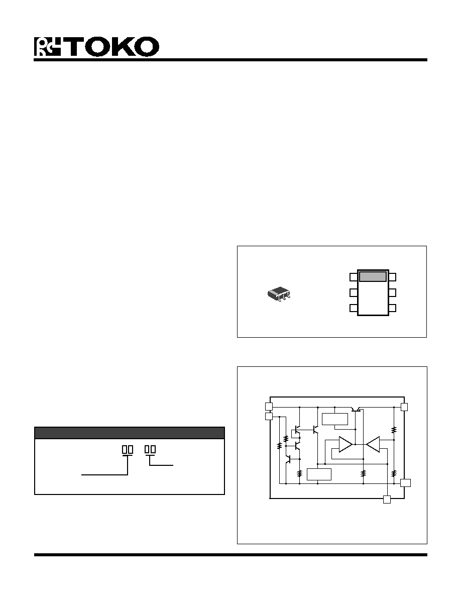
TK112XXM
BLOCK DIAGRAM
VOLTAGE REGULATOR WITH ON/OFF SWITCH
FEATURES
s
Low Dropout Voltage
s
CMOS/TTL Compatible ON/OFF Switch
s
Very Low Standby Current 180
µ
A (ON, No Load)
s
Internal Thermal Shutdown
s
Short Circuit Protection
s
Very Low (0.1
µ
A) Current in OFF Mode
s
Low Noise with External Bypass Capacitor
APPLICATIONS
s
Battery Powered Systems
s
Cellular Telephones
s
Pagers
s
Personal Communications Equipment
s
Portable Instrumentation
s
Portable Consumer Equipment
s
Radio Control Systems
s
Toys
s
Low Voltage Systems
1
3
CONTROL
GND
6
4
V
IN
V
O
TK112
M PO
2
5
GND
BYPASS
DESCRIPTION
The TK112XX is a low power, linear regulator with a built-
in electronic switch. The internal electronic switch can be
controlled by TTL or CMOS logic levels. The device is in
the ON state when the control pin is pulled to a high logic
level. A pin for a bypass capacitor is provided, which
connects to the internal circuitry, to lower the overall output
noise level.
An internal PNP pass-transistor is used in order to achieve
low dropout voltage (typically 100 mV at 30 mA load
current). The device has very low quiescent current (180
µ
A) in the ON mode with no load and 1 mA with 30 mA load.
The quiescent current is typically 2.5 mA at 60 mA load.
When the device is in standby mode (V
CONT
= 0), the
quiescent current is typically 100 nA. An internal thermal
shutdown circuit limits the junction temperature to below
150
∞
C. The load current is internally monitored and the
device will shut down in the presence of a short circuit at the
output.
TK112
M
Voltage Code
Tape/Reel Code
TAPE/REEL CODE
BX : Bulk/Bag
TL : Tape Left
ORDERING INFORMATION
VOLTAGE CODE
27 = 2.75 V
30 = 3.0 V
32 = 3.25 V
35 = 3.5 V
40 = 4.0 V
45 = 4.5 V
47 = 4.75 V
50 = 5.0 V
S
S
S
S
S
S
S
S
S
S
S
V
O
GND
TK112xx
+
≠
BANDGAP
REFERENCE
THERMAL
PROTECTION
≠
+
S
NOISE
BYPASS
S
S
S
S
S
S
V
IN
CONTROL
S
S
3
2,5
4
6
1
P50
Page 2
1-3-96
TK112xx
January, 1996 TOKO, Inc.
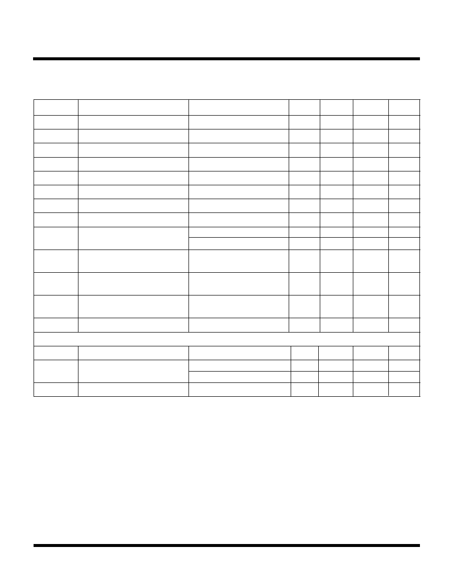
SYMBOL
PARAMETER
TEST CONDITIONS
MIN
TYP
MAX
UNITS
V
IN
Supply Voltage Range
1.8
15
V
I
IN
Supply Current
I
O
= 0 mA, Except I
CONT
170
350
µ
A
I
INS
Standby Current
V
IN
= 8 V, Output off
0.1
µ
A
V
O
Output Voltage
I
O
= 30 mA
2.66
2.75
2.84
V
V
DROP
Dropout Voltage
I
O
= 60 mA
0.18
0.3
V
I
O
Output Current
Note 3
150
170
mA
I
OR
Recommended Output Current
130
mA
Line Reg
Line Regulation
V
IN
= 3.25
8.25 V
3.0
20
mV
Load Reg
Load Regulation
I
O
= 5 mA
60 mA
30
60
mV
I
O
= 5 mA
100 mA
80
150
mV
RR
Ripple Rejection
100 mV(rms), f = 400 Hz,
60
dB
I
O
= 10 mA
V
O
/
T
A
Temperature Coefficient
I
O
= 10 mA
0.15
mV/
∞
C
-25
∞
C
T
A
+ 75
∞
C
V
NO
Output Noise Voltage
10 Hz < f < 100 kHz,
30
µ
V(rms)
I
O
= 30 mA, Cp = 0.01
µ
F
V
REF
Noise Bypass Terminal Voltage
1.25
V
Control Terminal Specification
I
CONT
Control Current
Output on, V
CONT
= 2.4 V
14
40
µ
A
V
CONT
Control Voltage
Output on
2.4
V
Output off
0.6
V
t
r
Output Rise Time Off
On
I
O
= 30 mA, V
CONT
= 0
2.4 V
0.3
ms
Supply Voltage ......................................................... 16 V
Output Current .................................................... 220 mA
Power Dissipation (Note 1) ................................ 400 mW
Storage Temperature Range ................... -55 to +150
∞
C
Operating Temperature Range ...................-30 to +80
∞
C
Lead Soldering Temp. (10 sec.) ............................ 240
∞
C
Junction Temperature ........................................... 150
∞
C
TK11227 ELECTRICAL CHARACTERISTICS
Test conditions: T
A
= 25
∞
C, V
IN
= 3.8 V, unless otherwise specified.
Note 1:
Power dissipation must be derated at rate of 1.6 mW/
∞
C for operation above 25
∞
C . Maximum power dissipation = 400 mW
(When mounted as recommended), and 200 mW in free air.
Note 2:
Output side capacitor should have low ESR at low temperatures if used below 0
∞
C.
Note 3:
I
O
(Output Current) is the measured current when the output voltage drops 0.3 V with respect to V
O
at I
O
= 30 mA.
Note 4:
This measurement (pulse measurement) is with a constant T
J
. The output change due to temperature change is not included.
ABSOLUTE MAXIMUM RATINGS
TK112xx
January, 1996 TOKO, Inc.
Page 3
1-3-96
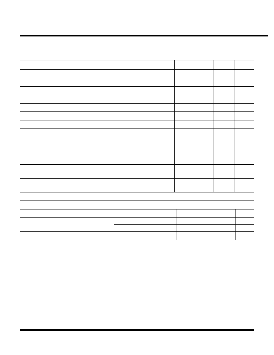
SYMBOL
PARAMETER
TEST CONDITIONS
MIN
TYP
MAX
UNITS
V
IN
Supply Voltage Range
1.8
15
V
I
IN
Supply Current
I
O
= 0 mA, Except I
CONT
170
350
µ
A
I
INS
Standby Current
V
IN
= 8 V, Output off
0.1
µ
A
V
O
Output Voltage
I
O
= 30 mA
2.90
3.00
3.10
V
V
DROP
Dropout Voltage
I
O
= 60 mA
0.18
0.3
V
I
O
Output Current
Note 3
150
170
mA
I
OR
Recommended Output Current
130.0
mA
Line Reg
Line Regulation
V
IN
= 3.5
8.5 V
3.0
20
mV
Load Reg
Load Regulation
I
O
= 5 mA
60 mA
30
60
mV
I
O
= 5 mA
100 mA
80
150
mV
RR
Ripple Rejection
100 mV(rms), f = 400 Hz,
60.0
dB
I
O
= 10
V
O
/
T
A
Temperature Coefficient
I
O
= 10 mA
0.15
mV/
∞
C
-25
∞
C
T
A
+ 75
∞
C
V
NO
Output Noise Voltage
10 Hz < f < 100 kHz,
30
µ
V(rms)
I
O
= 30 mA, Cp = 0.01
µ
F
V
REF
Noise Bypass Terminal Voltage
1.25
V
Control Terminal Specification
I
CONT
Control Current
Output on, V
CONT
= 2.4 V
14
40
µ
A
V
CONT
Control Voltage
Output on
2.4
V
Output off
0.6
V
t
r
Output Rise Time Off
On
I
O
= 30 mA, V
CONT
= 0
2.4 V
0.3
ms
Note 1:
Power dissipation must be derated at rate of 1.6 mW/
∞
C for operation above 25
∞
C . Maximum power dissipation = 400 mW
(When mounted as recommended), and 200 mW in free air.
Note 2:
Output side capacitor should have low ESR at low temperatures if used below 0
∞
C.
Note 3:
I
O
(Output Current) is the measured current when the output voltage drops 0.3 V with respect to V
O
at I
O
= 30 mA.
Note 4:
This measurement (pulse measurement) is with a constant T
J
. The output change due to temperature change is not included.
TK11230 ELECTRICAL CHARACTERISTICS
Test conditions: T
A
= 25
∞
C, V
IN
= 4 V, unless otherwise specified.
Page 4
1-3-96
TK112xx
January, 1996 TOKO, Inc.
SYMBOL
PARAMETER
TEST CONDITIONS
MIN
TYP
MAX
UNITS
V
IN
Supply Voltage Range
1.8
15
V
I
IN
Supply Current
I
O
= 0 mA, Except I
CONT
170
350
µ
A
I
INS
Standby Current
V
IN
= 8 V, Output off
0.1
µ
A
V
O
Output Voltage
I
O
= 30 mA
3.15
3.25
3.35
V
V
DROP
Dropout Voltage
I
O
= 60 mA
0.18
0.3
V
I
O
Output Current
Note 3
150
170
mA
I
OR
Recommended Output Current
130
mA
Line Reg
Line Regulation
V
IN
= 3.75
8.75 V
3.0
20
mV
Load Reg
Load Regulation
I
O
= 5 mA
60 mA
30
60
mV
I
O
= 5 mA
100 mA
80
150
mV
RR
Ripple Rejection
100 mV(rms), f = 400 Hz,
60.0
dB
I
O
= 10 mA
V
O
/
T
A
Temperature Coefficient
I
O
= 10 mA
0.15
mV/
∞
C
-25
∞
C
T
A
+ 75
∞
C
V
NO
Output Noise Voltage
10 Hz < f < 100 kHz,
30
µ
V(rms)
I
O
= 30 mA, Cp = 0.01
µ
F
V
REF
Noise Bypass Terminal Voltage
1.25
V
Control Terminal Specification
I
CONT
Control Current
Output on, V
CONT
= 2.4 V
14
40
µ
A
V
CONT
Control Voltage
Output on
2.4
V
Output off
0.6
V
t
r
Output Rise Time Off
On
I
O
= 30 mA, V
CONT
= 0
2.4 V
0.3
ms
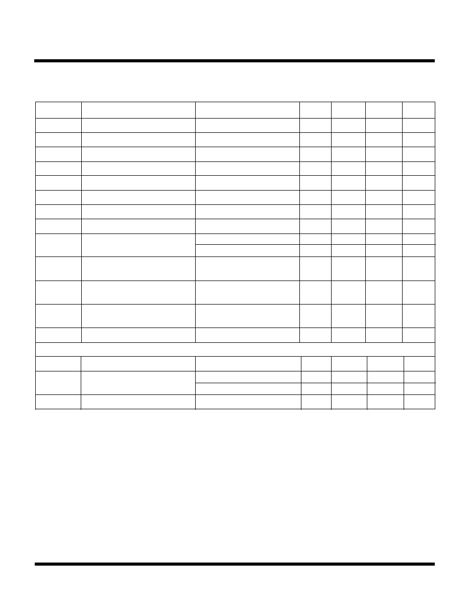
TK11232 ELECTRICAL CHARACTERISTICS
Test conditions: T
A
= 25
∞
C, V
IN
= 4.3 V, unless otherwise specified.
Note 1:
Power dissipation must be derated at rate of 1.6 mW/
∞
C for operation above 25
∞
C . Maximum power dissipation = 400 mW
(When mounted as recommended), and 200 mW in free air.
Note 2:
Output side capacitor should have low ESR at low temperatures if used below 0
∞
C.
Note 3:
I
O
(Output Current) is the measured current when the output voltage drops 0.3 V with respect to V
O
at I
O
= 30 mA.
Note 4:
This measurement (pulse measurement) is with a constant T
J
. The output change due to temperature change is not included.
TK112xx
January, 1996 TOKO, Inc.
Page 5
1-3-96
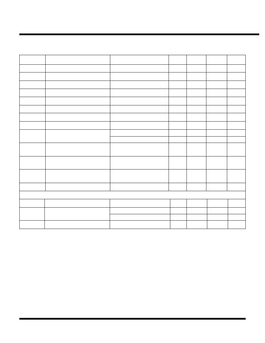
TK11235 ELECTRICAL CHARACTERISTICS
Test conditions: T
A
= 25
∞
C, V
IN
= 4.5 V, unless otherwise specified.
SYMBOL
PARAMETER
TEST CONDITIONS
MIN
TYP
MAX
UNITS
V
IN
Supply Voltage Range
1.8
15
V
I
IN
Supply Current
I
O
= 0 mA, Except I
CONT
170
350
µ
A
I
INS
Standby Current
V
IN
= 8 V, Output off
0.1
µ
A
V
O
Output Voltage
I
O
= 30 mA
3.39
3.5
3.61
V
V
DROP
Dropout Voltage
I
O
= 60 mA
0.18
0.3
V
I
O
Output Current
Note 3
150
170
mA
I
OR
Recommended Output Current
130
mA
Line Reg
Line Regulation
V
IN
= 4
9 V
3.0
20
mV
Load Reg
Load Regulation
I
O
= 5 mA
60 mA
30
60
mV
I
O
= 5 mA
100 mA
80
150
mV
RR
Ripple Rejection
100 mV(rms), f = 400 Hz,
60.0
dB
I
O
= 10 mA
V
O
/
T
A
Temperature Coefficient
I
O
= 10 mA
0.15
mV/
∞
C
-25
∞
C
T
A
+ 75
∞
C
V
NO
Output Noise Voltage
10 Hz < f < 100 kHz,
35
µ
V(rms)
I
O
= 30 mA, Cp = 0.01
µ
F
V
REF
Noise Bypass Terminal Voltage
1.25
V
Control Terminal Specification
I
CONT
Control Current
Output on, V
CONT
= 2.4 V
14
40
µ
A
V
CONT
Control Voltage
Output on
2.4
V
Output off
0.6
V
t
r
Output Rise Time Off
On
I
O
= 30 mA, V
CONT
= 0
2.4 V
0.3
ms
Note 1:
Power dissipation must be derated at rate of 1.6 mW/
∞
C for operation above 25
∞
C. Maximum power dissipation = 400 mW
(When mounted as recommended), and 200 mW in free air.
Note 2:
Output side capacitor should have low ESR at low temperatures if used below 0
∞
C.
Note 3:
I
O
(Output Current) is the measured current when the output voltage drops 0.3 V with respect to V
O
at I
O
= 30 mA.
Note 4:
This measurement (pulse measurement) is with a constant T
J
. The output change due to temperature change is not included.
Page 6
1-3-96
TK112xx
January, 1996 TOKO, Inc.
TK11240 ELECTRICAL CHARACTERISTICS
Test conditions: T
A
= 25
∞
C, V
IN
= 5 V, unless otherwise specified.
SYMBOL
PARAMETER
TEST CONDITIONS
MIN
TYP
MAX
UNITS
V
IN
Supply Voltage Range
1.8
15
V
I
IN
Supply Current
I
O
= 0 mA, Except I
CONT
170
350
µ
A
I
INS
Standby Current
V
IN
= 8 V, Output off
0.1
µ
A
V
O
Output Voltage
I
O
= 30 mA
3.88
4.0
4.12
V
V
DROP
Dropout Voltage
I
O
= 60 mA
0.18
0.3
V
I
O
Output Current
Note 3
150
170
mA
I
OR
Recommended Output Current
130
mA
Line Reg
Line Regulation
V
IN
= 4.5
9.5 V
3.0
20
mV
Load Reg
Load Regulation
I
O
= 5 mA
60 mA
30
60
mV
I
O
= 5 mA
100 mA
80
150
mV
RR
Ripple Rejection
100 mV(rms), f = 400 Hz,
60
dB
I
O
= 10 mA
V
O
/
T
A
Temperature Coefficient
I
O
= 10 mA
0.2
mV/
∞
C
-25
∞
C
T
A
+ 75
∞
C
V
NO
Output Noise Voltage
10 Hz < f < 100 kHz,
40
µ
V(rms)
I
O
= 30 mA, Cp = 0.01
µ
F
V
REF
Noise Bypass Terminal Voltage
1.25
V
Control Terminal Specification
I
CONT
Control Current
Output on, V
CONT
= 2.4 V
14
40
µ
A
V
CONT
Control Voltage
Output on
2.4
V
Output off
0.6
V
t
r
Output Rise Time Off
On
I
O
= 30 mA, V
CONT
= 0
2.4 V
0.3
ms
Note 1:
Power dissipation must be derated at rate of 1.6 mW/
∞
C for operation above 25
∞
C . Maximum power dissipation = 400 mW
(When mounted as recommended), and 200 mW in free air.
Note 2:
Output side capacitor should have low ESR at low temperatures if used below 0
∞
C.
Note 3:
I
O
(Output Current) is the measured current when the output voltage drops 0.3 V with respect to V
O
at I
O
= 30 mA.
Note 4:
This measurement (pulse measurement) is with a constant T
J
. The output change due to temperature change is not included.
TK112xx
January, 1996 TOKO, Inc.
Page 7
1-3-96
SYMBOL
PARAMETER
TEST CONDITIONS
MIN
TYP
MAX
UNITS
V
IN
Supply Voltage Range
1.8
15
V
I
IN
Supply Current
I
O
= 0 mA, Except I
CONT
170
350
µ
A
I
INS
Standby Current
V
IN
= 8 V, Output off
0.1
µ
A
V
O
Output Voltage
I
O
= 30 mA
4.37
4.5
4.63
V
V
DROP
Dropout Voltage
I
O
= 60 mA
0.18
0.3
V
I
O
Output Current
Note 3
150
170
mA
I
OR
Recommended Output Current
130
mA
Line Reg
Line Regulation
V
IN
= 5
10 V
3.0
20
mV
Load Reg
Load Regulation
I
O
= 5 mA
60 mA
30
60
mV
I
O
= 5 mA
100 mA
80
150
mV
RR
Ripple Rejection
100 mV(rms), f = 400 Hz,
60
dB
I
O
= 10 mA
V
O
/
T
A
Temperature Coefficient
I
O
= 10 mA
0.25
mV/
∞
C
-25
∞
C
T
A
+ 75
∞
C
V
NO
Output Noise Voltage
10 Hz < f < 100 kHz,
45
µ
V(rms)
I
O
= 30 mA, Cp = 0.01
µ
F
V
REF
Noise Bypass Terminal Voltage
1.25
V
Control Terminal Specification
I
CONT
Control Current
Output on, V
CONT
= 2.4 V
14
40
µ
A
V
CONT
Control Voltage
Output on
2.4
V
Output off
0.6
V
t
r
Output Rise Time Off
On
I
O
= 30 mA, V
CONT
= 0
2.4 V
0.3
ms
TK11245 ELECTRICAL CHARACTERISTICS
Test conditions: T
A
= 25
∞
C, V
IN
= 5.5 V, unless otherwise specified.
Note 1:
Power dissipation must be derated at rate of 1.6 mW/
∞
C for operation above 25
∞
C . Maximum power dissipation = 400 mW
(When mounted as recommended), and 200 mW in free air.
Note 2:
Output side capacitor should have low ESR at low temperatures if used below 0
∞
C.
Note 3:
I
O
(Output Current) is the measured current when the output voltage drops 0.3 V with respect to V
O
at I
O
= 30 mA.
Note 4:
This measurement (pulse measurement) is with a constant T
J
. The output change due to temperature change is not included.
Page 8
1-3-96
TK112xx
January, 1996 TOKO, Inc.
SYMBOL
PARAMETER
TEST CONDITIONS
MIN
TYP
MAX
UNITS
V
IN
Supply Voltage Range
1.8
15
V
I
IN
Supply Current
I
O
= 0 mA, Except I
CONT
170
350
µ
A
I
INS
Standby Current
V
IN
= 8 V, Output off
0.1
µ
A
V
O
Output Voltage
I
O
= 30 mA
4.61
4.75
4.89
V
V
DROP
Dropout Voltage
I
O
= 60 mA
0.18
0.3
V
I
O
Output Current
Note 3
150
170
mA
I
OR
Recommended Output Current
130
mA
Line Reg
Line Regulation
V
IN
= 5.25
10.25 V
3.0
20
mV
Load Reg
Load Regulation
I
O
= 5 mA
60 mA
30
60
mV
I
O
= 5 mA
100 mA
80
150
mV
RR
Ripple Rejection
100 mV(rms), f = 400 Hz,
60
dB
I
O
= 10 mA
V
O
/
T
A
Temperature Coefficient
I
O
= 10 mA
0.4
mV/
∞
C
-25
∞
C
T
A
+ 75
∞
C
V
NO
Output Noise Voltage
10 Hz < f < 100 kHz,
45
µ
V(rms)
I
O
= 30 mA, Cp = 0.01
µ
F
V
REF
Noise Bypass Terminal Voltage
1.25
V
Control Terminal Specification
I
CONT
Control Current
Output on, V
CONT
= 2.4 V
14
40
µ
A
V
CONT
Control Voltage
Output on
2.4
V
Output off
0.6
V
t
r
Output Rise Time Off
On
I
O
= 30 mA, V
CONT
= 0
2.4 V
0.3
ms
TK11247 ELECTRICAL CHARACTERISTICS
Test conditions: T
A
= 25
∞
C, V
IN
= 5.7 V, unless otherwise specified.
Note 1:
Power dissipation must be derated at rate of 1.6 mW/
∞
C for operation above 25
∞
C. Maximum power dissipation = 400 mW
(When mounted as recommended), and 200 mW in free air.
Note 2:
Output side capacitor should have low ESR at low temperatures if used below 0
∞
C.
Note 3:
I
O
(Output Current) is the measured current when the output voltage drops 0.3 V with respect to V
O
at I
O
= 30 mA.
Note 4:
This measurement (pulse measurement) is with a constant T
J
. The output change due to temperature change is not included.
TK112xx
January, 1996 TOKO, Inc.
Page 9
1-3-96
SYMBOL
PARAMETER
TEST CONDITIONS
MIN
TYP
MAX
UNITS
V
IN
Supply Voltage Range
1.8
15
V
I
IN
Supply Current
I
O
= 0 mA, Except I
CONT
160
350
µ
A
I
INS
Standby Current
V
IN
= 8 V, Output off
0.1
µ
A
V
O
Output Voltage
I
O
= 30 mA
4.85
5.0
515
V
V
DROP
Dropout Voltage
I
O
= 60 mA
0.18
0.3
V
I
O
Output Current
Note 3
150
170
mA
I
OR
Recommended Output Current
130
mA
Line Reg
Line Regulation
V
IN
= 5.5
10.5 V
3.0
20
mV
Load Reg
Load Regulation
I
O
= 5 mA
60 mA
30
60
mV
I
O
= 5 mA
100 mA
80
150
mV
RR
Ripple Rejection
100 mV(rms), f = 400 Hz,
60
dB
I
O
= 10 mA
V
O
/
T
A
Temperature Coefficient
I
O
= 10 mA
0.4
mV/
∞
C
-25
∞
C
T
A
+ 75
∞
C
V
NO
Output Noise Voltage
10 Hz < f < 100 kHz,
50
µ
V(rms)
I
O
= 30 mA, Cp = 0.01
µ
F
V
REF
Noise Bypass Terminal Voltage
1.25
V
Control Terminal Specification
I
CONT
Control Current
Output on, V
CONT
= 2.4 V
14
40
µ
A
V
CONT
Control Voltage
Output on
2.4
V
Output off
0.6
V
t
r
Output Rise Time Off
On
I
O
= 30 mA, V
CONT
= 0
2.4 V
0.3
ms
TK11250 ELECTRICAL CHARACTERISTICS
Test conditions: T
A
= 25
∞
C, V
IN
= 6 V, unless otherwise specified.
Note 1:
Power dissipation must be derated at rate of 1.6 mW/
∞
C for operation above 25
∞
C. Maximum power dissipation = 400 mW
(When mounted as recommended), and 200 mW in free air.
Note 2:
Output side capacitor should have low ESR at low temperatures if used below 0
∞
C.
Note 3:
I
O
(Output Current) is the measured current when the output voltage drops 0.3 V with respect to V
O
at I
O
= 30 mA.
Note 4:
This measurement (pulse measurement) is with a constant T
J
. The output change due to temperature change is not included.
Page 10
1-3-96
TK112xx
January, 1996 TOKO, Inc.
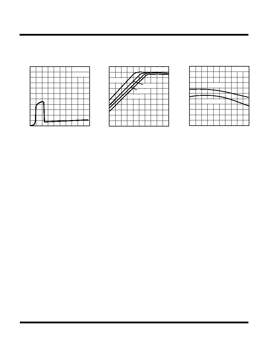
TK112XX∑ TPC01
IO (mA)
V
DROP
(V)
0
50
100
DROPOUT VOLTAGE vs.
LOAD CURRENT
0.5
0.4
0.3
0.2
0.1
T = 25
∞
C
A
0
TK11250
TK112XX ∑ TPC02
IO (mA)
V
O
(V)
0
100
200
OUTPUT VOLTAGE vs.
SHORT CIRCUIT CURRENT
T = 25
∞
C
A
0
1
2
3
4
5
V
IN
= V
O
+ 1
TK11230
TK11250
TK11220
TEST CIRCUIT
TK112XX ∑ TPC06
LINE TRANSIENT RESPONSE
TA = 25
∞
C
V
CC
VO
10 mV/DIV
50
µ
s/DIV
DV = 1 V
TK112XX ∑ TPC04
V (V)
CC
I CONT
(pA)
0
QUIESCENT CURRENT vs.
INPUT VOLTAGE
T = 25
∞
C
A
0
100
200
10
20
TK112XX ∑ TPC05
RIPPLE REJECTION
T = 25
∞
C
A
100
1k
10k
100k
LEVEL (dB)
0
-50
-100
HZ
TK112XX ∑ TPC03
VCONT (V)
I CONT
(
µ
A)
0
CONTROL TERMINAL CIRCUIT CURRENT vs.
CONTROL TERMINAL VOLTAGE
TA= 25
∞
C
0
10
20
30
40
50
1
2
3
4
5
R
CONT
= 0
RCONT = 0
300 K
75 K
150 K
VO
75 K
150 K
300 K
T
A
= 25
∞
C unless otherwise specified.
1
4
5
6
2
3
S
V
IN
V
A
A
V
S
S
S
V
O
I
OUT
V
IN
V
OUT
1
µ
F
10
µ
F
I
CONT
CONT
CONT
NOTE: CONNECT PINS 2 AND 5 TO
GND FOR MAXIMUM HEAT CONDUCTION.
+
+
_
+
_
.01
µ
F
Noise Bypass
+
TYPICAL PERFORMANCE CHARACTERISTICS
TK112xx
January, 1996 TOKO, Inc.
Page 11
1-3-96
TK12XX ∑ TPC07
LOAD TRANSIENT RESPONSE
TA = 25
∞
C
I
O
VO
10 mV/DIV
50
µ
s/DIV
IO = 60 mA
IO = 0 mA
TK112XX ∑ TPC08
SHUTDOWN CONTROL (OFF-ON)
TA = 25
∞
C
SD
VO
50
µ
s/DIV
C
L
=10
µ
F
C
L
=3.3
µ
F
C
P
=.001
C
P
=.1
C
P
=.01
C
P
=.001
C
P
=.1
C
P
=.01
TK112XX ∑ TPC09
NOISE LEVEL vs.
BYPASS CAPACITOR (pF)
TA = 25
∞
C
Cp
1 pF 10 pF 100 pF .001
µ
F .01
µ
F .1
µ
F
200
150
100
50
0
NOISE (
µ
V)
TK11250
TK11220
C
L
= 3.3
µ
F
C
L
= 3.3
µ
F
C
L
= 10
µ
F
C
L
= 10
µ
F
IO = 60 mA
0
TK112XX ∑ TPC13
CONTROL PIN VOLTAGE (V)
≠50
TA (
∞
C)
100
0
50
CONTROL PIN VOLTAGE vs.
TEMPERATURE
2.0
1.0
120
TK112XX ∑ TPC14
OUTPUT CURRENT (mA)
≠50
100
0
50
OUTPUT CURRENT vs.
TEMPERATURE
140
160
180
200
TA (
∞
C)
0
2.5
TK112XX ∑ TPC10
5
QUIESCENT CURRENT (mA)
≠50
TA (
∞
C)
100
VIN = VO +1V
IO = 60 mA
0
50
QUIESCENT CURRENT vs.
TEMPERATURE
IO = 30 mA
0
TK112XX ∑ TPC11
DROP OUT VOLTAGE (mV)
≠50
TA (
∞
C)
100
0
50
DROPOUT VOLTAGE vs.
TEMPERATURE
500
400
300
200
100
IO = 60 mA
IO = 30 mA
0
TK112XX ∑ TPC12
CONTROL PIN CURRENT (
µ
A)
≠50
TA (
∞
C)
100
0
50
CONTROL PIN CURRENT vs.
TEMPERATURE
50
40
30
20
10
VCONT = 5 V
VCONT = 2.4 V
TYPICAL PERFORMANCE CHARACTERISTICS (CONT.)
T
A
= 25
∞
C unless otherwise specified.
Page 12
1-3-96
TK112xx
January, 1996 TOKO, Inc.
OUTPUT VOLTAGE vs.
INPUT VOLTAGE
2.25
3.25
VIN (V)
2.75
2.75
V
O
(V
)
2.25
1.75
IO = 0 mA
60 mA
90 mA
30 mA
227-5
OUTPUT VOLTAGE vs.
TEMPERATURE
-50
100
TA(∞C)
2.70
2.80
0
V
O
(V)
2.75
50
IO = 30 mA
227-6
60 mA
TK112XX ∑ TPC28
IO (mA)
I Q
(mA)
0
50
100
5
QUIESCENT CURRENT vs.
LOAD CURRENT
10
0
VIN = 4.0 V
TA = 25
∞
C
TK112XX∑ TPC29
VIN (V)
V
O
(V)
0
10
20
2.6
OUTPUT VOLTAGE vs.
INPUT VOLTAGE
TA = 25
∞
C
2.7
2.8
2.9
3.0
3.1
IO = 0 mA
TK11230
TYPICAL PERFORMANCE CHARACTERISTICS (CONT.)
TK11227
QUIESCENT CURRENT vs.
OUTPUT CURRENT
0
100
IO (mA)
0
10
50
I Q
(mA)
5
227-2
LOAD REGULATION
0
100
IO (mA)
2.55
2.95
50
V
O
(V)
2.75
227-1
INPUT CURRENT (NO LOAD) vs.
INPUT VOLTAGE
0
20
VIN (V)
2
10
I IN
(mA)
1
0
227-4
TK112XX ∑ TPC27
IO (mA)
V
O
(V)
0
50
100
2.8
3.0
3.2
OUTPUT VOLTAGE vs.
OUTPUT CURRENT
TA = 25
∞
C
VIN = 3.1 V
OUTPUT VOLTAGE vs.
INPUT VOLTAGE
0
20
VIN (V)
2.85
10
V
O
(V)
2.75
2.65
2.55
2.45
2.35
227-3
T
A
= 25
∞
C unless otherwise specified.
TK112xx
January, 1996 TOKO, Inc.
Page 13
1-3-96
TK11232
TK11230 (CONT.)
TYPICAL PERFORMANCE CHARACTERISTICS (CONT.)
OUTPUT VOLTAGE vs.
SUPPLY VOLTAGE
2.8
3.7
VIN (V)
3.2
3.2
V
O
(V)
2.4
IO = 0 mA
60 mA
90 mA
30 mA
232-5
3.0
2.8
2.6
INPUT CURRENT (NO LOAD) vs.
INPUT VOLTAGE
0
20
VIN (V)
2
10
I IN
(mA)
1
0
232-4
TK112XX ∑ TPC30
VIN (V)
I IN
(
µ
A)
0
10
20
1
INPUT CURRENT vs.
INPUT VOLTAGE
2
0
IO = 0 mA
TA = 25
∞
C
TK112XX ∑ TPC31
VIN (V)
V
O
(V)
2.5
3.0
3.5
2.0
2.5
OUTPUT VOLTAGE vs.
INPUT VOLTAGE
3.0
IO = 0 mA
TA = 25
∞
C
IO = 30 mA
IO = 60 mA
IO = 90 mA
2.95
3.0
TK112XX ∑ TPC32
3.05
V
O
(V)
≠50
TA (
∞
C)
80
VIN = 4.0 V
IO = 30 mA
0
50
OUTPUT VOLTAGE vs.
TEMPERATURE
IO = 60 mA
OUTPUT VOLTAGE vs.
INPUT VOLTAGE
0
20
VIN (V)
3.3
10
V
O
(V)
3.2
3.1
3.0
2.9
232-3
QUIESCENT CURRENT vs.
OUTPUT CURRENT
0
100
IO (mA)
0
10
50
I Q
(mA)
5
232-2
LOAD REGULATION
0
100
IO (mA)
3.0
3.45
50
V
O
(V)
3.25
232-1
OUTPUT VOLTAGE vs.
TEMPERATURE
-50
100
TA (∞C)
3.20
3.30
0
V
O
(V)
3.25
50
IO = 30 mA
60 mA
232-6
T
A
= 25
∞
C unless otherwise specified.
Page 14
1-3-96
TK112xx
January, 1996 TOKO, Inc.
INPUT CURRENT (NO LOAD vs.
SUPPLY VOLTAGE
0
20
VIN (V)
2
10
I IN
(mA)
1
0
235-4
OUTPUT VOLTAGE vs.
INPUT VOLTAGE
3.0
4.0
VIN (V)
3.5
3.5
V
O
(V
)
2.5
IO = 0 mA
60 mA
90 mA
30 mA
235-5
3.0
LOAD REGULATION
0
100
IO (mA)
3.8
4.2
50
V
O
(V)
4.0
240-1
QUIESCENT CURRENT vs.
OUTPUT CURRENT
0
100
IO (mA)
0
10
50
I Q
(mA)
5
240-2
TK11240
OUTPUT VOLTAGE vs.
INPUT VOLTAGE
0
20
VIN (V)
4.1
10
V
O
(V)
4.0
3.9
3.8
3.7
240-3
3.6
OUTPUT VOLTAGE vs.
TEMPERATURE
-50
100
TA (∞C)
3.45
3.55
0
V
O
(V)
3.5
50
IO = 30 mA
60 mA
235-6
TK11235
QUIESCENT CURRENT vs.
OUTPUT CURRENT
0
100
IO (mA)
0
10
50
I Q
(mA)
5
235-2
LOAD REGULATION
0
100
IO (mA)
3.3
3.7
50
V
O
(V)
3.5
235-1
OUTPUT VOLTAGE vs.
INPUT VOLTAGE
0
20
VIN (V)
3.6
10
V
O
(V)
3.5
3.4
3.3
3.2
3.1
235-3
TYPICAL PERFORMANCE CHARACTERISTICS (CONT.)
T
A
= 25
∞
C unless otherwise specified.
TK112xx
January, 1996 TOKO, Inc.
Page 15
1-3-96
OUTPUT VOLTAGE vs.
INPUT VOLTAGE
0
20
VIN (V)
4.6
10
V
O
(V)
4.5
4.4
4.3
4.2
245-3
4.1
QUIESCENT CURRENT vs.
OUTPUT CURRENT
0
100
IO (mA)
0
10
50
I Q
(mA)
5
245-2
INPUT CURRENT (NO LOAD) vs.
INPUT VOLTAGE
0
20
VIN (V)
2
10
I IN
(mA)
1
0
245-4
OUTPUT VOLTAGE vs.
INPUT VOLTAGE
4.0
5.0
VIN (V)
4.5
4.5
V
O
(V
)
3.5
IO = 0 mA
60 mA
90 mA
30 mA
245-5
4.0
OUTPUT VOLTAGE vs.
TEMPERATURE
-50
100
TA (∞C)
4.45
4.55
0
V
O
(V)
4.5
50
IO = 30 mA
60 mA
245-6
TK11240 (CONT.)
TK11245
SUPPLY VOLTAGE vs.
INPUT CURRENT (NO LOAD)
0
20
VCC (V)
2
10
I CC
(mA)
1
0
240-4
SUPPLY VOLTAGE vs.
OUTPUT VOLTAGE
3.5
4.5
VCC (V)
4.0
4.0
V
O
(V)
3.0
IO = 0 mA
60 mA
90 mA
30 mA
240-5
3.5
TEMPERATURE vs.
OUTPUT VOLTAGE
-50
100
TA(∞C)
3.95
4.05
0
V
O
(V)
4.0
50
IO = 30 mA
60 mA
240-6
LOAD REGULATION
0
100
IO (mA)
4.3
4.7
50
V
O
(V)
4.5
245-1
TYPICAL PERFORMANCE CHARACTERISTICS (CONT.)
T
A
= 25
∞
C unless otherwise specified.
Page 16
1-3-96
TK112xx
January, 1996 TOKO, Inc.
TYPICAL PERFORMANCE CHARACTERISTICS (CONT.)
TK11250
INPUT CURRENT (NO LOAD) vs.
INPUT VOLTAGE
0
20
VIN (V)
2
10
I IN
(mA)
1
0
247-4
OUTPUT VOLTAGE vs.
INPUT VOLTAGE
4.25
5.25
VIN (V)
4.75
4.75
V
O
(V
)
3.75
60 mA
90 mA
30 mA
247-5
4.25
IO = 0 mA
OUTPUT VOLTAGE vs .
TEMPERATURE
-50
100
TA (∞C)
4.70
4.80
0
V
O
(V)
4.75
50
IO = 30 mA
60 mA
247-6
TK112XX ∑ TPC33
IO (mA)
V
O
(V)
0
50
100
4.8
5.0
5.2
OUTPUT VOLTAGE vs.
OUTPUT CURRENT
TA = 25
∞
C
VIN = 6.0 V
TK112XX ∑ TPC34
IO (mA)
I Q
(mA)
0
50
100
5
QUIESCENT CURRENT vs.
LOAD CURRENT
10
0
VIN = 6.0 V
TA = 25
∞
C
QUIESCENT CURRENT vs.
OUTPUT CURRENT
0
100
IO (mA)
0
10
50
I Q
(mA)
5
247-2
OUTPUT VOLTAGEvs.
SUPPLY VOLTAGE
0
20
VIN (V)
4.85
10
V
O
(V)
4.75
4.65
4.55
4.45
247-3
4.35
TK11247
TK112XX∑ TPC35
VIN (V)
V
O
(V)
0
10
20
4.6
OUTPUT VOLTAGE vs.
INPUT VOLTAGE
I = 0 mA
O
TA = 25
∞
C
4.7
4.8
4.9
5.0
5.1
LOAD REGULATION
0
100
IO (mA)
4.55
4.95
50
V
O
(V)
4.75
247-1
T
A
= 25
∞
C unless otherwise specified.
TK112xx
January, 1996 TOKO, Inc.
Page 17
1-3-96
TYPICAL PERFORMANCE CHARACTERISTICS (CONT.)
TK11250 (CONT.)
4.95
5.0
TK112XX ∑ TPC38
5.05
V
O
(V)
≠50
T ( C)
∞
A
80
VIN = 6.0 V
IO = 30 mA
0
50
OUTPUT VOLTAGE vs.
TEMPERATURE
IO = 60 mA
TK112XX ∑ TPC37
VIN ( V)
V
O
(V)
4.5
5.0
5.5
4.0
4.5
OUTPUT VOLTAGE vs.
INPUT VOLTAGE
5.0
IO = 0 mA
TA = 25
∞
C
IO = 30 mA
IO = 60 mA
IO = 90 mA
TK112XX ∑ TPC36
VIN (V)
I IN
(
µ
A)
0
10
20
1
INPUT CURRENT vs.
INPUT VOLTAGE
2
0
TA = 25
∞
C
IO = 0 mA
DEFINITION AND EXPLANATION OF TECHNICAL TERMS
LINE REGULATION (LINE REG)
Line regulation is the relationship between change in
output voltage due to a change in input voltage.
LOAD REGULATION (LOAD REG)
Load regulation is the relationship between change in
output voltage due to a change in load current.
DROP OUT VOLTAGE (V
DROP
)
This is a measure of how well the regulator performs as the
input voltage decreases. The smaller the number, the
further the input voltage can decrease before regulation
problems occur. Nominal output voltage is first measured
when V
IN
= V
O
+ 1 at a chosen load current. When the
output voltage has dropped 100 mV from the nominal, V
IN
- V
O
is the dropout voltage. This voltage is affected by load
current and junction temperature.
OUTPUT NOISE VOLTAGE
This is the effective AC voltage that occurs on the output
voltage under the condition where the input noise is low and
with a given load, filter capacitor, and frequency range.
THERMAL PROTECTION
This is an internal feature which turns the regulator off when
the junction temperature rises above 150
∞
C. After the
regulator turns off, the temperature drops and the regulator
output turns back on. Under certain conditions, the output
waveform may appear to be an oscillation as the output
turns off and on and back again in succession.
PACKAGE POWER DISSIPATION (P
D
)
This is the power dissipation level at which the thermal
sensor is activated. The IC contains an internal thermal
sensor which monitors the junction temperature. When the
junction temperature exceeds the monitor threshold of
150
∞
C, the IC is shutdown. The junction temperature rises
as the difference between the input power (V
IN
X I
IN
) and
the output power (V
O
X I
O
) increases. The rate of tempera-
ture rise is greatly affected by the mounting pad configura-
tion on the PCB, the board material, and the ambient
temperature. When the IC mounting has good thermal
conductivity, the junction temperature will be low even if the
power dissipation is great. When mounted onthe recom-
mended mounting pad, the power dissipation of the SOT-
23L is increased to 400 mW. For operation at ambient
temperatures over 25
∞
C, the power dissipation of the SOT-
23L device should be derated at 3.2 mW/
∞
C. To determine
the power dissipation for shutdown when mounted, attach
the device on the actual PCB and deliberately increase the
output current (or raise the input voltage) until the thermal
protection circuit is activated. Calculate the power dissipa-
tion of the device by subtracting the output power from the
input power. These measurements should allow for the
ambient temperature of the PCB. The value obtained from
PD/(150
∞
C - T
A
) is the derating factor. The PCB mounting
pad should provide maximum thermal conductivity in order
to maintain low device temperatures. As a general rule, the
T
A
= 25
∞
C unless otherwise specified.
Page 18
1-3-96
TK112xx
January, 1996 TOKO, Inc.
lower the temperature, the better the reliability of the
device. The Thermal resistance when mounted is ex-
pressed as follows:
T
J
= 0
JA
X P
D
+ T
A
For Toko ICs, the internal limit for junction temperature is
150
∞
C. If the ambient temperature, T
A
is 25
∞
C, then:
150
∞
C = 0
JA
X P
D
+ 25
∞
C
0
JA
X P
D
= 125
∞
C
0
JA
= 125
∞
C/ P
D
P
D
is the value when the thermal sensor is activated. A
simple way to determine PD is to calculate V
IN
X I
IN
when
the output side is shorted. Input current gradually falls as
temperature rises. You should use the value when thermal
equilibrium is reached.
The range of currents usable can also be found from the
graph below.
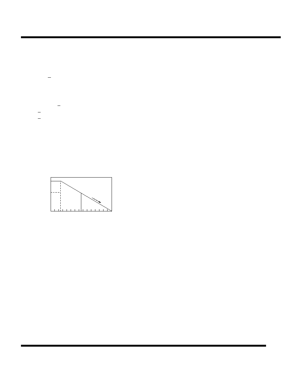
PD
Dpd
25
50
75
150
(mW)
T (∞C)
3
6
5
4
Procedure:
1.)
Find P
D
2.)
P
D1
is taken to be P
D
X (
0.8 ~ 0.9)
3.)
Plot P
D1
against 25
∞
C
4.)
Connect P
D1
to the point corresponding to the
150
∞
C with a straight line.
5.)
In design, take a vertical line from the maximum
operating temperature (e.g. 75
∞
C) to the derating
curve.
6.)
Read off the value of P
D
against the point at which
the vertical line intersects the derating curve. This
is taken as the maximum power dissipation, D
PD
.
The maximum operating current is I
O
X (D
PD
/(V
IN(MAX)
-
V
O
).
DEFINITION AND EXPLANATION OF TECHNICAL TERMS (CONT.)
INPUT/OUTPUT DECOUPLING CAPACITOR CONSIDER-
ATIONS
Voltage regulators require input and output decoupling
capacitors. The required value of these capacitors vary
with application. Capacitors made by different manufactur-
ers can have different characteristics, particularly with
regard to high frequencies and equivalent resistance (ESR)
over temperature. The type of capacitor is also important.
For example, a 5.6
µ
F aluminum electrolytic may be re-
quired for a certain application. If a tantalum capacitor is
used, a lower value of 3.3
µ
F would be adequate. It is
important to consider the temperature characteristics of the
decoupling capacitors. While Toko regulators are de-
signed to operate as low as -30
∞
C, many capacitors will not
operate properly at this temperature. The capacitance of
aluminum electrolytic capacitors may decrease to 0 at low
temperatures. This may cause oscillation on the output of
the regulator since some capacitance is required to guar-
antee stability. Thus, it is important to consider the charac-
teristics of the capacitor over temperature when selection
decoupling capacitors. The ESR is another important
parameter. The ESR will increase with temperature but low
ESR capacitors are often larger and more costly. In
general, Tantalum capacitors offer lower ESR than alumi-
num electrolytic, but new low ESR aluminum electrolytic
capacitors are now available from several manufacturers.
Usually a bench test is sufficient to determine the minimum
capacitance required for a particular application. After
taking thermal characteristics and tolerance into account,
the minimum capacitance value should be approximately
two times this value. The recommended minimum capaci-
tance for the TK112xx is 3.3
µ
F. Please note that linear
regulators with a low dropout voltage have high internal
loop gains which requires care in guarding against oscilla-
tion caused by insufficient decoupling capacitance. The
use of high quality decoupling capacitors suited for your
application will guarantee proper operation of the circuit.
NOISE BYPASS CAPACITOR SECTION
The noise bypass capacitor (C
P
) should be connected as
close as possible to pin 3 and ground. The recommended
value for C
P
is 0.01
µ
F. The noise bypass terminal has a
high impedance and care should be taken if the noise
bypass capacitor is not used. This terminal is susceptible
to external noise and oscillation can occur when C
P
is not
used and the solder pad for this pin is made too large.

TK112xx
January, 1996 TOKO, Inc.
Page 19
1-3-96
1.) Disabling the control pin
Connect control terminal to V
IN
through a resistor (R).
Higher resistance values are good for reducing quiescent
current but this can cause the regulator to shut down at
lower input voltages. See Figure A.
+
1 µF
R
+
10 µF
V
O
V
IN
C
P
= 10 nF
1
2
3
6
5
4
Figure A
2.) Using the control function
Turn on the regulator by setting the control pin voltage to
2.4 V or higher. Turn off the regulator by pulling the control
pin below 0.6 V. The regulator can also be controlled
directly from a TTL or CMOS device. See Figure B.
+
1
µF
+
10 µF
V
O
V
IN
C
P
= 10 nF
1
3
6
2
5
4
R
Figure B
3.) Microprocessor/Logic Control
112XX
Cont
+
VO
GND
+
VIN
Microprocessor
The Input and Control current in the off mode are less than
200 pA.
APPLICATION INFORMATION
0
R
300 k
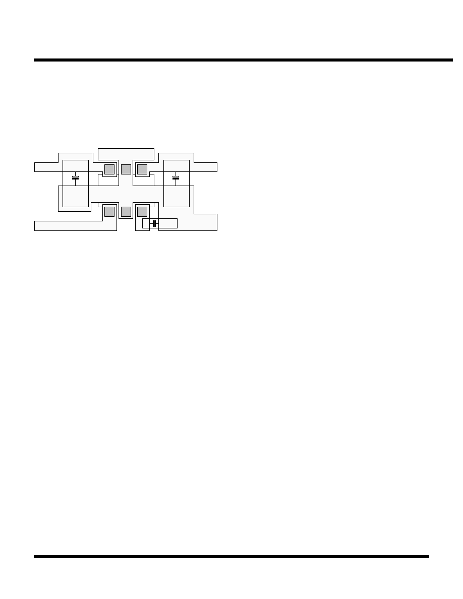
4.) Parallel connection for ON/OFF control
11250
V
IN
Cont
V
O
GND
11230
V
IN
Cont
V
O
GND
11220
V
IN
Cont
V
O
GND
+
+
+
5 V
3 V
2 V
+
+
RS
On/Off
0.1 µF
0.1 µF
V
IN
To reduce IC power dissipation, connect a resistor, R
S
, in
series with V
IN
for the lower output voltage devices. This
will prevent thermal shutdown due to excessive power
dissipation.
5.) Constant current load
112XX
Cont
+
VO
GND
+
VIN
+
R
ON/OFF
When there is a large ouput current, the quiescent current
also increases, and the difference becomes larger. When
using the ON/OFF control, the terminal voltage should be
set 2.4 V higher than the GND terminal of the IC. When the
ON/OFF control is not being used, connect it to V
IN
.
Page 20
1-3-96
TK112xx
January, 1996 TOKO, Inc.
APPLICATION INFORMATION (CONT.)
6.) Heat dissipation
Make the copper pattern as large as possible to provide
good heat dissipation (pin 5 is the heatsink).
Maximum power dissipation = 400 mW (When mounted as
recommended) See Figure C.
+
+
GND
Figure C
7.) Handling molded resin packages
All plastic molded packages absorb some moisture from
the air. If moisture absorption occurs prior to soldering the
devise into the printed circuit board, increased separation
of the lead from the plastic molding may occur, degrading
the moisture barrier characteristics of the device. This
property of plastic molding compounds should not be
overlooked, particularly in the case of very small packages,
where the plastic is very thin. In order to preserve the
original moisture barrier properties of the package, devices
are stored and shipped in moisture proof bags, filled with
dry air. The bags should not be opened or damaged prior
to the actual use of the devices. If this is unavoidable, the
devices should be stored in a low relative humidity environ-
ment (40 to 65%) or in an enclosed environment with
desiccant.
TK112xx
January, 1996 TOKO, Inc.
Page 21
1-3-96
Marking Information
11227
P2
11230
P3
11232
P
3
11235
P
3
11240
P4
11245
P
4
11247
P4
11250
P5
© 1993 Toko America, Inc.
All Rights Reserved
Printed in U.S.A.
IC-114-TK112
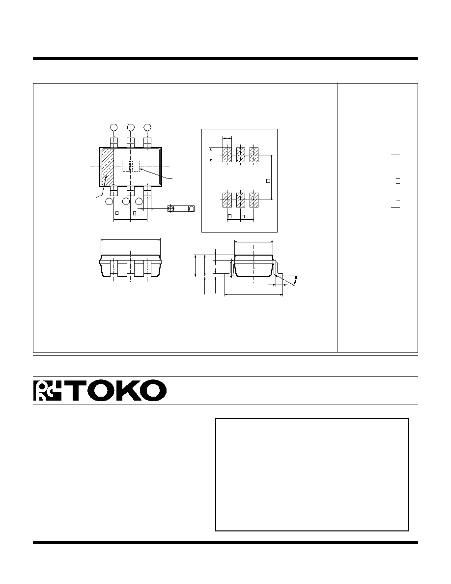
PACKAGE OUTLINE
The information furnished by TOKO, Inc. is believed to be accurate and reliable. However, TOKO reserves the right to make changes or improvements in the design, specification or manufacture of its products without further notice. TOKO
does not assume any liability arising from the application or use of any product or circuit described herein, nor for any infringements of patents or other rights of third parties which may result from the use of its products. No license is granted
by implication or otherwise under any patent or patent rights of TOKO, Inc.
YOUR LOCAL REPRESENTATIVE IS:
TOKO America, Inc.
1250 Feehanville Dr.
Mt. Prospect, ILL 60056
Tel: 1(800) PIK-TOKO
Fax: 1(847) 699-1194
(Pin 2 and pin 5 should be
grounded for heat dissipation)
0.95
0.95
0.4
e
e
0.1
M
3.4
1.25
1.2
0.05
0.15
0.3
3.3
2.2
0.4
+0.1
-0.05
± 0.2
±
0.2
± 0.2
±
0.05
± 0.3
+0.1
-0.05
0.95
0.95
3.2
e
e
e
1
0.6
1.0
±0.15
+0.15
- 0
Unit:mm
Recommended Mount Pad
1
2
3
4
5
6
30∞ Max
Orientation Mark
Marking
Information
SOT23L