TK113xxBM/U
April 2000 TOKO, Inc.
Page 1
ORDERING INFORMATION
TAPE/REEL CODE
L: Tape Left (SOT23L)
B: Tape Left (SOT89)
TEMP. CODE:
C: -30 to +80
∞
C
I: -40 to +85
∞
C
Tape/Reel Code
TK113 B
Voltage Code
Package Code
PACKAGE CODE:
M: SOT23L
U: SOT89
VOLTAGE CODE
20 = 2.0 V
37 = 3.7 V
21 = 2.1 V
38 = 3.8 V
22 = 2.2 V
39 = 3.9 V
23 = 2.3 V
40 = 4.0 V
24 = 2.4 V
41 = 4.1 V
25 = 2.5 V
42 = 4.2 V
26 = 2.6 V
43 = 4.3 V
27 = 2.7 V
44 = 4.4 V
28 = 2.8 V
45 = 4.5 V
29 = 2.9 V
46 = 4.6 V
30 = 3.0 V
47 = 4.7 V
31 = 3.1 V
48 = 4.8 V
32 = 3.2 V
49 = 4.9 V
33 = 3.3 V
50 = 5.0 V
34 = 3.4 V
55 = 5.5 V
35 = 3.5 V
60 = 6.0 V
36 = 3.6 V
80 = 8.0 V
Temp. Code
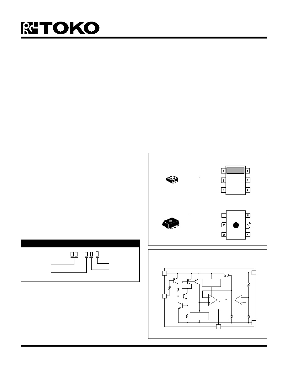
NOISE
BYPASS
VIN
VOUT
THERMAL
PROTECTION
BANDGAP
REFERENCE
CONTROL
GND
VOLTAGE REGULATOR WITH ON/OFF SWITCH
FEATURES
s
High Voltage Precision at
±
2.0%
s
Active Low On/Off Control
s
Very Low Dropout Voltage 80 mV at 30 mA
s
Very Low Noise
s
Very Small SOT23L or SOT89 Surface Mount
Packages
s
Internal Thermal Shutdown
s
Short Circuit Protection
APPLICATIONS
s
Battery Powered Systems
s
Cellular Telephones
s
Pagers
s
Personal Communications Equipment
s
Portable Instrumentation
s
Portable Consumer Equipment
s
Radio Control Systems
s
Toys
s
Low Voltage Systems
BLOCK DIAGRAM
TK113xxB
20P
GND
CONTROL
VOUT
VIN
NOISE BYPASS
GND
VOUT
GND
NOISE BYPASS
GND
CONTROL
VIN
DESCRIPTION
The TK113xxB is a low dropout linear regulator with a built-
in electronic switch. The device is in the "on" state when
the control pin is pulled to a low level. An external capacitor
can be connected to the noise bypass pin to lower the
output noise level to 30
µ
Vrms.
An internal PNP pass transistor is used to achieve a low
dropout voltage of 80 mV (typ.) at 30 mA load current. The
TK113xxB has a very low quiescent current of 170
µ
A at no
load and 1 mA with a 30 mA load. The standby current is
typically 100 nA. The internal thermal shut down circuitry
limits the junction temperature to below 150
∞
C. The load
current is internally monitored and the device will shut
down in the presence of a short circuit or overcurrent
condition at the output.
The TK113xxB is available in either 6-pin SOT23L or 5-pin
SOT89 surface mount packages.
SOT23L
SOT89
TK113xxBM/U
Page 2
April 2000 TOKO, Inc.
ABSOLUTE MAXIMUM RATINGS (V
OUT
2.0 V)
Supply Voltage ......................................................... 16 V
Output Current .................................................... 260 mA
Power Dissipation SOT-23L (Note 1) ............... 600 mW
Power Dissipation SOT-23L (Note 1) ............... 900 mW
Reverse Bias ............................................................ 10 V
Storage Temperature Range ................... -55 to +150
∞
C
Operating Temperature Range .................. -30 to +80
∞
C
Voltage Range ............................................ 1.8 to 14.5 V
Operating Junction Temperature .......................... 150
∞
C
TK113xxBM/UC ELECTRICAL CHARACTERISTICS (V
OUT
2.0 V)
Test conditions: T
A
= 25
∞
C, unless otherwise specified.
Note 1: When mounted as recommended. Derate at 4.8 mW/
∞
C for SOT-23L and 6.4 mW/
∞
C for SOT-89 packages for operation above 25
∞
C.
Note 2: Refer to "Definition of Terms."
Note 3: Ripple rejection and noise voltage are affected by the value and characteristics of the capacitor used.
Note 4: Output noise voltage can be reduced by connecting a capacitor to a noise pass terminal.
Gen. Note: Parameters with min. or max. values are 100% tested at T
A
= 25
∞
C.
L
O
B
M
Y
S
R
E
T
E
M
A
R
A
P
S
N
O
I
T
I
D
N
O
C
T
S
E
T
N
I
M
P
Y
T
X
A
M
S
T
I
N
U
I
Q
t
n
e
r
r
u
C
t
n
e
c
s
e
i
u
Q
I
T
U
O
I
g
n
i
d
u
l
c
x
E
,
A
m
0
=
T
N
O
C
0
7
1
0
5
2
A
µ
I
Y
B
T
S
t
n
e
r
r
u
C
y
b
d
n
a
t
S
V
N
I
F
F
O
t
u
p
t
u
O
,
V
8
=
1
.
0
A
µ
V
T
U
O
e
g
a
t
l
o
V
t
u
p
t
u
O
I
T
U
O
A
m
0
3
=
1
e
l
b
a
T
e
e
S
V
g
e
R
e
n
i
L
n
o
i
t
a
l
u
g
e
R
e
n
i
L
V
T
U
O
)
2
e
t
o
N
(
,
V
5
.
5
0
.
3
0
2
V
m
V
T
U
O
)
2
e
t
o
N
(
,
V
6
.
5
5
1
0
4
V
m
g
e
R
d
a
o
L
n
o
i
t
a
l
u
g
e
R
d
a
o
L
I
T
U
O
)
2
e
t
o
N
(
,
A
m
0
6
o
t
1
=
6
0
3
V
m
I
T
U
O
)
2
e
t
o
N
(
,
A
m
0
0
1
o
t
1
=
8
1
0
6
V
m
I
T
U
O
)
2
e
t
o
N
(
,
A
m
0
5
1
o
t
1
=
3
2
0
9
V
m
V
P
O
R
D
e
g
a
t
l
o
V
t
u
o
p
o
r
D
I
T
U
O
)
2
e
t
o
N
(
,
A
m
0
6
=
2
1
.
0
0
2
.
0
V
I
T
U
O
)
2
e
t
o
N
(
,
A
m
0
5
1
=
6
2
.
0
9
3
.
0
V
I
T
U
O
t
n
e
r
r
u
C
t
u
p
t
u
O
s
u
o
u
n
i
t
n
o
C
)
2
e
t
o
N
(
0
5
1
A
m
I
)
E
S
L
U
P
(
T
U
O
t
n
e
r
r
u
C
t
u
p
t
u
O
e
s
l
u
P
e
l
c
y
c
y
t
u
d
%
5
.
2
1
,
e
s
l
u
p
s
m
5
0
8
1
A
m
R
R
n
o
i
t
c
e
j
e
R
e
l
p
p
i
R
C
,
z
H
0
0
4
=
f
L
C
,
F
µ
0
1
=
N
,
F
µ
1
.
0
=
V
N
I
V
=
T
U
O
I
,
V
5
.
1
+
T
U
O
,
A
m
0
3
=
V
E
L
P
P
I
R
)
3
e
t
o
N
(
,
s
m
r
V
m
0
0
1
=
0
6
B
d
V
O
N
e
g
a
t
l
o
V
e
s
i
o
N
t
u
p
t
u
O
z
H
0
1
f
C
,
z
H
k
0
8
L
,
F
µ
0
1
=
C
N
V
,
F
µ
1
.
0
=
N
C
V
=
T
U
O
,
V
5
.
1
+
I
T
U
O
)
4
,
3
s
e
t
o
N
(
,
A
m
0
6
=
0
3
s
m
r
V
µ
V
f
e
r
l
a
n
i
m
r
e
T
s
s
a
p
y
B
e
s
i
o
N
e
g
a
t
l
o
V
5
2
.
1
V
V
T
U
O
/
T
t
n
e
i
c
i
f
f
e
o
C
e
r
u
t
a
r
e
p
m
e
T
I
T
U
O
A
m
0
1
=
0
4
C
∞
/
m
p
p
S
N
O
I
T
A
C
I
F
I
C
E
P
S
L
A
N
I
M
R
E
T
L
O
R
T
N
O
C
I
T
N
O
C
t
n
e
r
r
u
C
l
o
r
t
n
o
C
V
T
N
O
C
N
O
t
u
p
t
u
O
,
V
8
.
1
=
2
1
5
3
A
µ
V
)
N
O
(
T
N
O
C
N
O
e
g
a
t
l
o
V
l
o
r
t
n
o
C
N
O
t
u
p
t
u
O
V
C
C
8
.
1
-
V
V
)
F
F
O
(
T
N
O
C
F
F
O
e
g
a
t
l
o
V
l
o
r
t
n
o
C
F
F
O
t
u
p
t
u
O
V
C
C
6
.
0
-
V
TK113xxBM/U
April 2000 TOKO, Inc.
Page 3
TK113xxBM/UI ELECTRICAL CHARACTERISTICS (V
OUT
2.5 V)
Test conditions: T
A
= -40 to 85
∞
C, unless otherwise specified.
Supply Voltage ......................................................... 16 V
Power Dissipation SOT-23L (Note1) .................. 600 mW
Power Dissipation SOT-89 (Note1) .................... 900 mW
Reverse Bias ............................................................ 10 V
Storage Temperature Range ................... -55 to +150
∞
C
Operating Temperature Range ................... -40 to +85
∞
C
Operating Voltage Range ............................ 1.8 to 14.5 V
Junction Temperature ........................................... 150
∞
C
ABSOLUTE MAXIMUM RATINGS TK113xxBI (V
OUT
2.5 V)
L
O
B
M
Y
S
R
E
T
E
M
A
R
A
P
S
N
O
I
T
I
D
N
O
C
T
S
E
T
N
I
M
P
Y
T
X
A
M
S
T
I
N
U
I
Q
t
n
e
r
r
u
C
t
n
e
c
s
e
i
u
Q
I
T
U
O
I
g
n
i
d
u
l
c
x
E
,
A
m
0
=
T
N
O
C
0
7
1
0
0
3
A
µ
I
Y
B
T
S
t
n
e
r
r
u
C
y
b
d
n
a
t
S
V
N
I
F
F
O
t
u
p
t
u
O
,
V
8
=
2
.
0
A
µ
V
T
U
O
e
g
a
t
l
o
V
t
u
p
t
u
O
I
T
U
O
A
m
0
3
=
2
e
l
b
a
T
e
e
S
V
g
e
R
e
n
i
L
n
o
i
t
a
l
u
g
e
R
e
n
i
L
V
T
U
O
)
2
e
t
o
N
(
,
V
5
.
5
0
.
3
5
2
V
m
V
T
U
O
)
2
e
t
o
N
(
,
V
6
.
5
5
1
0
4
V
m
g
e
R
d
a
o
L
n
o
i
t
a
l
u
g
e
R
d
a
o
L
I
T
U
O
)
2
e
t
o
N
(
,
A
m
0
6
o
t
1
=
6
0
4
V
m
I
T
U
O
)
2
e
t
o
N
(
,
A
m
0
0
1
o
t
1
=
8
1
0
8
V
m
I
T
U
O
)
2
e
t
o
N
(
,
A
m
0
5
1
o
t
1
=
3
2
0
1
1
V
m
V
P
O
R
D
e
g
a
t
l
o
V
t
u
o
p
o
r
D
I
T
U
O
)
2
e
t
o
N
(
,
A
m
0
6
=
2
1
.
0
3
2
.
0
V
I
T
U
O
)
2
e
t
o
N
(
,
A
m
0
5
1
=
6
2
.
0
0
4
.
0
V
I
T
U
O
t
n
e
r
r
u
C
t
u
p
t
u
O
s
u
o
u
n
i
t
n
o
C
)
2
e
t
o
N
(
0
5
1
A
m
I
)
E
S
L
U
P
(
T
U
O
t
n
e
r
r
u
C
t
u
p
t
u
O
e
s
l
u
P
e
l
c
y
c
y
t
u
d
%
5
.
2
1
,
e
s
l
u
p
s
m
5
0
8
1
A
m
R
R
n
o
i
t
c
e
j
e
R
e
l
p
p
i
R
C
,
z
H
0
0
4
=
f
L
C
,
F
µ
0
1
=
N
,
F
µ
1
.
0
=
V
N
I
V
=
T
U
O
I
,
V
5
.
1
+
T
U
O
,
A
m
0
3
=
V
E
L
P
P
I
R
)
3
e
t
o
N
(
,
s
m
r
V
m
0
0
1
=
0
6
B
d
V
O
N
e
g
a
t
l
o
V
e
s
i
o
N
t
u
p
t
u
O
z
H
0
1
f
C
,
z
H
k
0
8
L
,
F
µ
0
1
=
C
N
V
,
F
µ
1
.
0
=
N
C
V
=
T
U
O
,
V
5
.
1
+
I
T
U
O
)
4
,
3
s
e
t
o
N
(
,
A
m
0
6
=
0
3
s
m
r
V
µ
V
f
e
r
l
a
n
i
m
r
e
T
s
s
a
p
y
B
e
s
i
o
N
e
g
a
t
l
o
V
5
2
.
1
V
V
T
U
O
/
T
t
n
e
i
c
i
f
f
e
o
C
e
r
u
t
a
r
e
p
m
e
T
I
T
U
O
A
m
0
1
=
0
4
C
∞
/
m
p
p
S
N
O
I
T
A
C
I
F
I
C
E
P
S
L
A
N
I
M
R
E
T
L
O
R
T
N
O
C
I
T
N
O
C
t
n
e
r
r
u
C
l
o
r
t
n
o
C
V
T
N
O
C
N
O
t
u
p
t
u
O
,
V
8
.
1
=
2
1
0
4
A
µ
V
)
N
O
(
T
N
O
C
N
O
e
g
a
t
l
o
V
l
o
r
t
n
o
C
N
O
t
u
p
t
u
O
V
C
C
0
.
2
-
V
V
)
F
F
O
(
T
N
O
C
F
F
O
e
g
a
t
l
o
V
l
o
r
t
n
o
C
F
F
O
t
u
p
t
u
O
V
C
C
5
.
0
-
V
Note 1: When mounted as recommended. Derate at 4.8 mw/
∞
C for SOT-23L and 6.4 mw/
∞
C for SOT-89 packages for operation above 25
∞
C.
Note 2: Refer to "Definition of Terms."
Note 3: Ripple rejection and noise voltage are affected by the value and characteristics of the capacitor used.
Note 4: Output noise voltage can be reduced by connecting a capacitor to a noise pass terminal.
Gen Note: Parameters with min. or max. values are 100% tested at T
A
= 25
∞
C.
Gen Note: For Line Regulation, typ. and max. is changed to V
OUT
> 5.6 V.
TK113xxBM/U
Page 4
April 2000 TOKO, Inc.
TK113xxBM/UC ELECTRICAL CHARACTERISTICS TABLE 1
Test conditions: T
A
= 25
∞
C, I
OUT
= 30 mA, unless otherwise specified.
Output
Voltage
V
OUT(MIN)
V
OUT(MAX)
Test
Voltage
Code
Voltage
2.0 V
20
1.940 V
2.060 V
3.0 V
2.1 V
21
2.040 V
2.160 V
3.1 V
2.2 V
22
2.140 V
2.260 V
3.2 V
2.3 V
23
2.240 V
2.360 V
3.3 V
2.4 V
24
2.340 V
2.460 V
3.4 V
2.5 V
25
2.440 V
2.560 V
3.5 V
2.6 V
26
2.540 V
2.660 V
3.6 V
2.7 V
27
2.640 V
2.760 V
3.7 V
2.8 V
28
2.740 V
2.860 V
3.8 V
2.9 V
29
2.840 V
2.960 V
3.9 V
3.0 V
30
2.940 V
3.060 V
4.0 V
3.1 V
31
3.040 V
3.160 V
4.1 V
3.2 V
32
3.140 V
3.260 V
4.2 V
3.3 V
33
3.240 V
3.360 V
4.3 V
3.4 V
34
3.335 V
3.465 V
4.4 V
3.5 V
35
3.435 V
3.565 V
4.5 V
3.6 V
36
3.535 V
3.665 V
4.6 V
Output
Voltage
V
OUT(MIN)
V
OUT(MAX)
Test
Voltage
Code
Voltage
3.7 V
37
3.630 V
3.770 V
4.7 V
3.8 V
38
3.725 V
3.875 V
4.8 V
3.9 V
39
3.825 V
3.975 V
4.9 V
4.0 V
40
3.920 V
4.080 V
5.0 V
4.1 V
41
4.020 V
4.180 V
5.1 V
4.2 V
42
4.120 V
4.280 V
5.2 V
4.3 V
43
4.215 V
4.385 V
5.3 V
4.4 V
44
4.315 V
4.485 V
5.4 V
4.5 V
45
4.410 V
4.590 V
5.5 V
4.6 V
46
4.510 V
4.690 V
5.6 V
4.7 V
47
4.605 V
4.795 V
5.7 V
4.8 V
48
4.705 V
4.895 V
5.8 V
4.9 V
49
4.800 V
5.000 V
5.9 V
5.0 V
50
4.900 V
5.100 V
6.0 V
5.5 V
55
5.390 V
5.610 V
6.5 V
6.0 V
60
5.880 V
6.120 V
7.0 V
8.0 V
80
7.840 V
8.160 V
9.0 V
TK113xxBM/U
April 2000 TOKO, Inc.
Page 5
TK113xxBM/UI ELECTRICAL CHARACTERISTICS TABLE 2
Test Conditions: V
IN
= V
OUT(TYP)
+ 1 V, I
OUT
= 30 mA, unless otherwise specified.
Room Temp. Range (T
A
= 25
∞
C) Full Temp. Range (T
A
= -40 to +85
∞
C)
Output
Voltage
V
OUT(MIN)
V
OUT(MAX)
V
OUT(MIN)
V
OUT(MAX)
Voltage
Code
2.5 V
25
2.440 V
2.560 V
2.400 V
2.600 V
2.6 V
26
2.540 V
2.660 V
2.500 V
2.700 V
2.7 V
27
2.640 V
2.760 V
2.600 V
2.800 V
2.8 V
28
2.750 V
2.860 V
2.700 V
2.900 V
2.9 V
29
2.840 V
2.960 V
2.800 V
3.000 V
3.0 V
30
2.940 V
3.060 V
2.900 V
3.100 V
3.1 V
31
3.040 V
3.160 V
3.000 V
3.200 V
3.2 V
32
3.140 V
3.260 V
3.095 V
3.305 V
3.3 V
33
3.240 V
3.360 V
3.190 V
3.410 V
3.4 V
34
3.335 V
3.465 V
3.290 V
3.510 V
3.5 V
35
3.435 V
3.565 V
3.385 V
3.615 V
3.6 V
36
3.535 V
3.665 V
3.485 V
3.720 V
3.7 V
37
3.630 V
3.770 V
3.580 V
3.820 V
3.8 V
38
3.725 V
3.875 V
3.675 V
3.925 V
3.9 V
39
3.825 V
3.975 V
3.770 V
4.030 V
4.0 V
40
3.920 V
4.080 V
3.870 V
4.130 V
4.1 V
41
4.020 V
4.180 V
3.965 V
4.235 V
4.2 V
42
4.120 V
4.280 V
4.060 V
4.335 V
4.3 V
43
4.215 V
4.385 V
4.160 V
4.440 V
4.4 V
44
4.315 V
4.485 V
4.255 V
4.545 V
4.5 V
45
4.410 V
4.590 V
4.350 V
4.645 V
4.6 V
46
4.510 V
4.690 V
4.450 V
4.750 V
4.7 V
47
4.605 V
4.795 V
4.545 V
4.850 V
4.8 V
48
4.705 V
4.895 V
4.640 V
4.955 V
4.9 V
49
4.800 V
5.000 V
4.740 V
5.060 V
5.0 V
50
4.900 V
5.100 V
4.835 V
5.165 V
5.5 V
55
5.390 V
5.610 V
5.320 V
5.680 V
6.0 V
60
5.880 V
6.120 V
5.805 V
6.195 V
8.0 V
80
7.840 V
8.160 V
7.745 V
8.265 V