 | –≠–ª–µ–∫—Ç—Ä–æ–Ω–Ω—ã–π –∫–æ–º–ø–æ–Ω–µ–Ω—Ç: TK11650U | –°–∫–∞—á–∞—Ç—å:  PDF PDF  ZIP ZIP |
January 1999 TOKO, Inc.
Page 1
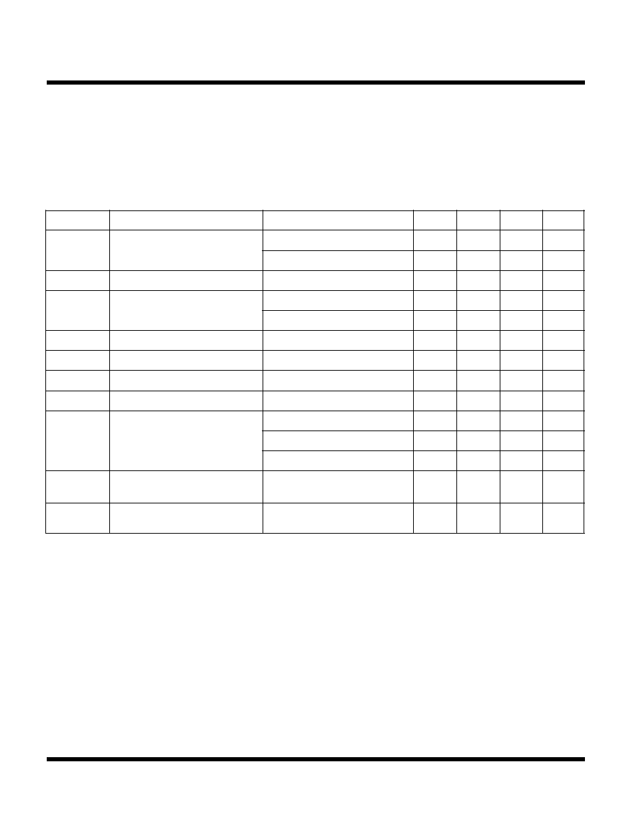
TK116xxU
GND
VIN
VOUT
THERMAL
PROTECTION
BANDGAP
REFERENCE
APPLICATIONS
s
Battery Powered Systems
s
Portable Consumer Equipment
s
Cordless Telephones
s
Personal Communications Equipment
s
Portable Instrumentation
s
Radio Control Systems
s
Toys
s
Low Voltage Systems
FEATURES
s
Low Dropout Voltage
s
Very Low Standby Current (No Load)
s
Good Load Regulation
s
Internal Thermal Shutdown
s
Short Circuit Protection
s
3% Output Voltage Accuracy
s
Customized Versions Are Available
GND
VIN
VOUT
GND
TK116 U
ORDERING INFORMATION
TAPE/REEL CODE
TL: Tape Left
Tape/Reel Code
Voltage Code
VOLTAGE CODE
30 = 3.0 V
33 = 3.3 V
50 = 5.0 V
90 = 9.0 V
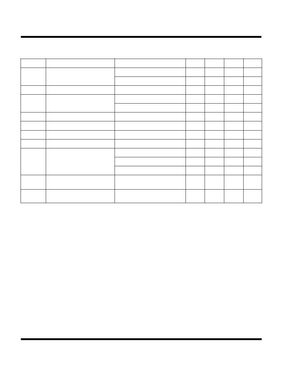
BLOCK DIAGRAM
DESCRIPTION
The TK116xxU series devices are low dropout, linear 3-
terminal regulators.
An internal PNP pass-transistor is used in order to achieve
low dropout voltage (typically 160 mV at 80 mA load
current).
The regulated output voltages of 3, 3.3, 5 and 9 V are
available. The device has very low (400
µ
A) quiescent
current with no load and 2 mA with 60 mA load.
An internal thermal shutdown circuit limits the junction
temperature to below 150
∞
C. The load current is internally
monitored and the device will shut down in the presence
of a short circuit at the output.
The TK116xxU is available in the SOT-89 surface mount
package.
TK116xxU
THREE-TERMINAL VOLTAGE REGULATOR
Page 2
December 1998 TOKO, Inc.
TK116xxU
ABSOLUTE MAXIMUM RATINGS
Supply Voltage ......................................................... 18 V
Operating Voltage Range ............................... 2.5 to 16 V
Load Current ....................................................... 250 mA
Power Dissipation (Note 1) .............................. 1000 mW
Storage Temperature Range ................... -55 to +150
∞
C
Operating Temp. Range (Standard) ............ -30 to +80
∞
C
Lead Soldering Temperature (10 s) ...................... 235
∞
C
Junction Temperature ........................................... 150
∞
C
TK11630U ELECTRICAL CHARACTERISTICS
Test Conditions: T
A
= 25
∞
C, V
IN
= 4.0 V, unless otherwise specified.
Note 1: Power dissipation is 600 mW in free air. Derate at 4.8 mW/
∞
C for operation above 25
∞
C. Power dissipation is 1 W when mounted as
recommended. Derate at 8 mW/
∞
C for operation above 25
∞
C.
Note 2: I
OUT
(Load Current) is current when V
OUT
drops down 0.4 V from V
OUT
at I
OUT
= 10 mA.
Note 3: Refer to "Definition of Terms."
L
O
B
M
Y
S
R
E
T
E
M
A
R
A
P
S
N
O
I
T
I
D
N
O
C
T
S
E
T
N
I
M
P
Y
T
X
A
M
S
T
I
N
U
I
Q
t
n
e
r
r
u
C
t
n
e
c
s
e
i
u
Q
V
N
I
I
,
V
0
.
4
=
T
U
O
A
m
0
=
0
0
4
0
0
8
A
µ
V
N
I
I
,
V
5
.
2
=
T
U
O
A
m
0
=
8
.
0
0
.
2
A
m
V
T
U
O
e
g
a
t
l
o
V
t
u
p
t
u
O
V
N
I
I
,
V
0
.
4
=
T
U
O
A
m
0
1
=
9
.
2
0
.
3
1
.
3
V
V
P
O
R
D
e
g
a
t
l
o
V
t
u
o
p
o
r
D
I
T
U
O
A
m
0
3
=
0
8
0
5
1
A
m
I
T
U
O
A
m
0
0
1
=
0
7
1
0
3
3
V
m
I
T
U
O
t
n
e
r
r
u
C
t
u
p
t
u
O
V
N
I
)
2
e
t
o
N
(
,
V
0
.
4
=
0
9
1
A
m
I
R
O
t
n
e
r
r
u
C
t
u
p
t
u
O
d
e
d
n
e
m
m
o
c
e
R
V
N
I
V
0
.
4
=
0
5
1
A
m
I
D
N
G
)
3
e
t
o
N
(
t
n
e
r
r
u
C
d
n
u
o
r
G
V
N
I
I
,
V
0
.
4
=
T
U
O
A
m
0
6
=
0
.
2
5
.
4
A
m
g
e
R
e
n
i
L
n
o
i
t
a
l
u
g
e
R
e
n
i
L
V
N
I
V
0
.
9
o
t
0
.
4
=
0
.
2
0
3
V
m
g
e
R
d
a
o
L
n
o
i
t
a
l
u
g
e
R
d
a
o
L
V
N
I
I
,
V
0
.
4
=
T
U
O
A
m
0
3
o
t
0
=
5
1
0
6
V
m
V
N
I
I
,
V
0
.
4
=
T
U
O
A
m
0
0
1
o
t
0
=
0
4
0
4
1
V
m
V
N
I
I
,
V
0
.
4
=
T
U
O
A
m
0
5
1
o
t
0
=
0
2
1
0
2
2
V
m
R
R
n
o
i
t
c
e
j
e
R
e
l
p
p
i
R
V
N
I
I
,
V
5
.
4
=
T
U
O
,
A
m
0
1
=
s
m
r
V
m
0
0
1
,
z
H
0
0
4
=
f
5
5
B
d
V
T
U
O
/
T
t
n
e
i
c
i
f
f
e
o
C
e
r
u
t
a
r
e
p
m
e
T
V
N
I
I
,
V
5
.
4
=
T
U
O
,
A
m
0
1
=
C
∞
0
3
-
T
A
C
∞
0
8
+
5
3
.
0
±
C
∞
/
V
m
January 1999 TOKO, Inc.
Page 3
TK116xxU
TK11633U ELECTRICAL CHARACTERISTICS
Test Conditions: T
A
= 25
∞
C, V
IN
= 4.3 V, unless otherwise specified.
Note 1: I
OUT
(Load Current) is current when V
OUT
drops down 0.4 V from V
OUT
at I
OUT
= 10 mA.
Note 2: Refer to "Definition of Terms."
L
O
B
M
Y
S
R
E
T
E
M
A
R
A
P
S
N
O
I
T
I
D
N
O
C
T
S
E
T
N
I
M
P
Y
T
X
A
M
S
T
I
N
U
I
Q
t
n
e
r
r
u
C
t
n
e
c
s
e
i
u
Q
V
N
I
I
,
V
3
.
4
=
T
U
O
A
m
0
=
0
0
4
0
0
8
A
µ
V
N
I
I
,
V
0
.
3
=
T
U
O
A
m
0
=
8
.
0
0
.
2
A
m
V
T
U
O
e
g
a
t
l
o
V
t
u
p
t
u
O
V
N
I
I
,
V
3
.
4
=
T
U
O
A
m
0
1
=
2
.
3
3
.
3
4
.
3
V
V
P
O
R
D
e
g
a
t
l
o
V
t
u
o
p
o
r
D
I
T
U
O
A
m
0
3
=
0
8
0
5
1
A
m
I
T
U
O
A
m
0
0
1
=
0
7
1
0
3
3
V
m
I
T
U
O
t
n
e
r
r
u
C
t
u
p
t
u
O
V
N
I
)
1
e
t
o
N
(
,
V
3
.
4
=
0
9
1
A
m
I
R
O
t
n
e
r
r
u
C
t
u
p
t
u
O
d
e
d
n
e
m
m
o
c
e
R
V
N
I
V
3
.
4
=
0
5
1
A
m
I
D
N
G
)
2
e
t
o
N
(
t
n
e
r
r
u
C
d
n
u
o
r
G
V
N
I
I
,
V
3
.
4
=
T
U
O
A
m
0
6
=
0
.
2
5
.
4
A
m
g
e
R
e
n
i
L
n
o
i
t
a
l
u
g
e
R
e
n
i
L
V
N
I
V
3
.
9
o
t
3
.
4
=
0
.
2
0
3
V
m
g
e
R
d
a
o
L
n
o
i
t
a
l
u
g
e
R
d
a
o
L
V
N
I
I
,
V
3
.
4
=
T
U
O
A
m
0
3
o
t
0
=
5
1
0
6
V
m
V
N
I
I
,
V
3
.
4
=
T
U
O
A
m
0
0
1
o
t
0
=
0
4
0
4
1
V
m
V
N
I
I
,
V
3
.
4
=
T
U
O
A
m
0
5
1
o
t
0
=
0
2
1
0
2
2
V
m
R
R
n
o
i
t
c
e
j
e
R
e
l
p
p
i
R
V
N
I
I
,
V
8
.
4
=
T
U
O
,
A
m
0
1
=
s
m
r
V
m
0
0
1
,
z
H
0
0
4
=
f
5
5
B
d
V
T
U
O
/
T
t
n
e
i
c
i
f
f
e
o
C
e
r
u
t
a
r
e
p
m
e
T
V
N
I
I
,
V
8
.
4
=
T
U
O
,
A
m
0
1
=
C
∞
0
3
-
T
A
C
∞
0
8
+
5
3
.
0
±
C
∞
/
V
m

Page 4
December 1998 TOKO, Inc.
TK116xxU
TK11650U ELECTRICAL CHARACTERISTICS
Test Conditions: T
A
= 25
∞
C, V
IN
= 6.0 V, unless otherwise specified.
Note 1: I
OUT
(Load Current) is current when V
OUT
drops down 0.4 V from V
OUT
at I
OUT
= 10 mA.
Note 2: Refer to "Definition of Terms."
L
O
B
M
Y
S
R
E
T
E
M
A
R
A
P
S
N
O
I
T
I
D
N
O
C
T
S
E
T
N
I
M
P
Y
T
X
A
M
S
T
I
N
U
I
Q
t
n
e
r
r
u
C
t
n
e
c
s
e
i
u
Q
V
N
I
I
,
V
0
.
6
=
T
U
O
A
m
0
=
0
0
4
0
0
8
A
µ
V
N
I
I
,
V
0
.
4
=
T
U
O
A
m
0
=
8
.
0
0
.
2
A
m
V
T
U
O
e
g
a
t
l
o
V
t
u
p
t
u
O
V
N
I
I
,
V
0
.
6
=
T
U
O
A
m
0
1
=
5
8
.
4
0
0
.
5
5
1
.
5
V
V
P
O
R
D
e
g
a
t
l
o
V
t
u
o
p
o
r
D
I
T
U
O
A
m
0
3
=
0
8
0
5
1
A
m
I
T
U
O
A
m
0
0
1
=
0
7
1
0
3
3
V
m
I
T
U
O
t
n
e
r
r
u
C
t
u
p
t
u
O
V
N
I
)
1
e
t
o
N
(
,
V
0
.
6
=
0
9
1
A
m
I
R
O
t
n
e
r
r
u
C
t
u
p
t
u
O
d
e
d
n
e
m
m
o
c
e
R
V
N
I
V
0
.
6
=
0
5
1
A
m
I
D
N
G
)
2
e
t
o
N
(
t
n
e
r
r
u
C
d
n
u
o
r
G
V
N
I
I
,
V
0
.
6
=
T
U
O
A
m
0
6
=
0
.
2
5
.
4
A
m
g
e
R
e
n
i
L
n
o
i
t
a
l
u
g
e
R
e
n
i
L
V
N
I
V
0
.
1
1
o
t
0
.
6
=
0
.
2
0
3
V
m
g
e
R
d
a
o
L
n
o
i
t
a
l
u
g
e
R
d
a
o
L
V
N
I
I
,
V
0
.
6
=
T
U
O
A
m
0
3
o
t
0
=
5
1
0
6
V
m
V
N
I
I
,
V
0
.
6
=
T
U
O
A
m
0
0
1
o
t
0
=
0
4
0
4
1
V
m
V
N
I
I
,
V
0
.
6
=
T
U
O
A
m
0
5
1
o
t
0
=
0
2
1
0
2
2
V
m
R
R
n
o
i
t
c
e
j
e
R
e
l
p
p
i
R
V
N
I
I
,
V
5
.
6
=
T
U
O
,
A
m
0
1
=
s
m
r
V
m
0
0
1
,
z
H
0
0
4
=
f
5
5
B
d
V
T
U
O
/
T
t
n
e
i
c
i
f
f
e
o
C
e
r
u
t
a
r
e
p
m
e
T
V
N
I
I
,
V
5
.
6
=
T
U
O
,
A
m
0
1
=
C
∞
0
3
-
T
A
C
∞
0
8
+
5
3
.
0
±
C
∞
/
V
m
January 1999 TOKO, Inc.
Page 5
TK116xxU
TK11690U ELECTRICAL CHARACTERISTICS
Test Conditions: T
A
= 25
∞
C, V
IN
= 10.0 V, unless otherwise specified.
Note 1: I
OUT
(Load Current) is current when V
OUT
drops down 0.4 V from V
OUT
at I
OUT
= 10 mA.
Note 2: Refer to "Definition of Terms."
L
O
B
M
Y
S
R
E
T
E
M
A
R
A
P
S
N
O
I
T
I
D
N
O
C
T
S
E
T
N
I
M
P
Y
T
X
A
M
S
T
I
N
U
I
Q
t
n
e
r
r
u
C
t
n
e
c
s
e
i
u
Q
V
N
I
I
,
V
0
.
0
1
=
T
U
O
A
m
0
=
0
0
4
0
0
8
A
µ
V
N
I
I
,
V
0
.
8
=
T
U
O
A
m
0
=
8
.
0
0
.
2
A
m
V
T
U
O
e
g
a
t
l
o
V
t
u
p
t
u
O
V
N
I
I
,
V
0
.
0
1
=
T
U
O
A
m
0
1
=
3
7
.
8
0
0
.
9
7
2
.
9
V
V
P
O
R
D
e
g
a
t
l
o
V
t
u
o
p
o
r
D
I
T
U
O
A
m
0
3
=
0
8
0
5
1
A
m
I
T
U
O
A
m
0
0
1
=
0
7
1
0
3
3
V
m
I
T
U
O
t
n
e
r
r
u
C
t
u
p
t
u
O
V
N
I
)
1
e
t
o
N
(
,
V
0
.
0
1
=
0
9
1
A
m
I
R
O
t
n
e
r
r
u
C
t
u
p
t
u
O
d
e
d
n
e
m
m
o
c
e
R
V
N
I
V
0
.
0
1
=
0
5
1
A
m
I
D
N
G
)
2
e
t
o
N
(
t
n
e
r
r
u
C
d
n
u
o
r
G
V
N
I
I
,
V
0
.
0
1
=
T
U
O
A
m
0
6
=
0
.
2
5
.
4
A
m
g
e
R
e
n
i
L
n
o
i
t
a
l
u
g
e
R
e
n
i
L
V
N
I
V
0
.
5
1
o
t
0
.
0
1
=
0
.
2
0
3
V
m
g
e
R
d
a
o
L
n
o
i
t
a
l
u
g
e
R
d
a
o
L
V
N
I
I
,
V
0
.
0
1
=
T
U
O
A
m
0
3
o
t
0
=
5
1
0
6
V
m
V
N
I
I
,
V
0
.
0
1
=
T
U
O
A
m
0
0
1
o
t
0
=
0
4
0
4
1
V
m
V
N
I
I
,
V
0
.
0
1
=
T
U
O
A
m
0
5
1
o
t
0
=
0
2
1
0
2
2
V
m
R
R
n
o
i
t
c
e
j
e
R
e
l
p
p
i
R
V
N
I
I
,
V
5
.
0
1
=
T
U
O
,
A
m
0
1
=
s
m
r
V
m
0
0
1
,
z
H
0
0
4
=
f
5
5
B
d
V
T
U
O
/
T
t
n
e
i
c
i
f
f
e
o
C
e
r
u
t
a
r
e
p
m
e
T
V
N
I
I
,
V
5
.
0
1
=
T
U
O
,
A
m
0
1
=
C
∞
0
3
-
T
A
C
∞
0
8
+
7
.
0
±
C
∞
/
V
m
Page 6
December 1998 TOKO, Inc.
TK116xxU
TYPICAL PERFORMANCE CHARACTERISTICS
T
A
= 25
∞
C, unless otherwise specified.
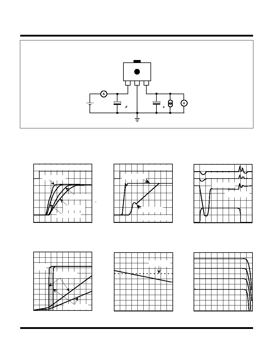
TEST CIRCUIT
10 F
VIN
+
+
+
IIN
CIN
0.1 F
CL
VOUT
IOUT
OUTPUT VOLTAGE RESPONSE
(OFF
ON)
-5
5
25
15
35
CL = 0.33 µF
45
CL = 1.0 µF
CL = 1.5 µF
CL = 0.47 µF
TIME (µs)
ILOAD = 10 mA, CN = 1000 pF
V
OUT
V
CONT
OUTPUT VOLTAGE RESPONSE
(OFF
ON)
0
200
600
TIME (µs)
400
800
CN = 0.01 µF
CN = 0.1 µF
CL = 2.2 µF
ILOAD = 30 mA
V
CONT
V
OUT
LOAD CURRENT STEP RESPONSE
-5
5
15
35
25
45
TIME( µs)
CL = 0.33 µF
V
OUT
(200 mV/DIV)
I LOAD
ILOAD = 5 to 35 mA
30 to 60 mA
0 to 30 mA
CONTROL PIN CURRENT
VS.
VOLTAGE
0
1
2
3
VCONT (V)
0
I CONT
(
µ
A)
10
20
30
40
50
4
5
VOUT
RCONT = 0
RCONT =100K
LOAD REGULATION
0
50
100
IOUT (mA)
V
OUT
(5 mV/DIV)
VOUT(TYP)
SHORT CIRCUIT CURRENT
0
150
300
IOUT (mA)
V
OUT (V)
5
4
3
2
1
0
January 1999 TOKO, Inc.
Page 7
TK116xxU
TYPICAL PERFORMANCE CHARACTERISTICS (CONT.)
T
A
= 25
∞
C, unless otherwise specified.
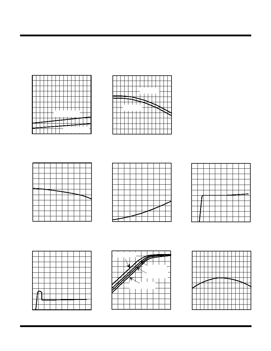
DROPOUT VOLTAGE
VS.
TEMPERATURE
400
200
V
DROP
(
m
V)
500
300
100
TA(
∞
C)
0
IOUT = 80 mA
IOUT = 30 mA
-50 0 50 100
MAXIMUM OUTPUT CURRENT
VS.
TEMPERATURE
I OUT
(mA)
250
200
150
TA(
∞
C)
TK11650
TK11630
-50 0 50 100
OUTPUT VOLTAGE
VS.
OUTPUT CURRENT
IOUT (mA)
V
OUT
(V)
3.1
3.0
2.9
0 50 100
GROUND CURRENT
VS.
OUTPUT CURRENT
IOUT (mA)
I GND
(mA)
10
5
0
0 50 100
OUTPUT VOLTAGE
VS.
INPUT VOLTAGE (1)
VIN (V)
V
OUT
(V)
3.1
3.0
2.9
0 10 20
QUIESCENT CURRENT
VS.
INPUT VOLTAGE
VIN (V)
I Q
(mA)
2
1
0
0 10 20
OUTPUT VOLTAGE
VS.
INPUT VOLTAGE (2)
VIN (V)
V
OUT
(V)
3.0
2.5
2.0
IOUT = 0 mA
IOUT = 30 mA
IOUT = 60 mA
IOUT = 90 mA
2.5 3.0 3.5
OUTPUT VOLTAGE
VS.
TEMPERATURE
TA (
∞
C)
V
OUT
(V)
3.1
3.0
2.9
-50 0 50 100
11630
Page 8
December 1998 TOKO, Inc.
TK116xxU
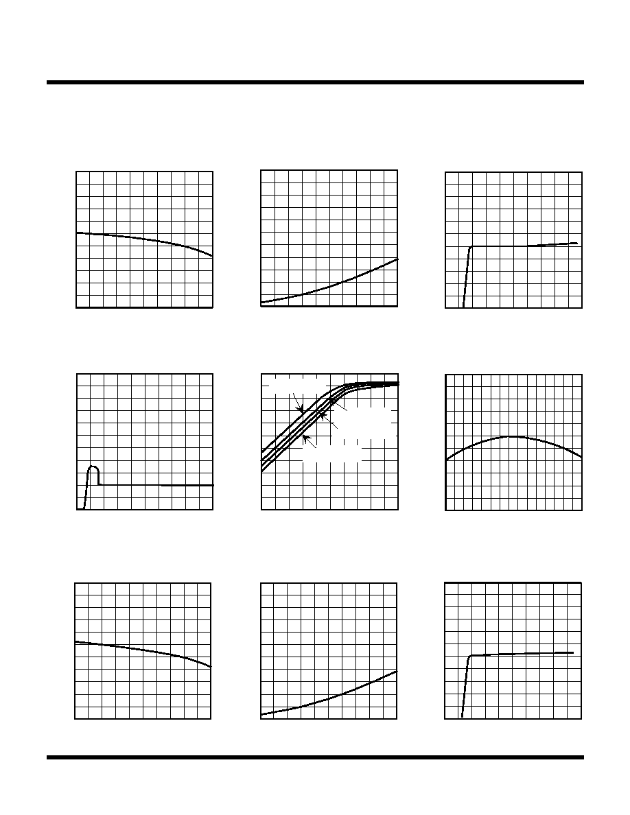
11633
OUTPUT VOLTAGE
VS.
OUTPUT CURRENT
IOUT (mA)
V
OUT
(V)
3.4
3.3
3.2
0 50 100
GROUND CURRENT
VS.
OUTPUT CURRENT
IOUT (mA)
I GND
(mA)
10
5
0
0 50 100
OUTPUT VOLTAGE
VS.
INPUT VOLTAGE (1)
VIN (V)
V
OUT
(V)
3.4
3.3
3.2
0 10 20
QUIESCENT CURRENT
VS.
INPUT VOLTAGE
VIN (V)
I Q
(mA)
2
1
0
0 10 20
OUTPUT VOLTAGE
VS.
INPUT VOLTAGE (2)
VIN (V)
V
OUT
(V)
3.3
2.8
2.3
2.8 3.3 3.8
IOUT = 0 mA
IOUT = 30 mA
IOUT = 60 mA
IOUT = 90 mA
OUTPUT VOLTAGE
VS.
TEMPERATURE
TA (
∞
C)
V
OUT
(V)
3.4
3.3
3.2
-50 0 50 100
OUTPUT VOLTAGE
VS.
OUTPUT CURRENT
IOUT (mA)
V
OUT
(V)
5.1
5.0
4.9
0 50 100
GROUND CURRENT
VS.
OUTPUT CURRENT
IOUT (mA)
I GND
(mA)
10
5
0
0 50 100
OUTPUT VOLTAGE
VS.
INPUT VOLTAGE (1)
VIN (V)
V
OUT
(V)
5.1
5.0
4.9
0 10 20
11650
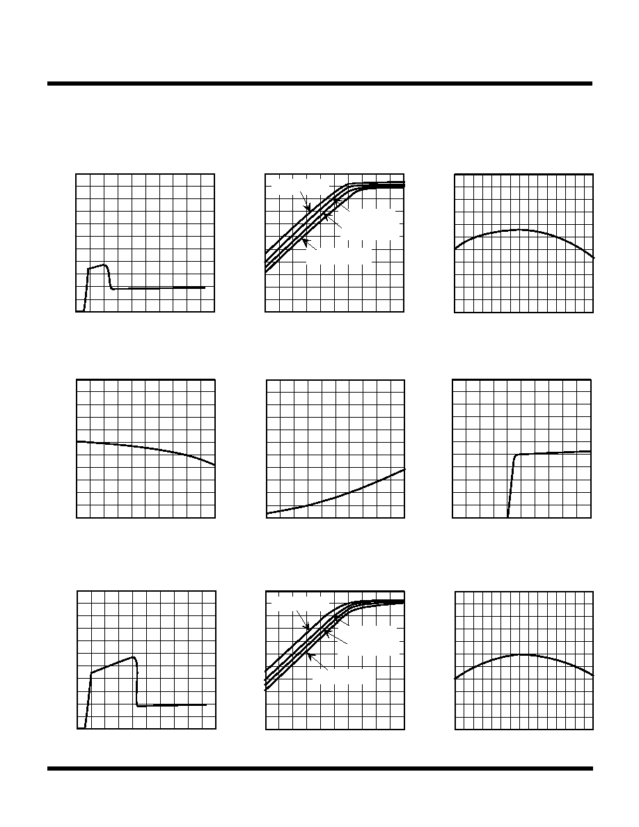
TYPICAL PERFORMANCE CHARACTERISTICS (CONT.)
T
A
= 25
∞
C, unless otherwise specified.
January 1999 TOKO, Inc.
Page 9
TK116xxU
11650 (CONT.)
QUIESCENT CURRENT
VS.
INPUT VOLTAGE
VIN (V)
I Q
(mA)
2
1
0
0 10 20
OUTPUT VOLTAGE
VS.
INPUT VOLTAGE (2)
VIN (V)
V
OUT
(V)
5.0
4.5
4.0
IOUT = 0 mA
IOUT = 30 mA
IOUT = 60 mA
IOUT = 90 mA
4.5 5.0 5.5
OUTPUT VOLTAGE
VS.
TEMPERATURE
TA (
∞
C)
V
OUT
(V)
5.1
5.0
4.9
-50 0 50 100
OUTPUT VOLTAGE
VS.
OUTPUT CURRENT
IOUT (mA)
V
OUT
(V)
9.1
9.0
8.9
0 50 100
GROUND CURRENT
VS.
OUTPUT CURRENT
IOUT (mA)
I GND
(mA)
10
5
0
0 50 100
OUTPUT VOLTAGE
VS.
INPUT VOLTAGE (1)
VIN (V)
V
OUT
(V)
9.1
9.0
8.9
0 10 20
OUTPUT VOLTAGE
VS.
INPUT VOLTAGE (2)
VIN (V)
V
OUT
(V)
9.0
8.5
8.0
IOUT = 0 mA
IOUT = 30 mA
IOUT = 60 mA
IOUT = 90 mA
8.5 9.0 9.5
OUTPUT VOLTAGE
VS.
TEMPERATURE
TA (
∞
C)
V
OUT
(V)
9.1
9.0
8.9
-50 0 50 100
11690
QUIESCENT CURRENT
VS.
INPUT VOLTAGE
VIN (V)
I Q
(mA)
2
1
0
0 10 20
TYPICAL PERFORMANCE CHARACTERISTICS (CONT.)
T
A
= 25
∞
C, unless otherwise specified.

Page 10
December 1998 TOKO, Inc.
TK116xxU
PACKAGE POWER DISSIPATION (P
D
)
This is the power dissipation level at which the thermal
sensor is activated. The IC contains an internal thermal
sensor which monitors the junction temperature. When
the junction temperature exceeds the monitor threshold of
150
∞
C, the IC is shut down. The junction temperature
rises as the difference between the input power (V
IN
x I
IN
)
and the output power (V
OUT
x I
OUT
) increases. The rate of
temperature is greatly affected by the mounting pad
configuration on the PCB, the board material and the
ambient temperature. When the IC mounting has good
thermal conductivity, the junction temperature will be low,
even if the power dissipation is great. When the radiation
of heat is good, the device temperature will be low, even if
the power loss is great. When mounted on the
recommended mounting pad, the power dissipation of the
SOT-89 package is 1000 mW. Derate the power dissipation
at 8 mW/
∞
C for operation above 25
∞
C. To determine the
power dissipation for shutdown when mounted, attach the
device on the actual PCB and deliberately increase the
output current (or raise the input voltage) until the thermal
protection circuit is activated. Calculate the power
dissipation of the device by subtracting the output power
from the input power. The measurements should allow for
the ambient temperature of the PCB. The value obtained
from P
D
/(150
∞
C - T
A
) is the derating factor. The PCB
mounting pad should provide maximum thermal
conductivity in order to maintain low device temperatures.
As a general rule, the lower the temperature, the better the
reliability of the device. The thermal resistance when
mounted is expressed as follows:
T
j
=
jA
x P
D
+ T
A
For Toko ICs, the internal limit for junction temperature is
150
∞
C. If the ambient temperature (T
A
) is 25
∞
C, then:
150
∞
C =
jA
x P
D
+ 25
∞
C
jA
= 125
∞
C/P
D
P
D
is the value when the thermal sensor is activated. A
simple way to determine P
D
is to calculate V
IN
x I
IN
when
the output side is shorted. Input current gradually falls as
temperature rises. You should use the value when the
DEFINITION AND EXPLANATION OF TECHNICAL TERMS
LINE REGULATION (Line Reg)
Line regulation is the ability of the regulator to maintain a
constant output voltage as the input voltage changes. The
line regulation is specified as the input voltage is changed
from V
IN
= V
OUT(TYP)
+ 1 V to V
IN
= V
OUT(TYP)
+ 6 V.
LOAD REGULATION (Load Reg)
Load regulation is the ability of the regulator to maintain a
constant output voltage as the load current changes. It is
a pulsed measurement to minimize temperature effects
with the input voltage set to V
IN
= V
OUT(TYP)
+1 V. The load
regulation is specified under three output current step
conditions of 0 mA to 30 mA, 0 mA to 100 mA and 0 mA to
150 mA.
DROPOUT VOLTAGE (V
DROP
)
This is a measure of how well the regulator performs as the
input voltage decreases. The smaller the number, the
further the input voltage can decrease before regulation
problems occur. Nominal output voltage is first measured
when V
IN
= V
OUT(TYP)
+ 1 V at a chosen load current. When
the output voltage has dropped 100 mV from the nominal,
V
IN
- V
OUT
is the dropout voltage. This voltage is affected
by load current and junction temperature.
GROUND CURRENT (I
GND
)
Ground current is the current which flows through the
ground pin(s). It is defined as I
IN
- I
OUT
, excluding control
current.
OUTPUT NOISE VOLTAGE
This is the effective AC voltage that occurs on the output
voltage under the condition where the input noise is low
and with a given load, filter capacitor, and frequency
range.
THERMAL PROTECTION
This is an internal feature which turns the regulator off
when the junction temperature rises above 150
∞
C. After
the regulator turns off, the temperature drops and the
regulator output turns back on. Under certain conditions,
the output waveform may appear to be an oscillation as the
output turns off and on and back again in succession.
January 1999 TOKO, Inc.
Page 11
TK116xxU
PD
Dpd
25
50
75
150
(mW)
TA (
∞
C)
3
6
5
4
0 50 100 150
TA (
∞
C)
P
D
(mW)
0
600
1000
200
400
800
MOUNTED AS
SHOWN
FREE AIR
DEFINITION AND EXPLANATION OF TECHNICAL TERMS (CONT.)
SOT-89 POWER DISSIPATION CURVE
thermal equilibrium is reached. The range of usable currents
can also be found from the graph below:
Procedure:
1) Find P
D
2) P
D1
is taken to be P
D
x (~ 0.8 - 0.9)
3) Plot P
D1
against 25
∞
C.
4) Connect P
D1
to the point corresponding to the 150
∞
C
with a straight line.
5) In design, take a vertical line from the maximum operating
temperature (e.g., 75
∞
C.) to the derating curve.
6) Read off the value of P
D
against the point at which the
The maximum operating current is:
I
OUT
= (D
PD
/ (V
IN(MAX)
- V
OUT
)
Page 12
December 1998 TOKO, Inc.
TK116xxU
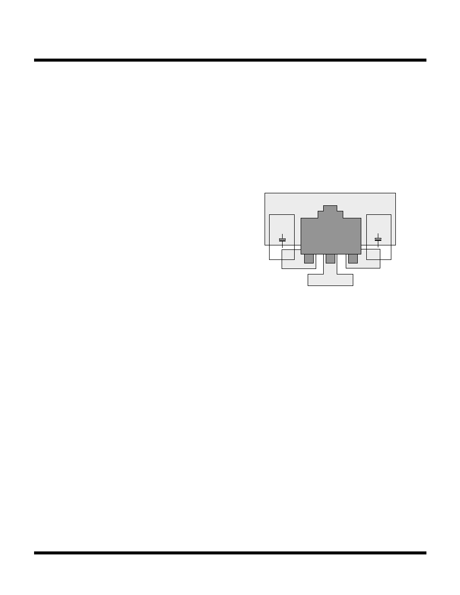
BOARD LAYOUT
Copper pattern should be as large as possible. Power
dissipation is 1000 mW for SOT-89. A low ESR capacitor
is recommended. For low temperature operation, select a
capacitor with a low ESR at the lowest operating
temperature to prevent oscillation, degradation of ripple
rejection and increase in noise. The minimum
recommended capacitance is 2.2
µ
F.
SOT-89 BOARD LAYOUT
APPLICATION INFORMATION
INPUT/OUTPUT DECOUPLING CAPACITOR
CONSIDERATIONS
Voltage regulators require input and output decoupling
capacitors. The required value of these capacitors vary
with application. Capacitors made by different
manufacturers can have different characteristics,
particularly with regard to high frequencies and Equivalent
Series Resistance (ESR) over temperature. The type of
capacitor is also important. For example, a 4.7
µ
F aluminum
electrolytic may be required for a certain application. If a
tantalum capacitor is used, a lower value of 2.2
µ
F would
be adequate. It is important to consider the temperature
characteristics of the decoupling capacitors. While Toko
regulators are designed to operate as low as -30
∞
C, many
capacitors will not operate properly at this temperature.
The capacitance of aluminum electrolytic capacitors may
decrease to 0 at low temperatures. This may cause
oscillation on the output of the regulator since some
capacitance is required to guarantee stability. Thus, it is
important to consider the characteristics of the capacitor
over temperature when selection decoupling capacitors.
The ESR is another important parameter. The ESR will
increase with temperature but low ESR capacitors are
often larger and more costly. In general, tantalum capacitors
offer lower ESR than aluminum electrolytic, but new low
ESR aluminum electrolytic capacitors are now available
from several manufacturers. Usually a bench test is
sufficient to determine the minimum capacitance required
for a particular application. After taking thermal
characteristics and tolerance into account, the minimum
capacitance value should be approximately two times this
value. Please note that linear regulators with a low dropout
voltage have high internal loop gains which require care in
guarding against oscillation caused by insufficient
decoupling capacitance. The use of high quality decoupling
capacitors suited for your application will guarantee proper
operation of the circuit.
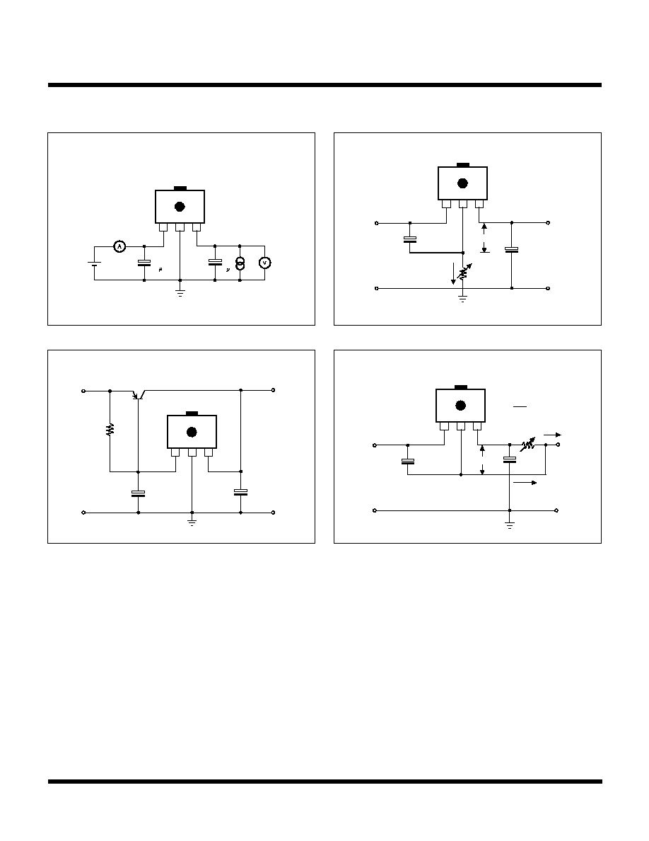
+
VOUT
+
VIN
GND
January 1999 TOKO, Inc.
Page 13
TK116xxU
4.7 µF
VIN
+
+
IN
1 µF
OUT
OUT
VOUT
R
IOUT = + IQ
VOUT
R
GND
IQ
IOUT
VOLTAGE REGULATOR CIRCUIT
VOLTAGE BOOST CIRCUIT
CURRENT BOOST CIRCUIT
CURRENT REGULATOR CIRCUIT
APPLICATION NOTES
Maximize copper foil area connecting to all IC pins for optimum heat conduction. Place input and output bypass capacitors
close to the GND pin.
For best transient behavior and lowest output impedance, use as large a capacitor value as possible. The temperature
coefficient of the capacitance and Equivalent Series Resistance (ESR) should be taken into account. These parameters
can influence power supply noise and ripple rejection. In extreme cases, oscillation may occur. In order to maintain
stability, the output bypass capacitor value should be minimum 1
µ
F for tantalum electrolytic or 4.7
µ
F for aluminum
electrolytic at T
A
= 25
∞
C.
TYPICAL APPLICATIONS
10 F
VIN
+
+
+
IIN
CIN
0.1 F
CL
VOUT
IOUT
4.7 µF
VIN
+
+
IN
1 µF
VO
OUT
VOUT
IQ
R
VO = VOUT + IQ X R
GND
GND
4.7 µF
VIN
+
+
IN
10 µF
VOUT
OUT
100
Page 14
December 1998 TOKO, Inc.
TK116xxU
0.48 max
0.53 max
0.48 max
1.5
1.5
3.0
e'
4.5
1.8 max
0.4
2.5
0.8 max
4.25 max
1
2
3
e
e
Product Code
Marking
+ 0.1
+ 0.1
0.44 max
0.44 max
1.5
1.0
1.0
1.0
3.0
0.7
1.5
1.5
1.5
45
∞
Recommended Mount Pad
2.0
e
e
Dimensions are shown in millimeters
Tolerance: x.x =
±
0.2 mm (unless otherwise specified)
+ 0.1
Marking Information
Product Code
A
Voltage Code
TK11630U
30
TK11633U
33
TK11650U
50
TK11690U
90
SOT-89 (SOT-89-3)
PACKAGE OUTLINE
Printed in the USA
© 1999 Toko, Inc.
All Rights Reserved
TOKO AMERICA REGIONAL OFFICES
Toko America, Inc. Headquarters
1250 Feehanville Drive, Mount Prospect, Illinois 60056
Tel: (847) 297-0070 Fax: (847) 699-7864
IC-115-TK116U
0798O0.0K
Visit our Internet site at http://www.tokoam.com
The information furnished by TOKO, Inc. is believed to be accurate and reliable. However, TOKO reserves the right to make changes or improvements in the design, specification or manufacture of its
products without further notice. TOKO does not assume any liability arising from the application or use of any product or circuit described herein, nor for any infringements of patents or other rights of
third parties which may result from the use of its products. No license is granted by implication or otherwise under any patent or patent rights of TOKO, Inc.
Western Regional Office
Toko America, Inc.
2480 North First Street , Suite 260
San Jose, CA 95131
Tel: (408) 432-8281
Fax: (408) 943-9790
Midwest Regional Office
Toko America, Inc.
1250 Feehanville Drive
Mount Prospect, IL 60056
Tel: (847) 297-0070
Fax: (847) 699-7864
Eastern Regional Office
Toko America, Inc.
107 Mill Plain Road
Danbury, CT 06811
Tel: (203) 748-6871
Fax: (203) 797-1223
Semiconductor Technical Support
Toko Design Center
4755 Forge Road
Colorado Springs, CO 80907
Tel: (719) 528-2200
Fax: (719) 528-2375