
Page 1 of 17 TOPRO CONFIDNETIAL 2003/7/31
Print
TP 6820
Digital Camera Solution
(QQVGA/RS232/turn-key solution)
D
D
D
a
a
a
t
t
t
a
a
a
S
S
S
h
h
h
e
e
e
e
e
e
t
t
t
Version: 1.0
April/2002
http://www.topro.com.tw
HQ:
5 F, No.10, Prosperity Road 1, Science-Based Industrial Park, Hsinchu 300, Taiwan, R.O.C
300 10 5
TPE:
5 F, No.27, Min Chuan W. Rd. Taipei 104, Taiwan, R.O.C
104 27 5
SHENZHEN
:
Room 802, Tower A, World Trade Plaza, Fahong Rd., Fatian, Shenzhen, China
9 A 802 (518033)
H.Q.: Tel: 886-3-5632515 Fax: 886-3-5641728
TPE. Tel: 886-2-25856858 Fax:886-2-25941104
SHENZHEN: TEL: 755-3679985 Fax: 755-3679518

Page 2 of 17 TOPRO CONFIDNETIAL 2003/7/31
Print
TP 6820
Digital Camera Solution
(QQVGA/RS232/turn-key solution)
G
G
e
e
n
n
e
e
r
r
a
a
l
l
S
S
p
p
e
e
c
c
i
i
f
f
i
i
c
c
a
a
t
t
i
i
o
o
n
n
G
G
e
e
n
n
e
e
r
r
a
a
l
l
D
D
e
e
s
s
c
c
r
r
i
i
p
p
t
t
i
i
o
o
n
n
The TP6820, when collocated with PAS009 CMOS image sensor made by Pixart, provides a
total solution for a QQVGA resolution RS232 interface digital camera. It can act as a digital
still camera when stand-alone mode, it also can act as a live view camera when connecting to
PC through RS232 interface. By adding a SRAM with 128kx8 bits capacity, it can store
twelve pictures while snapshot button is pressed. When connecting to PC, user can get the
images from this storage through RS232 with "Show Me Cam " software application.
F
F
e
e
a
a
t
t
u
u
r
r
e
e
Supports PAS 009 sensor interface
Supports Image processor.
Supports Image snapshot function.
Supports auto power saving mode with port wake up function
Supports RS232 interface, up to 115200bps speed.
Supports indicator LED.
Supports warning buzzer
Supports H/W erase picture function.
Embedded an 8-bits (80C51) micro controller.
Embedded 128 bytes of RAM
Embedded 4K bytes of ROM
Support wide supply voltage range: from 3.0V to 3.6V
Operating frequency : 11.0592MHz
Support SRAM interface with 128 Kbytes capacity
C
C
a
a
m
m
e
e
r
r
a
a
S
S
p
p
e
e
c
c
i
i
f
f
i
i
c
c
a
a
t
t
i
i
o
o
n
n
s
s
:
:
Sensor: QQ VGA color CMOS sensor. (PAS 009)
Resolution: 160x120
Storage: 12 pictures stores.

Page 3 of 17 TOPRO CONFIDNETIAL 2003/7/31
Print
TP 6820
Digital Camera Solution
(QQVGA/RS232/turn-key solution)
Interface: RS232.
Indicator: LED and Buzzer.
Battery: AA x3
Power Life:
20,000 pictures snap at operation mode
Suspend current <10uA
Supports self-timer.
A
A
p
p
p
p
l
l
i
i
c
c
a
a
t
t
i
i
o
o
n
n
s
s
Toy camera

Page 4 of 17 TOPRO CONFIDNETIAL 2003/7/31
Print
TP 6820
Digital Camera Solution
(QQVGA/RS232/turn-key solution)
Contents
1. General Specification
P. 2 ---
P.
3
2. Pin Configurations and Package Type
P. 5 ---
P.
6
3. Pin Descriptions
P. 7 ---
P.
7
4. Functional Block Diagram
P. 8 ---
P.
8
5. Function Descriptions
P. 9 ---
P.
11
6. Absolute Maximum Ratings
P. 12 ---
P.
12
7. DC Electrical Characteristic
P. 13 ---
P.
13
8. AC Electrical Characteristic
P. 14 ---
P.
14
9. Application Diagrams
P. 15 ---
P.
17

Page 5 of 17 TOPRO CONFIDNETIAL 2003/7/31
Print
TP 6820
Digital Camera Solution
(QQVGA/RS232/turn-key solution)
P
P
i
i
n
n
C
C
o
o
n
n
f
f
i
i
g
g
u
u
r
r
a
a
t
t
i
i
o
o
n
n
s
s
a
a
n
n
d
d
P
P
a
a
c
c
k
k
a
a
g
g
e
e
T
T
y
y
p
p
e
e
:
:
4
4
0
0
C
C
O
O
B
B
Pin NO.
X , Y
Pin NO.
X , Y
Pin1: GND
-55.000, 645.000 Pin21: P1_PAD2
53.550, -645.000
Pin2: P3_PAD5
-164.950, 645.000 Pin22: P1_PAD3
163.550, -645.000
Pin3: P3_PAD7
-274.950, 645.000 Pin23: P1_PAD4
273.550, -645.000
Pin4: P3_PAD6
-384.950, 645.000 Pin24: P1_PAD5
383.550, -645.000
Pin5: P3_PAD0
-494.950, 645.000 Pin25: P1_PAD6
493.550, -645.000
Pin6: P3_PAD1
-653.700, 457.300 Pin26: P1_PAD7
603.550, -645.000
Pin7: P3_PAD2
-653.700, 347.300 Pin27: P2_PAD0
653.700, -422.700
Pin8: P3_PAD3
-653.700, 237.300 Pin28: P2_PAD1
653.700, -312.700
Pin9: P3_PAD4
-653.700, 127.300 Pin29: P2_PAD2
653.700, -202.700
Pin10: RESET
-653.700, 17.250 Pin30: P2_PAD3
653.700, -92.700
Pin11: P0_PAD0 -653.700, -92.700 Pin31: P2_PAD4
653.700, 17.300
Pin12: P0_PAD1 -653.700, -202.700 Pin32: P2_PAD5
653.700, 127.300
Pin13: P0_PAD2 -653.700, -312.700 Pin33: P2_PAD6
653.700, 237.300
Pin14: P0_PAD3 -653.700, -422.700 Pin34: P2_PAD7
653.700, 347.300
Pin15: P0_PAD4 -653.700, -532.700 Pin35: OUTPUT0 653.700, 457.300
Pin16: P0_PAD5 -496.450, -645.000 Pin36: OUTPUT1 653.700, 567.200
Pin17: P0_PAD6 -386.450, -645.000 Pin37: OUTPUT2 385.050, 645.000
Pin18: P0_PAD7 -276.450, -645.000 Pin38: VDD
275.000, 645.000
Pin19: P1_PAD0 -166.450, -645.000 Pin39: OSCI
165.000, 645.000
Pin20: P1_PAD1 -56.450, -645.000 Pin40: OSCO
55.000, 645.000
Page 6 of 17 TOPRO CONFIDNETIAL 2003/7/31
Print
TP 6820
Digital Camera Solution
(QQVGA/RS232/turn-key solution)

Page 7 of 17 TOPRO CONFIDNETIAL 2003/7/31
Print
TP 6820
Digital Camera Solution
(QQVGA/RS232/turn-key solution)
P
P
i
i
n
n
D
D
e
e
s
s
c
c
r
r
i
i
p
p
t
t
i
i
o
o
n
n
s
s
SYMBOL MODE
FUNCTION
DESCRIPTION
VSS
I
Circuit GND Potential.
VCC
I
Main Power Supply(+4.5V~+5.5V)
RST I
A low level input resets the CPU. A small internal pull-up resistor
permits power-on reset using only a capacitor connected to GND.
ADD0~ADD16
I/O
Address pins for sram and sensor
DATA0~7
I/O
Connect to data pins of sram and sensor
RX
I
Receive data from pc through RS232 serial interface
TX
O
Transfer data to pc through RS232 serial interface
CS
O
Control PAS009 sensor
EOF
I
Control PAS009 sensor
WR_HALT
O
Control PAS009 sensor
RAM_WR
O
Control sram to read or write
SNAP
I
A low level input will active to snap an image
LED
O
Direct output, connect to a LED
BUZZER
O
Direct output, connect to a buzzer
CS_RAM
O
Direct output, connect to memory chip select CS1.
OSCI
I
Input to inverting oscillator amplifier
OSCO
O
Oscillator output pin
Note: "I" means INPUT function; "O" means OUTPUT function.
Page 8 of 17 TOPRO CONFIDNETIAL 2003/7/31
Print
TP 6820
Digital Camera Solution
(QQVGA/RS232/turn-key solution)
F
F
u
u
n
n
c
c
t
t
i
i
o
o
n
n
a
a
l
l
B
B
l
l
o
o
c
c
k
k
D
D
i
i
a
a
g
g
r
r
a
a
m
m
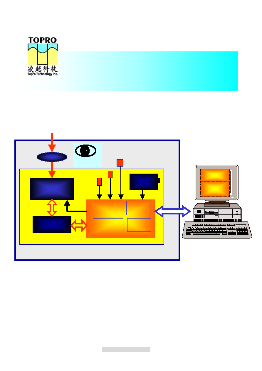
RS232
CMOS sensor
PAS 009A
SRAM 128x8
TP 6820
80C5
1
ROM
Snap Key
LED
Buzzer
Viewfind
LENS
Camera
Camera EE
Sensor IF
Battery
Image
Process
or
Color
Processing
Driver
Application

Page 9 of 17 TOPRO CONFIDNETIAL 2003/7/31
Print
TP 6820
Digital Camera Solution
(QQVGA/RS232/turn-key solution)
F
F
u
u
n
n
c
c
t
t
i
i
o
o
n
n
D
D
e
e
s
s
c
c
r
r
i
i
p
p
t
t
i
i
o
o
n
n
s
s
S
S
R
R
A
A
M
M
i
i
n
n
t
t
e
e
r
r
f
f
a
a
c
c
e
e
TP6820
can support a SRAM up to 128Kbytes. It can store twelve pictures with 160x120
resolution. By pressing once snapshot button, one picture is stored.
A
A
u
u
t
t
o
o
p
p
o
o
w
w
e
e
r
r
s
s
a
a
v
v
e
e
TP6820
also has auto-power-save mode. If it doesn't be used for 10 seconds,
TP6820
will
change to power save mode and also control the external SRAM and CMOS sensor to power
save mode. By receiving any command from PC or pressing snapshot button, it can be waked
up and continue to work.
C
C
a
a
m
m
e
e
r
r
a
a
a
a
t
t
P
P
o
o
r
r
t
t
a
a
b
b
l
l
e
e
m
m
o
o
d
d
e
e
When camera at portable mode (stand-alone), it acts as a DSC and supports 4 functions: take a
picture, erase all pictures, self-timer, and real time wake up.
Take a picture:
user can take a picture by pressing SNAP- key
ERASE all pictures:
user can erase all pictures by pressing SNAP- key and hold more
than 6 sec
Self-timer:
TP 6820
will enable auto power saving function to enter suspend mode
after 10 sec idle.
Real-time wake up:
TP 6820
will enable camera from suspend mode
C
C
a
a
m
m
e
e
r
r
a
a
a
a
t
t
O
O
n
n
-
-
L
L
i
i
n
n
e
e
m
m
o
o
d
d
e
e
When connecting to PC through RS232 interface, camera is at on-line mode and can act as a
live view camera controlled by either host or camera itself.
Host Control
One Click to
see live pictures
in Monitor.
One Click to
take a picture
, picture stored in host working area.

Page 10 of 17 TOPRO CONFIDNETIAL 2003/7/31
Print
TP 6820
Digital Camera Solution
(QQVGA/RS232/turn-key solution)
One Click to
take 12concecutive pictures,
picture stored in host working area.
One Click to
connect camera and transfer pictures
from camera device to host
working area. .
One Click to
erase all pictures
in camera device
Device Control
Press snap key to take a picture
, picture stored in camera device.
Press snap key more than 6 sec to erase all picture
in camera device.
I
I
n
n
d
d
i
i
c
c
a
a
t
t
o
o
r
r
(
(
L
L
E
E
D
D
&
&
B
B
u
u
z
z
z
z
e
e
r
r
)
)
D
D
e
e
s
s
c
c
r
r
i
i
p
p
t
t
i
i
o
o
n
n
s
s
Two external components, LED and buzzer, should show the status of camera by will work at
the same time to device when the snapshot button pressed. Its relationship is showed below.
Camera @Portable Mode BUZZER
LED
SNAP Mode: press SNAP �KEY to take a picture
Effective SNAP: Take a
picture
One Beep
ON when SNAP processing
OFF when SNAP done
LAST SNAP: Take a picture
and indicate memory full
One Beep to SNAP
One long Beep to indicate
memory full
ON when SNAP processing
OFF when SNAP done
ON-OFF again to indicate
memory full
Memory FULL SNAP: Not
take a picture
3 Short BEEP
3 FLASH
Invalid SNAP: SNAP during
camera busy, not take a
picture.
No action
No extra action
ERASE Mode: press SNAP �KEY and hold more than 6 sec to erase all pictures
Effective ERASE: One Long BEEP in the end to indicate all pictures erased. (There are 3
process when press SNAP-KEY and hold, in the beginning is SNAP function, then warning
occurred when hold over 3 sec. Finally One Long BEEP to indicate all pictures erased.)
SNAP
The same as SNAP mode
The same as SNAP mode
Warning when SNAP-KEY
hold over 3 sec
9 Short BEEPS
9 FLASH
Memory EMPTY
One Long BEEP to indicate
One Long ON-OFF to

Page 11 of 17 TOPRO CONFIDNETIAL 2003/7/31
Print
TP 6820
Digital Camera Solution
(QQVGA/RS232/turn-key solution)
memory empty.
indicate memory empty.
Invalid ERASE: If SNAP-KEY not holds over 6 sec, that is to say, One Long BEEP not
occurred, all the pictures still stored in camera device.

Page 12 of 17 TOPRO CONFIDNETIAL 2003/7/31
Print
TP 6820
Digital Camera Solution
(QQVGA/RS232/turn-key solution)
A
A
b
b
s
s
o
o
l
l
u
u
t
t
e
e
M
M
a
a
x
x
i
i
m
m
u
u
m
m
R
R
a
a
t
t
i
i
n
n
g
g
s
s
Parameter Rating
Unit
Operating Temperature
0+70
Storage Temperature
-65+150
Voltage on Any Pin
-0.5+7
V
Power Dissipation
0.2
W
Note: Stresses above those listed may cause permanent damage to the device. Exposure to
absolute maximum rating conditions for extended periods may affect device reliability.

Page 13 of 17 TOPRO CONFIDNETIAL 2003/7/31
Print
TP 6820
Digital Camera Solution
(QQVGA/RS232/turn-key solution)
D
D
C
C
E
E
l
l
e
e
c
c
t
t
r
r
i
i
c
c
a
a
l
l
C
C
h
h
a
a
r
r
a
a
c
c
t
t
e
e
r
r
i
i
s
s
t
t
i
i
c
c
(TA=0
0
C-70
0
C,VCC=5�10%,VSS=0V)
Limit
Parameter Symbol
Min typ
Max
Unit Test
condition
Input Low Voltage
VIL
-0.5
0.2VCC-0.
1
V
Input High Voltage (Except XTAL1,
RST, P3.0~P3.2)
VIH
0.2VCC
+0.9
VCC+0.5
V
Input High Voltage (XTAL1, RST)
VIH1
0.9VCC
VCC+0.5
V
Input High Voltage (P3.0~P3.2)
VIH2
0.2
VCC
+2.5
VCC+0.5
V
Output Low Voltage
(Except P3.0~P3.2, LED0~2)
VOL
0.45 V
IOL=1.6mA
Output Low Voltage (P3.0~P3.2,
LED0~2)
V OL1
0.7 V
IOL=1.6mA
Output High Voltage
VOH
2.4
V IOH=-60A
Input Leakage Current
(Except P3.6, P3.7)
IIL
-50 A
Vin=0.45V
Input Leakage Current (Port0)
IIL1
10 A
Vin= VCC
Input Leakage Current (P3.6, P3.7)
IIL2
-350 A
Vin=0.45V
Power Supply Current
ICC
15
30 mA
FOP=20MH
z
Idle Mode Supply Current
IID
1.7 5 mA
Power Down Mode Supply Current IPD
5
50
A
Capacitance of I/O Buffer
CIO
10 pF
FOP=1MHz
Internal Reset Pull-Up Resistor
RRST 50
150 K
Notes: (1) All DC electrical characteristics are measured at 25.
(2) It is suggested that conventional precautions should be taken to avoid applying
voltages greater than the absolute maximum ratings.
Page 14 of 17 TOPRO CONFIDNETIAL 2003/7/31
Print
TP 6820
Digital Camera Solution
(QQVGA/RS232/turn-key solution)
A
A
C
C
E
E
l
l
e
e
c
c
t
t
r
r
i
i
c
c
a
a
l
l
C
C
h
h
a
a
r
r
a
a
c
c
t
t
e
e
r
r
i
i
s
s
t
t
i
i
c
c
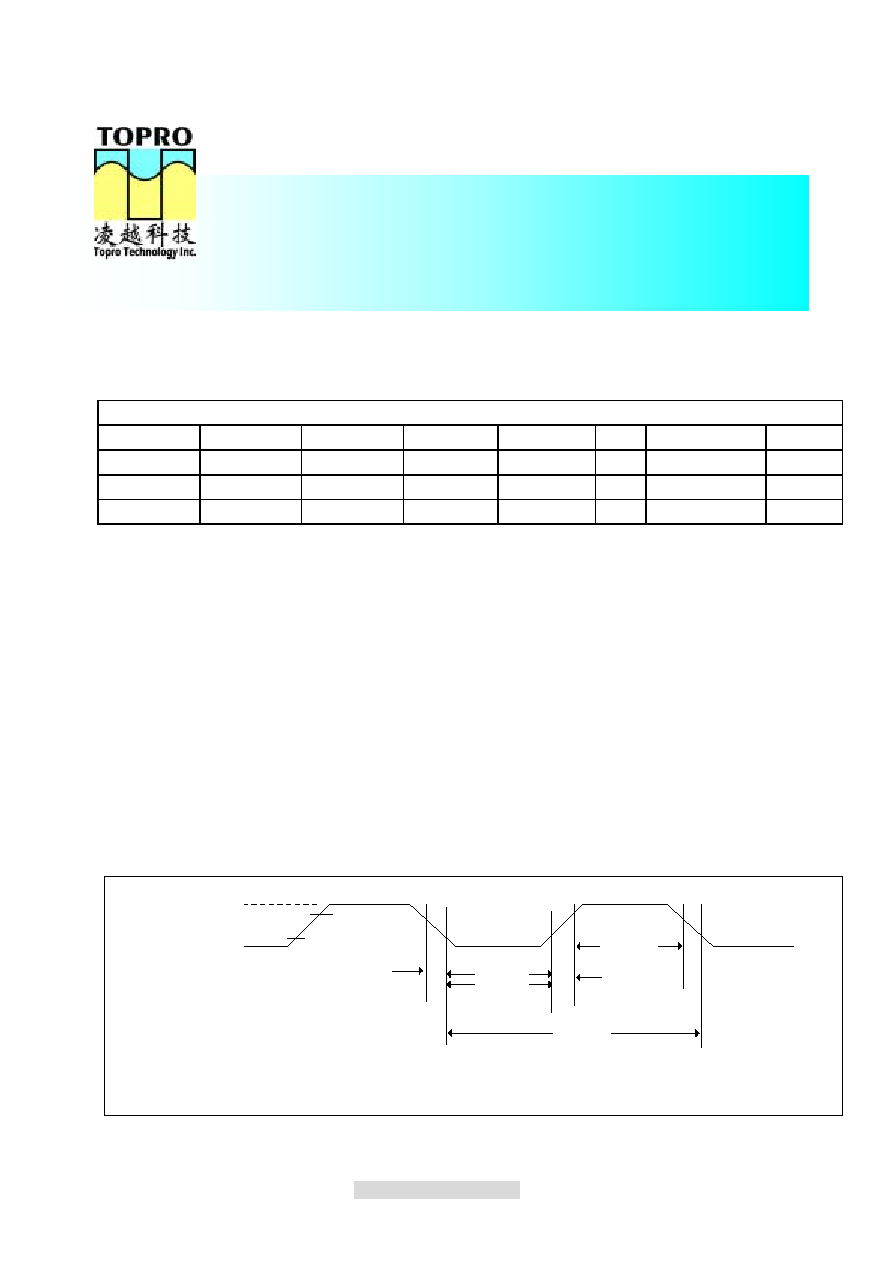
TA=0 to +70,or TA=-40 to +85/+125,VCC=5V�10%,VSS=0V
1
External Clock
TCHCX
5
High time2
20
20
tCLCL-tLOW
ns
TCLCX
5
Low time2
20
20
tCLCL-tHIGH
ns
TCLCH
5
Rise time2
20
10 ns
TCHCL
5
Fall time2
20
10 ns
Notes:1. Parameters are valid over operating temperature range unless otherwise specified.
2. These values are characterized but not 100% production tested.
EXPLANATION OF THE AC SYMBOLS
Each timing symbol has five characters. The first character is always "t"(=time). The other characters, depending on
their positions, indicate the name of a signal or the logical status of that signal. The designations are:
C - Clock
H - Logic level high
L - Logic level low
t - Time
X - No longer a valid logic level
VCC-0.5
0.45V
0.7Vcc
0.2V cc
t CHCL
t CLCX
t
CHCX
t CLCL
t CLCH
Figure 3. External Clock Drive

Page 15 of 17 TOPRO CONFIDNETIAL 2003/7/31
Print
TP 6820
Digital Camera Solution
(QQVGA/RS232/turn-key solution)
A
A
p
p
p
p
l
l
i
i
c
c
a
a
t
t
i
i
o
o
n
n
D
D
i
i
a
a
g
g
r
r
a
a
m
m
s
s
A
A
p
p
p
p
l
l
i
i
c
c
a
a
t
t
i
i
o
o
n
n
c
c
i
i
r
r
c
c
u
u
i
i
t
t
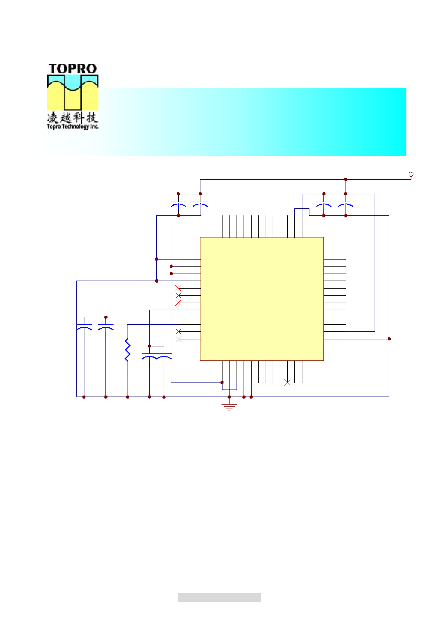
Page 16 of 17 TOPRO CONFIDNETIAL 2003/7/31
Print
TP 6820
Digital Camera Solution
(QQVGA/RS232/turn-key solution)
C4
22PF
C5
22PF
VCC
P00
P01
P02
P03
P04
P05
P06
P07
P20 P21
P22
P23
P24
P25
P26
P27
P10
P11
P12
P13
P14
P15
P17
P16
CRYSTAL
11.0592MHZ
VCC
DGND
P00
P01
P02
P03
P04
P05
P06
P07
P20
P21
P22
P23
P24
P25
P26
P10
P11
P12
P13
WRI
T
E
WRITE
EOF
WR_HAL
T
C17
0.1UF
VCC
P14
P15
P16
P17
P27
P34
P34
2
2
3
3
4
4
1
1
S1
SNAP
Q2
2N3906
Q1
2N3904
R4
10K
R5
4.7K
R6
47K
R7
47K
TXD
RXD
VCC
CS_RAM
VSS
1
WR_HAL
T
2
TX
3
RX
4
RAM_WR
5
CS
6
EOF
7
SNAP
8
ADD16
9
RS
T
10
ADD0
11
ADD1
12
ADD2
13
ADD3
14
ADD4
15
ADD5
16
ADD6
17
ADD7
18
DATA0
19
DATA1
20
DATA2
21
DATA3
22
DATA4
23
DATA5
24
DATA6
25
DATA7
26
ADD8
27
ADD9
28
ADD10
29
ADD11
30
ADD12
31
ADD13
32
ADD14
33
ADD15
34
LED
35
BUZZER
36
CS_RAM
37
VCC
38
OSCI
39
OSCO
40
TP6820
U1
TP6820
RX TX
CS
CS_RAM
1
2
3
RS232
A14
11
A12
12
A7
13
A6
14
A5
15
A4
16
A3
17
A2
18
A1
19
A0
20
IO1
21
IO2
22
IO3
23
VSS
24
IO4
25
IO5
26
IO6
27
IO7
28
IO8
29
CS1
30
A10
31
OE
32
A11
1
A9
2
A8
3
A13
4
WE
5
CS2
6
A15
7
VDD
8
A16
10
U2
B1
BUZZER
D1
LED
VCC
VCC
1
2
POWER
C2
0.1uf
C3
1uf
C1
0.1uf
L1
beat
L2
beat
Page 17 of 17 TOPRO CONFIDNETIAL 2003/7/31
Print
TP 6820
Digital Camera Solution
(QQVGA/RS232/turn-key solution)
A0
1
A1
2
A2
3
A3
4
A4
5
A5
6
DVDD2
7
DGND2
8
A6
9
A7
10
A8
11
A9
12
A10
13
A11
14
A12
15
A13
16
A14/
D7
17
D6
18
GNDD
19
VHRST
20
AVDD1
21
AGND1
22
NC2
23
TEST_SP1
24
TEST_SP2
25
V1V
26
VCM
27
ROSC
28
TEST_PA1
29
TEST_PA2
30
AVDD2
31
AGND2
32
MODE
33
GND1
34
GND2
35
CS
36
WR_HALT
37
WEB
38
EOF
39
PCLK
40
HS
41
VS
42
DGND1
43
DVDD1
44
D3
45
D2
46
D1
47
D0
48
PAS009
U3
PAS009A
P10
P11
P12
P13
P00
P01
P02
P03
P04
P05
P06
P07
P20
P21
P22
P23
P24
P25
C9
0.1u
C10
4.7u
C11
0.1u
C12
4.7u
C13
10u
C14
0.1u
C15
10u
C16
0.1u
R3
33K
VCC
EOF
CS
WR_HALT WRITE
P17
P14
P15
P16