Negative Voltage Regulators
Series
359
3
Negative Voltage Regulators
Series
General Description
Features
Applications
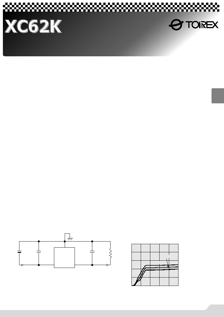
Typical Application Circuit
Typical Performance
Characteristic
The XC62K series are highly precise, low power consumption, negative
voltage regulators, manufactured using CMOS and laser trimming
technologies. The series achieves high output currents with small input-
output voltage differentials, and consists of a high precision voltage
reference, an error correction circuit, and an output driver with current
limitation.
SOT-23 (150mW), SOT-89 (500mW) and TO-92 (300mW) packages are
available.
Ultra Small Input-Output Voltage Differential
: 50mA output possible with a 0.12V
differential (V
OUT
=-5.0V).
Maximum Output Current : 100mA (within max. power
dissipation, V
OUT
= -5.0V)
Output Voltage Range
: -2.1V ~ -6.0V in 0.1V increments.
-5.0, -4.0, -3.0V, -2.5V standard.
(All other voltages are semi-custom)
Highly Accurate
: Output voltage ±2%
(±1% for semi-custom products)
Low Power Consumption : Typ. 3.0
µA @ V
OUT
= -5.0V
Output Voltage Temperature Characteristics
: Typ. ±100ppm/∞C
Input Stability
: Typ. 0.1%/V
Ultra Small Packages
: SOT- 23 (150mW) mini-mold,
SOT-89 (500mW) mini-power mold
TO-92 (300mW)
GBattery Powered Equipment
GPortable & Cellular Phones
GVarious Portable Equipment
GPower Supply for GaAs Applications
NCMOS Low Power Consumption
NSmall Input-Output Voltage Differential
: 0.12V @ 50mA,
0.38V @ 100mA
NMaximum Output Current: 100mA (V
OUT
=-5.0V)
NHighly Accurate
: ±2% (±1%)
NOutput Voltage Range : -2.1V~ -6.0V
NSupply Current
: 3.0
µA (V
OUT
=-5.0V)
NSOT-23/SOT-89/TO-92 Package
+
+
-V
OUT
-V
IN
V
SS
IN
C
IN
C
L
OUT
1
µF
Tantalum
1
µF
Tantalum
0
2
3
4
5
0
-6
-10
Supply Current:Iss
µ
A
Input Voltage:V
IN
V
XC62KN3002-3.0V
-4
-8
-2
Topr25
80
-30
1
03S_10XC62K 02.9.12 3:08 PM 359
XC62K
Series
360
3
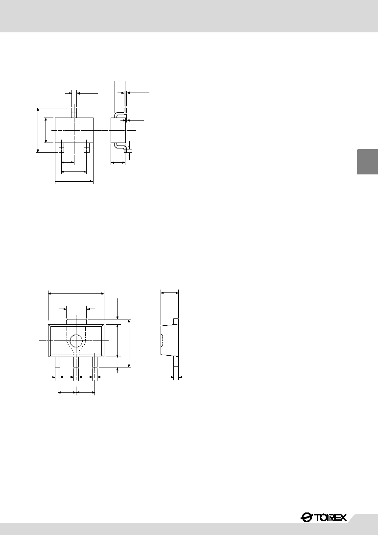
Pin Configuration
Pin Assignment
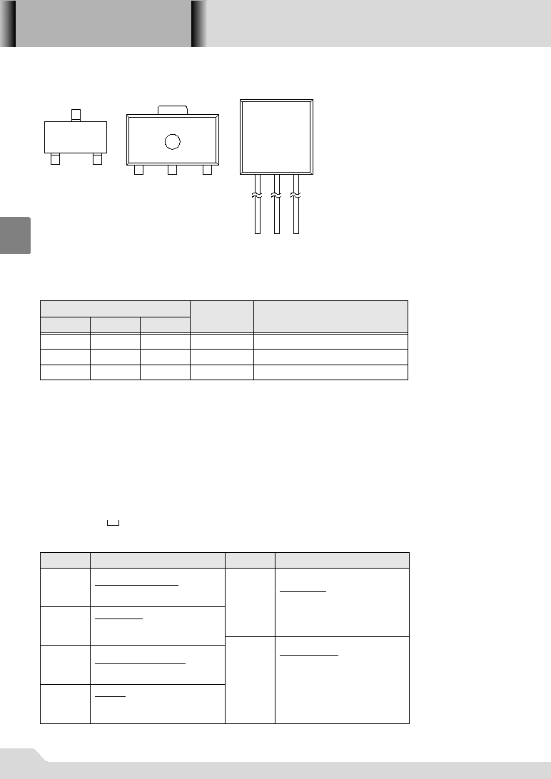
Product Classification
GOrdering Information
PIN NUMBER
SOT-23
TO-92
PIN NAME
FUNCTION
2
3
Power Supply Input
Ground
Output
3
2
1
SOT-89
3
2
1
1
≠V
IN
V
SS
≠V
OUT
SOT-23
TOP VIEW
SOT-89
TOP VIEW
3
1
2
-V
IN
-V
OUT
-
OUT
-
IN
V
SS
V
SS
1
2
3
DESIGNATOR
a
e
f
b
c
d
DESCRIPTION
DESIGNATOR
DESCRIPTION
Polarity of Output Voltage
N=Negative
Output Voltage
30=3.0V
50=5.0V
Temperature Characteristics
0=
±100ppm/∞C(typical)
Accuracy
1=
±1.0%(Semi-custom products)
2=
±2.0%
Package Type
M=SOT-23
P=SOT-89
T=TO-92 (Standard)
Device Orientation
R=Embossed Tape
(Standard Feed)
L=Embossed Tape
(Reverse Feed)
H=Paper Tape (TO-92)
B=Bag (TO-92)
X C 6 2 K X X X X X X X
a
b
c
d
e
f
1
2
3
TO-92
TOP VIEW
V
SS
-V
IN
-V
OUT
03S_10XC62K 02.9.12 3:08 PM 360
XC62K
Series
362
3
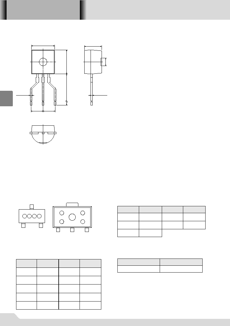
Marking
GSOT-23, SOT-89
q lntegral Number of Output Voltage
DESIGNATOR
2
3
4
VOLTAGE(V)
2.w
3.w
4.w
DESIGNATOR
5
6
VOLTAGE(V)
5.w
6.w
w Decimal number of Output Voltage
DESIGNATOR
A
B
C
D
E
F
H
K
L
M
q.0
q.1
q.2
q.3
q.4
q.5
q.6
q.7
q.8
q.9
VOLTAGE(V) DESIGNATOR VOLTAGE(V)
SOT-23
TOP VIEW
SOT-89
TOP VIEW
1 2 3 4
1
2
3
4
GTO-92
3.7±0.3
10.0min
1.6±0.1
0.4±0.05
4.65
0.45±0.1
2.5
+0.4
-0.1
2.5
+0.4
-0.1
+0.35
-0.45
4.8
+0.4
-0.5
e Polarity of Output Voltage
DESIGNATOR
POLARITY
5
Negative
r Assembly Lot Number
Based on internal standards.
03S_10XC62K 02.9.12 3:08 PM 362
XC62K
Series
363
3
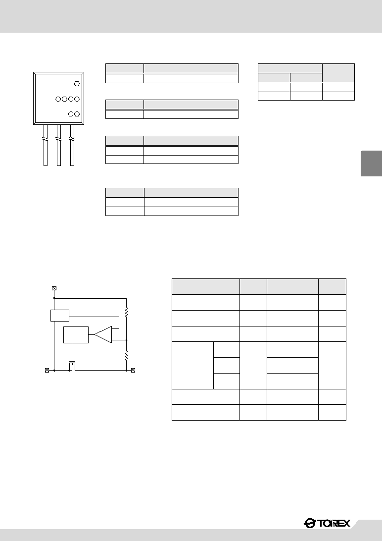
Absolute Maximum Ratings
Block Diagram
GTO-92
PARAMETER
Input Voltage
Output Voltage
SOT-23
Continuous
Total Power
Dissipation
TO-92
Operating Ambient
Temperature
Storage Temperature
RATINGS
≠12
≠V
DD
≠0.3 ~ V
IN
+0.3
150
300
SOT-89
500
≠30 ~ +80
≠40 ~ +125
UNITS
V
V
mW
∞C
∞C
SYMBOL
V
IN
V
OUT
Output Current
200
mA
I
OUT
P
d
T
opr
T
stg
Ta=25
∞C
Please ensure that I
OUT
is less than Pd
˜ (V
OUT
- V
IN
)
Note:
Current
Limit
Vref
V
SSGND
-V
IN
-V
OUT
+
-
2 3 4 5
6 7
1
TO-92T Type
(TOP VIEW)
62K
q Represents the Polarity of Output Voltage
DESIGNATOR
OUTPUT CONFIGURATION
N
--
we Represents the Detect Voltage
w
3
3.3
5
5.0
e
DESIGNATOR
VOLTAGEV
3
0
r Represents the temperature Characteristics
DESIGNATOR TEMPERATURE CHARACTERISTICS
0
TPY±100ppm
DESIGNATOR
DETECT VOLTAGE ACCURACY
1
within ±1semi-custom
2
within ±2
t Represents the Detect Voltage Accuracy
y Represents a least significant digit of the
produced year
DESIGNATOR
PRODUCED YEAR
0
2000
1
2001
u Denotes the production lot number
0 to 9, A to Z repeated(G.I.J.O.Q.W excepted)
03S_10XC62K 02.9.12 3:08 PM 363