
PFM Controlled, StepUp DC/DC Converters (Duty Ratio 58%)
Series
475
4
General Description
Features
Applications
Typical Application Circuit
Typical Performance
Characteristic
NDuty 58%
NCMOS Low Power Consumption
NOperating Voltage
: 0.9V~10.0V
NOutput Voltage Range
: 2.0V~7.0V
NOutput Voltage Accuracy: ±2.5%
The XC6381 series is a group of PFM controlled step-up DC/DC
converters.
The XC6381 series employs CMOS process and laser trimming
technologies so as to attain low power and high accuracy.
Max. oscillator frequency is trimmed to 155kHz (accuracy: ±15%).
Every built-in switching transistor type enables a step-up circuit to be
configured using only three external components ; a coil, a diode, and a
capacitor. External transistor versions are available to accommodate
high output current applications.
Both built-in and external transistor types include 5-pin and 3-pin
packages, which are provided with either a CE (chip enable) function that
reduces power consumption during shut-down mode, or a V
DD
pin
function (separated power and voltage detect pins).
SOT-23, SOT-25, and SOT-89-5 super mini-mold packages.
Operating (start-up) voltage range
: 0.9V~10V
Output voltage range : 2.0V~7.0V in 0.1V increments
Highly accurate
: Set-up voltage ±2.5%
Maximum oscillator frequency
: 155kHz (±15%)
Duty Ratio
: 58% (±5%)
Both built-in switching transistor and external types are
available
Five-lead packaged units offer either Chip Enable or
independent V
OUT
pin option.
Small package
: SOT-23, 25 mini-mold (3-pin, 5-pin)
SOT-89, 89-5 mini-power mold
(3-pin, 5-pin)
GCellular phones, pagers
GPalmtops
GCameras, video recorders
GPortable equipment
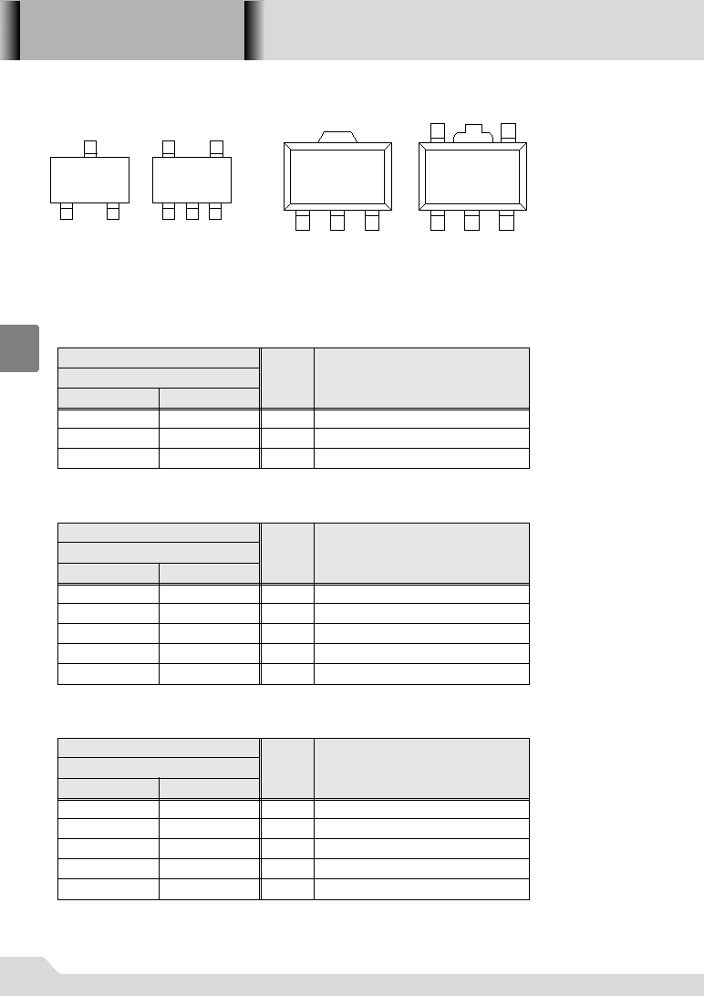
SOT-23
(TOP VIEW)
V
OUT
SD
2
1
3
GND
C
L
Tantalum
L
V
IN
C
IN
XC6381A301
L=100H,C=47FTantalum
100
80
60
40
20
0
0
20
40
60
80
100
Output Current:I
OUT
mA
Efficiency:EFFI
0.9V
1.2V
1.5V
1.8V
V
IN
=2.0V
04S_08XC6381 02.09.12 14:52 475
XC6381
Series
476
4
Pin Configuration
Pin Assignment
1
2
SOT-23
(TOP VIEW)
3
1
3
SOT-25
(TOP VIEW)
5
4
2
SOT-89
(TOP VIEW)
1
2
3
SOT-89-5
(TOP VIEW)
1
2
3
4
5
PIN NUMBER
XC6381A
XC6381A
1
3
2
PIN NAME
FUNCTION
V
SS
V
OUT
L
X
Ground
Output voltage monitor, IC internal power supply
Switch
SOT-23
SOT-89
1
2
3
PIN NUMBER
XC6381C
XC6381C
4
2
5
PIN NAME
FUNCTION
V
SS
V
OUT
L
X
Ground
Output voltage monitor, IC internal power supply
Switch
1
3
CE
Chip enable
NC
No connection
5
2
4
3
1
SOT-25
SOT-89-5
PIN NUMBER
XC6381E
XC6381E
PIN NAME
FUNCTION
V
SS
V
DD
L
X
Ground
IC internal power supply
Switch
V
OUT
Output voltage monitor
NC
No connection
4
2
5
1
3
5
2
4
3
1
SOT-25
SOT-89-5
04S_08XC6381 02.09.12 14:52 476

XC6381
Series
477
4
Product Classification
GSelection Guide
GOrdering Information
PART TYPE
PACKAGE
FEATURES
XC6381A
SOT-23,
SOT-89
SOT-25,
SOT-89-5
SOT-25,
SOT-89-5
∑
Accommodates a duty ratio of 58%.
XC6381C
∑
Stand-by (CE) function added version to the
XC6381A.
∑
Stand-by current: 0.5
µA max.
XC6381E
∑
Independent power supply and set-up voltage
sensing leads allow designing of PFM controllers.
ADDITIONAL
FUNCTION
Chip enable(CE)
≠
Separated
"V
DD
" and "V
OUT
" leads
DUTY
RATIO
58%
58%
58%
SWITCHING
RELATED
Built-in Transistor
"Lx" lead
Built-in Transistor
"Lx" lead
Built-in Transistor
"Lx" lead
P
R
L
A
C
E
1
3-pin. Built-in switching transistor
Stand-by capability. (5-pin) Built-in switching transistor
Separated V
DD
and V
OUT
. (5-pin) Built-in switching transistor
Maximum Oscillator Frequency 155kHz
Output Voltage
e.g.V
OUT
=3.5V
w=3, e=5
M
Package
q=A~B
SOT-23
q=C~F
SOT-25
Package
q=A~B
SOT-89
q=C~F
SOT-89-5
Embossed tape : Standard Feed
Embossed tape : Reverse Feed
XC6381 Series
PFM Controlled Duty 58%
XC6381qwerty
q
w
e
r
t
y
04S_08XC6381 02.09.12 14:52 477

XC6381
Series
478
4
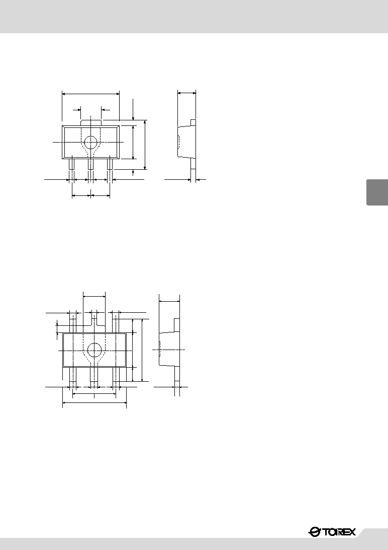
Packaging Information
GSOT-23
GSOT-25
1.1±0.1
00.1
0.15
0.95
1.9±0.2
2.9±0.2
0.2min
2.8±0.2
+0.1
-0.05
0.4
+0.1
-0.05
1.6
+0.2
-0.1
0.4
0.95
1.9±0.2
2.9±0.2
+0.1
-0.05
1.1±0.1
00.1
0.15
0.2min
+0.1
-0.05
2.8±0.2
1.6
+0.2
-0.1
04S_08XC6381 02.09.12 14:52 478
XC6381
Series
479
4
GSOT-89
GSOT-89-5
4.5±0.1
0.4
2.5±0.1
0.8
min
4.25max
0.42±0.06
0.4
1.5±0.1
0.47±0.06
1.5±0.1
0.42±0.06
1.5±0.1
1.6
+0.15
-0.2
+0.03
-0.02
0.42±0.06
0.42±0.06
0.42±0.06
1.5±0.1
0.8min
0.8min
4.5max
2.5±0.1
0.4
0.42±0.06
0.4
0.42±0.06
0.47±0.06
4.5±0.1
1.5±0.1 1.5±0.1
+0.03
-0.02
1.6
+0.15
-0.2
04S_08XC6381 02.09.12 14:52 479
XC6381
Series
480
4
SOT-89
(TOP VIEW)
q
w
e
r
2
1
4
3
SOT-89-5
(TOP VIEW)
Marking
SOT-23
(TOP VIEW)
q w e r
SOT-25
(TOP VIEW)
q w e r
w Represents the integer of the Output Voltage and Oscillator Frequency
1
155
OSCILLATOR FREQUENCYkHz
INTEGER OF THE
OUTPUT VOLTAGE
1
5
4
3
2
r Denotes the production lot number
0 to 9, A to Z repeated(G.I.J.O.Q.W excepted)
2
3
4
5
6
6
e Represents the decimal number of the Output Voltage and Oscillator Frequency
155
OSCILLATOR FREQUENCYkHz
OUTPUT VOLTAGE
0
9
8
7
6
1
5
4
3
2
0
9
8
7
6
1
5
4
3
2
q Represents the Product Classification
FUNCTION
Y
C
C
DESIGNATOR
-
CE
V
DD
/V
IN
PRODUCT NAME
XC6381A
XC6381C
XC6381E
Built-in Transistor
Built-in Transistor
Built-in Transistor
04S_08XC6381 02.09.12 14:52 480
XC6381
Series
481
4
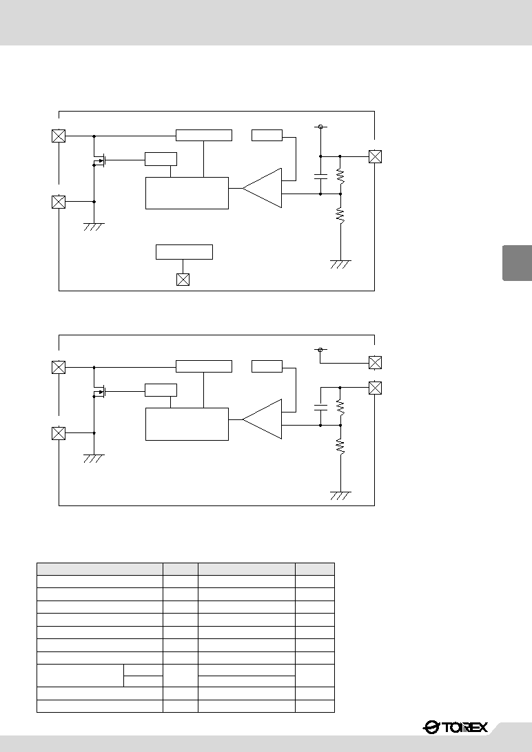
PFM Control OSC
155kHz
Buffer
VLx limiter
Vref
V
DD
Chip Enable
CE
+
-
XC6381A, XC6381C (V
OUT
pin can also be used for V
DD
pin.)
PFM Control OSC
155kHz
Buffer
VLx limiter
Vref
V
DD
+
-
XC6381E
Lx
V
SS
V
OUT
V
OUT
Lx
V
SS
V
DD
Built-in Tr types use the Lx pin, external Tr types use the EXT pin.
The CE pin is only used with the XC6381C.
Note:
The V
DD
pin is only used with the XC6381E.
Built-in Tr types use the Lx pin, external Tr types use the EXT pin.
Note:
Block Diagram
PARAMETER
SYMBOL
RATINGS
UNITS
V
OUT
Input Voltage
V
OUT
12
V
Lx pin Voltage
V
LX
12
V
Lx pin Current
I
LX
400
mA
EXT pin Voltage
V
EXT
V
SS
≠0.3~V
OUT
+0.3
V
EXT pin Current
I
EXT
±50
mA
CE Input Voltage
V
CE
12
V
V
DD
Input Voltage
V
DD
12
V
Continuous Total
SOT-23
SOT-89
150
Power Dissipation
P
D
500
mW
Operating Ambient Temperature
T
opr
≠30~+80
∞C
Storage Temperature
T
stg
≠40~+125
∞C
Ta=25
∞C
Absolute Maximum Ratings
04S_08XC6381 02.09.12 14:52 481
XC6381
Series
482
4
XC6381A501
Ta=25
∞C
V
OUT
=5.0V
PARAMETER
Output Voltage
Maximum Input Voltage
SYMBOL
V
OUT
L,SD,C
L
, etc. connected
V
IN
CONDITIONS
MIN
4.875
10
Oscillation Start-up Voltage
V
ST
I
OUT
=1mA
Oscillation Hold Voltage
V
HLD
I
OUT
=1mA
0.70
No-Load Input Current
I
IN
I
OUT
=0mA,(Note1)
Supply Current 1 (Note 2)
I
DD
1
V
IN
=V
OUT
0.95
Supply Current 2
I
DD
2
V
IN
=V
OUT
+0.5V
Lx Switch On-Resistance
R
SWON
Same as I
DD
1, V
LX
=0.4V
Lx Leakage Current
I
LXL
No external components, V
OUT
=V
LX
=10V
Duty Ratio
DTY
Same as I
DD
1
Measuring of Lx waveform
53
Maximum Oscillation Frequency
MAXF
OSC
Same as I
DD
1, 58% duty.
Same as I
DD
1, Fosc
MAXF
OSC
2
131.75
Lx Limit Voltage
VLxLMT
0.7
MAX
5.125
0.90
10.6
95.7
4.8
4.3
1.0
63
178.25
1.1
Efficiency
EFFI
L,SD,C
L
, etc. connected
TYP
5.000
0.80
5.3
47.8
2.4
2.8
58
155
85
UNITS
V
V
V
µA
µA
µA
µA
%
kHz
V
%
V
Measuring conditions: Unless otherwise specified, V
IN
=V
OUT
0.6, I
OUT
=50mA. See Typical application circuits, Fig.1.
1. The Schottky diode (SD) must be type MA735, with reverse current (I
R
) <1.0
µA at reverse voltage (V
R
)=10.0V.
2. "Supply current 1" is the supply current while the oscillator is continuously oscillating. In actual operation the oscillator periodically operates,
which results in less average power consumption. The current actually provided by an external V
IN
source is represented by "No-Load Input
Current (I
IN
)".
Note:
XC6381A301
Ta=25
∞C
V
OUT
=3.0V
PARAMETER
Output Voltage
Maximum Input Voltage
SYMBOL
V
OUT
L,SD,C
L
, etc. connected
V
IN
CONDITIONS
MIN
2.925
10
TYP
3.000
MAX
3.075
UNITS
V
Oscillation Start-up Voltage
V
ST
I
OUT
=1mA
0.80
0.90
V
Oscillation Hold Voltage
V
HLD
I
OUT
=1mA
0.70
V
No-Load Input Current
I
IN
I
OUT
=0mA,(Note1)
4.6
9.3
µA
Supply Current 1 (Note 2)
I
DD
1
V
IN
=V
OUT
0.95
29.3
58.7
µA
Supply Current 2
I
DD
2
V
IN
=V
OUT
+0.5V
2.1
4.2
µA
Lx Switch On-Resistance
R
SWON
Same as I
DD
1, V
LX
=0.4V
5.2
7.9
Lx Leakage Current
I
LXL
No external components, V
OUT
=V
LX
=10V
1.0
µA
Duty Ratio
DTY
Same as I
DD
1
Measuring of Lx waveform
53
58
63
%
Maximum Oscillation Frequency
MAXF
OSC
Same as I
DD
1, 58% duty.
131.75
155
178.25
kHz
Lx Limit Voltage
VLxLMT
Same as I
DD
1, Fosc
MAXF
OSC
2
0.7
1.1
V
Efficiency
EFFI
L,SD,C
L
, etc. connected
80
%
V
Measuring conditions: Unless otherwise specified, V
IN
=V
OUT
0.6, I
OUT
= 30mA. See Typical application circuits, Fig.1.
1. The Schottky diode (SD) must be type MA735, with reverse current (I
R
) <1.0
µA at reverse voltage (V
R
)=10.0V.
2. "Supply current 1" is the supply current while the oscillator is continuously oscillating. In actual operation the oscillator periodically operates,
which results in less average power consumption. The current actually provided by an external V
IN
source is represented by "No-Load Input
Current (I
IN
)".
Note:
Electrical Characteristics
04S_08XC6381 02.09.12 14:52 482
XC6381C501MR
Ta=25
∞C
V
OUT
=5.0V
PARAMETER
Output Voltage
Maximum Input Voltage
SYMBOL
L,SD,C
L
etc. connected
CONDITIONS
Oscillation Start-up Voltage
I
OUT
=1mA
Oscillation Hold Voltage
I
OUT
=1mA
No-Load Input Current
I
OUT
=0mA(Note1)
Supply Current 1 (Note 2)
V
IN
=V
OUT
0.95
Supply Current 2
V
IN
=V
OUT
+0.5V
Lx Switch-On Resistance
Same as I
DD
1. V
LX
=0.4V.
Lx Leakage Current
No external components. V
OUT
=V
LX
=10V.
Duty Ratio
Same as I
DD
1.
Measuring of L
X
waveform.
Maximum Oscillation Frequency
Same as I
DD
1. 58% duty.
Stand-by Current
Same as I
DD
1.
CE "High" Voltage
Same as I
DD
1.
Existence of Lx Oscillation.
Same as I
DD
1.
Disapperance of Lx Oscillation.
CE "Low" Voltage
CE "High" Current
Same as I
DD
1. V
CE
=V
OUT
0.95.
CE "Low" Current
Same as I
DD
1. V
CE
=0V.
Same as I
DD
1. F
OSC
>MAXF
OSC
2
Lx Limit Voltage
Efficiency
L,SD,C
L
etc. connected
Measuring conditions: Unless otherwise specified, connect CE to V
OUT
, V
IN
=V
OUT
0.6, I
OUT
=50mA. See Typical Application Circuits, Fig.2.
1. The Schottky diode (SD) must be type MA735, with reverse current (I
R
)<1.0
µA at reverse voltage (V
R
)=10.0V
2. "Supply Current 1" is the supply current while the oscillator is continuously oscillating. In actual operation the oscillator periodically operates
which results in less average power consumption. The current actually provided by an external V
IN
source is represented by "No-Load Input
Current (I
IN
)".
Note:
V
OUT
V
IN
MIN
4.875
10
V
ST
V
HLD
0.70
I
IN
I
DD
1
I
DD
2
R
SWON
I
LXL
DTY
53
MAXF
OSC
131.75
MAX
5.125
0.90
10.6
95.7
4.8
4.3
1.0
63
178.25
TYP
5.000
0.80
5.3
47.8
2.4
2.8
58
155
UNITS
V
V
V
µA
µA
µA
µA
%
kHz
I
STB
0.5
µA
V
CEH
0.75
V
V
CEL
0.20
V
I
CEH
0.25
µA
I
CEL
≠0.25
µA
VLxLMT
0.7
1.1
V
EFFI
85
%
V
XC6381C301MR
Ta=25
∞C
V
OUT
=3.0V
PARAMETER
Output Voltage
Maximum Input Voltage
SYMBOL
L,SD,C
L
etc. connected
CONDITIONS
Oscillation Start-up Voltage
I
OUT
=1mA
Oscillation Hold Voltage
I
OUT
=1mA
No-Load Input Current
I
OUT
=0mA, (Note1)
Supply Current 1 (Note 2)
V
IN
=V
OUT
0.95
Supply Current 2
V
IN
=V
OUT
+0.5V
Lx Switch-On Resistance
Same as I
DD
1. VL
X
=0.4V
Lx Leakage Current
No external components. V
OUT
=VL
X
=10V.
Duty Ratio
Same as I
DD
1.
Measuring of L
X
waveform.
Maximum Oscillation Frequency
Same as I
DD
1. 58% duty.
Stand-by Current
Same as I
DD
1.
CE "High" Voltage
Same as I
DD
1.
Existence of Lx Oscillation.
Same as I
DD
1.
Disappearance of Lx Oscillation.
CE "Low" Voltage
CE "High" Current
Same as I
DD
1. V
CE
=V
OUT
0.95.
CE "Low" Current
Same as I
DD
1. V
CE
=0V.
Lx Limit Voltage
Efficiency
L,SD,C
L
etc. connected
Measuring conditions: Unless otherwise specified, connect CE to V
OUT
, V
IN
=V
OUT
0.6, I
OUT
=30mA. See Typical Application Circuits, Fig.2.
1. The Schottky diode (SD) must be type MA735, with reverse current (I
R
)<1.0
µA at reverse voltage (V
R
)=10.0V
2. "Supply Current 1" is the supply current while the oscillator is continuously oscillating. In actual operation the oscillator periodically operates
which results in less average power consumption. The current actually provided by an external V
IN
source is represented by "No-Load Input
Current (I
IN
)".
Note:
V
OUT
V
IN
MIN
2.925
10
V
ST
V
HLD
0.70
I
IN
I
DD
1
I
DD
2
R
SWON
I
LXL
DTY
53
MAXF
OSC
131.75
UNITS
V
V
V
µA
µA
µA
µA
%
kHz
I
STB
0.5
µA
V
CEH
0.75
V
V
CEL
0.20
V
I
CEH
0.25
µA
I
CEL
≠0.25
µA
VLxLMT
0.7
1.1
V
EFFI
80
%
V
MAX
3.075
0.90
9.3
58.7
4.2
7.9
1.0
63
178.25
TYP
3.000
0.80
4.6
29.3
2.1
5.2
58
155
0.5
XC6381
Series
483
4
04S_08XC6381 02.09.12 14:52 483
XC6381
Series
484
4
Efficiency
XC6381E501MR
Ta=25
∞C
V
OUT
=5.0V
PARAMETER
Output Voltage
Maximum Input Voltage
SYMBOL
L,SD,C
L
etc. connected
CONDITIONS
Oscillation Start-up Voltage
I
OUT
=1mA
Oscillation Hold Voltage
I
OUT
=1mA
No-Load Input Current
I
OUT
=0mA,(Note1)
Supply Current 1 (Note 2)
V
IN
=V
OUT
0.95
Supply Current 2
V
IN
=V
OUT
+0.5V
Lx Switch-On Resistance
Same as I
DD
1. VL
X
=0.4V.
Lx Leakage Current
No external components. V
OUT
=VL
X
=10V.
Duty Ratio
Same as I
DD
1.
Measuring of L
X
waveform.
Maximum Oscillation Frequency
Same as I
DD
1. 58% duty.
Same as I
DD
1. F
OSC
>MAXF
OSC
2
Lx Limit Voltage
L,SD,C
L
etc. connected
Measuring conditions: Unless otherwise specified, connect V
DD
to V
OUT
, V
IN
=V
OUT
0.6, I
OUT
=50mA. See Typical Application Circuits, Fig.3.
1. The Schottky diode (SD) must be type MA735, with reverse current (I
R
)<1.0
µA at reverse voltage (V
R
)=10.0V.
2. "Supply Current 1" is the supply current while the oscillator is continuously oscillating. In actual operation the oscillator periodically operates
which results in less average power consumption. The current actually provided by an external V
IN
source is represented by "No-Load Input
Current (I
IN
)".
*
When the V
DD
and V
OUT
pins are independently used, the voltage range at the V
DD
pin should be 2.2V to 10V.
The IC operates from V
DD
=0.8V. However, output voltage and oscillator frequency are properly stabilized when V
DD
=2.2V or higher.
Note:
V
OUT
V
IN
MIN
4.875
10
V
ST
V
HLD
0.70
I
IN
I
DD
1
I
DD
2
R
SWON
I
LXL
DTY
53
MAXF
OSC
131.75
VLxLMT
0.7
MAX
5.125
0.90
10.6
95.7
48
4.3
1.0
63
178.25
1.1
EFFI
TYP
5.000
0.80
5.3
47.8
2.4
2.8
58
155
85
UNITS
V
V
V
µA
µA
µA
µA
%
kHz
V
%
V
Efficiency
XC6381E301MR
Ta=25
∞C
V
OUT
=3.0V
PARAMETER
Output Voltage
Maximum Input Voltage
SYMBOL
L,SD,C
L
etc. connected
CONDITIONS
Oscillation Start-up Voltage
I
OUT
=1mA.
Oscillation Hold Voltage
I
OUT
=1mA.
No-Load Input Current
I
OUT
=0mA(Note1)
Supply Current 1 (Note 2)
V
IN
=V
OUT
0.95
Supply Current 2
V
IN
=V
OUT
+0.5V
Lx Switch-On Resistance
Same as I
DD
1. VL
X
=0.4V
Lx Leakage Current
No external components. V
OUT
=VL
X
=10V
Duty Ratio
Same as I
DD
1
Measuring of L
X
waveform.
Maximum Oscillation Frequency
Same as I
DD
1. 58% duty.
Same as I
DD
1. F
OSC
>MAXF
OSC
2
Lx Limit Voltage
Efficiency
L,SD,C
L
etc. connected
Measuring conditions: Unless otherwise specified, connect V
DD
to V
OUT
, V
IN
=V
OUT
0.6, I
OUT
=30mA. See Typical Application Circuits, Fig.3.
1. The Schottky diode (SD) must be type MA735, with reverse current (I
R
)<1.0
µA at reverse voltage (V
R
)=10.0V.
2. "Supply Current 1" is the supply current while the oscillator is continuously oscillating. In actual operation the oscillator periodically operates
which results in less average power consumption. The current actually provided by an external V
IN
source is represented by "No-Load Input
Current (I
IN
)".
*
When the V
DD
and V
OUT
pins are independently used, the voltage range at the V
DD
pin should be 2.2V to 10V.
The IC operates from V
DD
=0.8V. However, output voltage and oscillator frequency are properly stabilized when V
DD
=2.2V or higher.
Note:
V
OUT
V
IN
MIN
2.925
10
V
ST
V
HLD
0.70
I
IN
I
DD
1
I
DD
2
R
SWON
I
LXL
DTY
53
MAXF
OSC
131.75
VLxLMT
0.7
MAX
3.075
0.90
9.3
58.7
4.2
7.9
1.0
63
178.25
1.1
EFFI
TYP
3.000
0.80
4.6
29.3
2.1
5.2
58
155
80
UNITS
V
V
V
µA
µA
µA
µA
%
kHz
V
%
V
04S_08XC6381 02.09.12 14:52 484
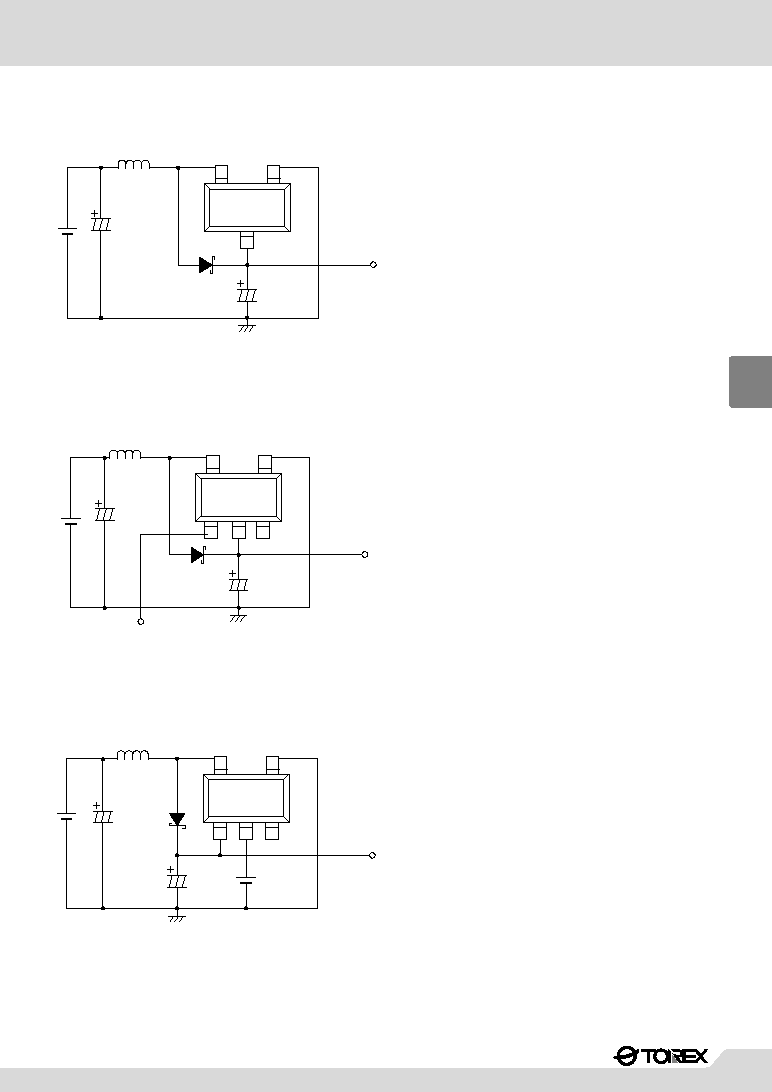
SOT-25
(TOP VIEW)
GND
V
OUT
SD
5
4
1
2
3
C
L
Tantalum
L
V
IN
V
DD
C
IN
L
: 100
µH (SUMIDA, CR-54)
SD : MA2Q735 (Schottky diode; MATSUSHITA)
C
L
: 16V 47
µF (Tantalum capacitor, NICHICON, MCE)
C
IN
: 16V 220
µF (Aluminium Electrolytic Capacitor)
Fig.3 XC6381E Application
SOT-23
(TOP VIEW)
V
OUT
SD
2
1
3
GND
C
L
Tantalum
L
V
IN
C
IN
L
: 100
µH (SUMIDA, CR-54)
SD : MA2Q735 (Schottky diode; MATSUSHITA)
C
L
: 16V 47
µF (Tantalum capacitor, NICHICON, MCE)
C
IN
: 16V 220
µF (Aluminium Electrolytic Capacitor)
Fig.1 XC6381A Application
Typical Application Circuits
XC6381
Series
485
4
L
: 100
µH (SUMIDA, CR-54)
SD : MA2Q735 (Schottky diode; MATSUSHITA)
C
L
: 16V 47
µF (Tantalum capacitor, NICHICON, MCE)
C
IN
: 16V 220
µF (Aluminium Electrolytic Capacitor)
Fig.2 XC6381C Application
SOT-25
(TOP VIEW)
V
OUT
5
4
2
1
3
CE
SD
GND
C
L
Tantalum
L
V
IN
C
IN
04S_08XC6381 02.09.12 14:52 485
XC6381
Series
486
4
Typical Performance Characteristics
XC6381A301
L=100H,C=47FTantalum
100
80
60
40
20
0
0
20
40
60
80
100
Output Current:I
OUT
mA
Efficiency:EFFI
0.9V
1.2V
1.5V
1.8V
V
IN
=2.0V
(2) EFFICIENCY vs. OUTPUT CURRENT
XC6381A301
Output Current:I
OUT
mA
Output Voltage:V
OUT
V
3.5
3.0
2.5
2.0
1.5
0.5
1.0
0.0
0
20
40
60
80
100
V
IN
=0.9V
1.2V
1.5V
1.8V
2.0V
L=100H,C=47FTantalum
(1) OUTPUT VOLTAGE vs. OUTPUT CURRENT
XC6381A301
L=100H,C=47FTantalum
100
80
60
40
20
0
Ripple Voltage:VrmVp-p
0
20
40
60
80
100
Output Current:I
OUT
mA
1.5V
1.2V
V
IN
=1.8V
(3) RIPPLE VOLTAGE vs. OUTPUT CURRENT
04S_08XC6381 02.09.12 14:52 486