TLN233
2002-01-17
1
TOSHIBA Infrared LED GaAAs Infrared Emitter
TLN233
Infrared LED for Space-Optical-Transmission
∑ High radiant intensity: 80 mW/sr (typ.) at I
F
= 50 mA
∑ Half-angle value: 1/2 = ±13∞ (typ.)
∑ A light source for remote control
∑ Wireless AV-signal transmission purpose
∑ High speed data transmission purpose
Maximum Ratings
(Ta
=
=
=
=
25∞C)
Characteristics Symbol
Rating
Unit
Forward current
I
F
100 mA
Pulse forward current
I
FP
1000
(Note 1)
mA
Power dissipation
P
D
200
mW
Reverse voltage
V
R
4
V
Operating temperature range
T
opr
-25~85 ∞C
Storage temperature range
T
stg
-30~100 ∞C
Soldering temperature (5 s), (Note 2)
T
sol
260
∞C
Note 1: f
= 100 kHz, duty = 1%
Note 2: Soldering must be performed under the stopper.
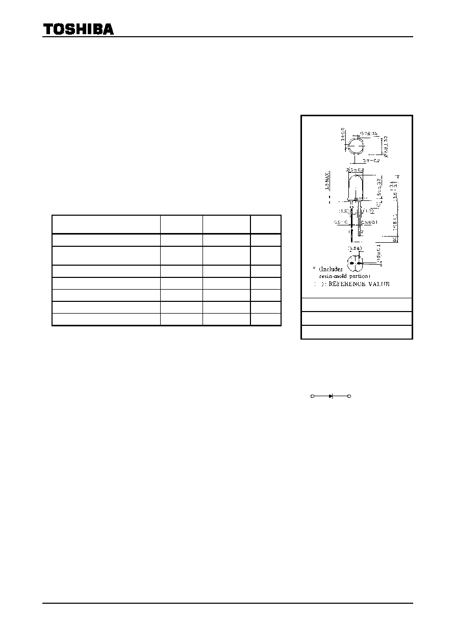
Unit: mm
JEDEC
JEITA
TOSHIBA 4-5V3
Pin Connection
1
2
1. Anode
2. Cathode

TLN233
2002-01-17
2
Optical and Electrical Characteristics
(Ta
=
=
=
=
25∞C)
Characteristics Symbol
Test
Condition
Min
Typ.
Max
Unit
Forward voltage
V
F
I
F
= 100 mA
æ 1.6 2.0 V
Reverse current
I
R
V
R
= 4 V
æ
æ 60 mA
Radiant intensity
I
E
I
F
= 50 mA
46
80
æ mW/sr
Radiant power
P
O
I
F
= 50 mA
æ 30 æ mW
Cut-off frequency
f
c
I
F
= 50 mA + 5 mA
P-P
(Note
3)
æ 15 æ MHz
Peak emission wavelength
l
P
I
F
= 50 mA
æ 870 æ nm
Half-angle value
q
2
1
I
F
= 50 mA
æ
±13
æ ∞
Note 3: Frequency when modulation light power decreases by 3dB from 1 MHz.
Handling Precautions
∑ Soldering must be performed under the stopper.
∑ When forming the leads, bend each lead under the 5 mm of package body. Soldering must be performed after the
leads have been formed.
∑ The radiant intensity decrease over time due to current flowing in the infrared LED. When designing circuits,
the device must take into account the change in radiant intensity over time. The change in radiant intensity is
equal to the reciprocal of the change in LED infrared optical output.
P (0)
o
P (t)
o
I (0)
E
I (t)
E
=

TLN233
2002-01-17
5
∑ TOSHIBA is continually working to improve the quality and reliability of its products. Nevertheless, semiconductor
devices in general can malfunction or fail due to their inherent electrical sensitivity and vulnerability to physical
stress. It is the responsibility of the buyer, when utilizing TOSHIBA products, to comply with the standards of
safety in making a safe design for the entire system, and to avoid situations in which a malfunction or failure of
such TOSHIBA products could cause loss of human life, bodily injury or damage to property.
In developing your designs, please ensure that TOSHIBA products are used within specified operating ranges as
set forth in the most recent TOSHIBA products specifications. Also, please keep in mind the precautions and
conditions set forth in the "Handling Guide for Semiconductor Devices," or "TOSHIBA Semiconductor Reliability
Handbook" etc..
∑ The TOSHIBA products listed in this document are intended for usage in general electronics applications
(computer, personal equipment, office equipment, measuring equipment, industrial robotics, domestic appliances,
etc.). These TOSHIBA products are neither intended nor warranted for usage in equipment that requires
extraordinarily high quality and/or reliability or a malfunction or failure of which may cause loss of human life or
bodily injury ("Unintended Usage"). Unintended Usage include atomic energy control instruments, airplane or
spaceship instruments, transportation instruments, traffic signal instruments, combustion control instruments,
medical instruments, all types of safety devices, etc.. Unintended Usage of TOSHIBA products listed in this
document shall be made at the customer's own risk.
∑ Gallium arsenide (GaAs) is a substance used in the products described in this document. GaAs dust and fumes
are toxic. Do not break, cut or pulverize the product, or use chemicals to dissolve them. When disposing of the
products, follow the appropriate regulations. Do not dispose of the products with other industrial waste or with
domestic garbage.
∑ The information contained herein is presented only as a guide for the applications of our products. No
responsibility is assumed by TOSHIBA CORPORATION for any infringements of intellectual property or other
rights of the third parties which may result from its use. No license is granted by implication or otherwise under
any intellectual property or other rights of TOSHIBA CORPORATION or others.
∑ The information contained herein is subject to change without notice.
000707EAC
RESTRICTIONS ON PRODUCT USE

