ICs for use with Crystal Oscillators
Series
1023
14
The XC2151 series are a group of high frequency, CMOS low power
crystal oscillators with oscillator & divider circuitry, oscillator capacitors
and amplifier feedback resistors built-in.
An oscillator circuit can be created from just an external crystal.
Output frequency can be selected from four frequencies :
Fundamental f0/1, Divided f0/2, f0/4, f0/8.
The output buffer is 3-State and has a fanout of 10 - TTL.
General Description
High Precision
: Built-in oscillator capacitors
16pF TYP (or selectable from 10 ~ 20pF)
: On-chip amplifier feedback resistor
5M
TYP (or selectable from 1.6k ~
8.4k
)
Oscillator Frequency : 4MHz ~ 70MHz
Divider Ratio
: Selectable from f0/1, f0/2, f0/4, f0/8
Output
: 3-State, 10 - TTL fanout
Operating Voltage Range
: 4.0V ~ 6.0V
Small Quiescent Current
Stand-By Function
Low Cost
: Oscillator circuit can be created from just
an external crystal
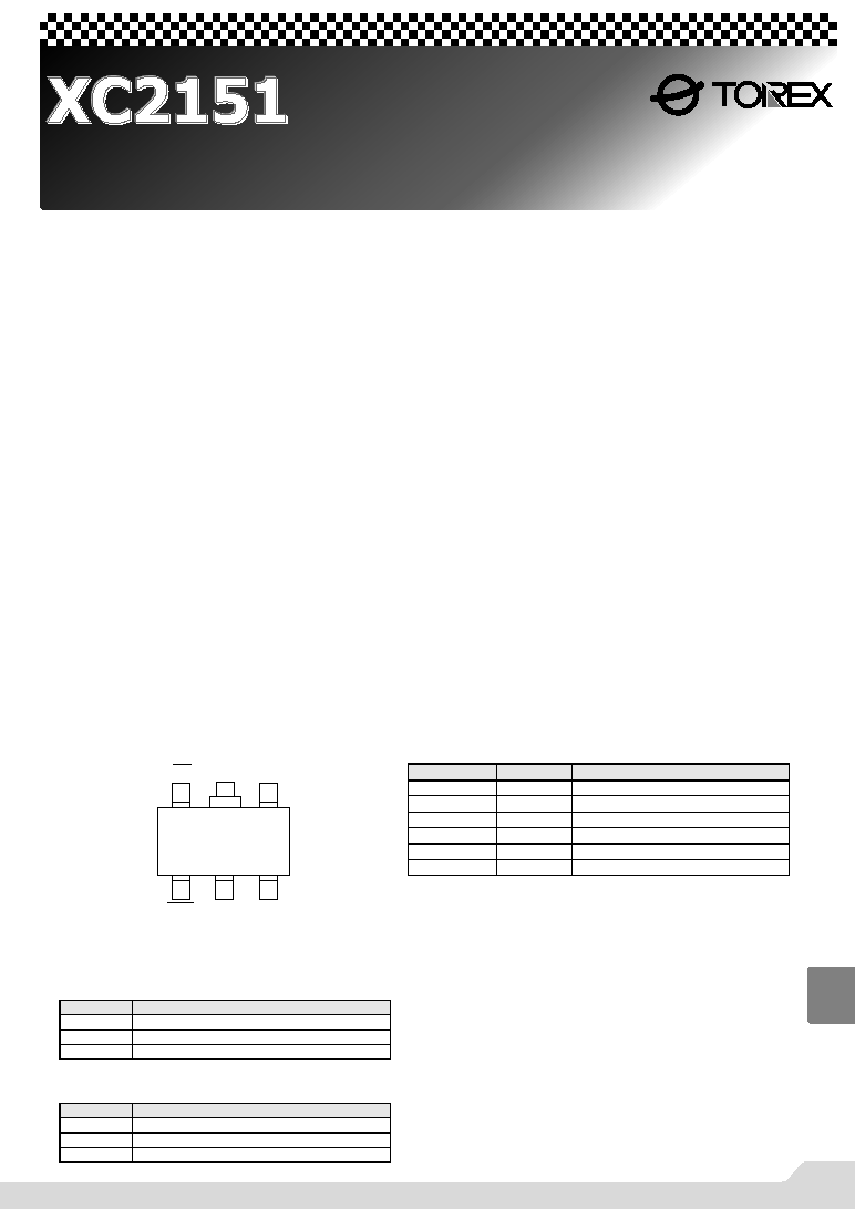
Ultra Small Package : SOT-26 (150mW) mini mold
GCrystal Oscillator Modules
GCommunication Equipment
GMicrocomputers
GClock Units in Motor Control
GSystem Clocks on Boards
GTimers
GPalmtops
Features
Applications
NCMOS
: Low Supply Current
NOscillator Frequency : 4MHz ~ 70MHz
NBuilt-In Oscillator Capacitors
NDivider Ratio
: fo/1, fo/2, fo/4, fo/8
N3-State Output
NSupply Voltage
: 5.0V
NMini Mold SOT-26 Package
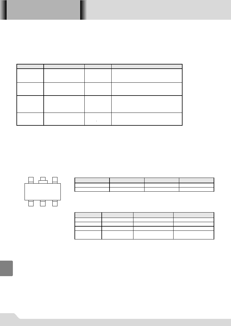
1
XT
XT
INH
SOT-26
(TOP VIEW)
Q
O
V
DD
V
SS
PIN NUMBER
PIN NAME
FUNCTION
1
/INH
Control *
2
XT
Oscillator Connection (Input)
3
V
SS
GND
4
Q
0
Output
5
V
DD
Power Supply
6
/XT
Oscillator Connection (Output)
* Control pin has pull-up resistor built-in.
XC2151x51
/INH
"H"
"L"
open
XC2151x55
/INH
"H"
"L"
open
"H" = High Level
"L" = Low Level
Output
High Impedance (oscillator stopped)
Q0
Output
Output
High Impedance (oscillator stopped)
Q0
Output
Pin Configuration
INH, Q
0
Pin Function
Pin Assignment
14S_03XC2151 02.09.12 16:35 1023
1024
14
Marking
SOT-26
(TOP VIEW)
q
w
e
r
q Represents the Divider Ratio
MARK
RATIO
RATIO
A
f0/1
f0/4
B
f0/2
MARK
C
D
f0/8
w Represents Stand-by Mode, Duty Level & Output Capability
MARK
STAND-BY MODE
DUTY LEVEL
OUTPUT CAPABILITY
5
CE
CMOS (V
DD
/2), TTL
10TTL
6
CE
CMOS (V
DD
/2) 10TTL
7
CE
TTL
10TTL
XC2151T=TTL ,
10TTL
XC2151C=CMOS
e Represents Fundamental / Overtone and Rf, Cg, Cd
r Represents the Assembly Lot No.
(based on internal standards)
8
OE
XC2151
Series
b c d e f g h
DESIGNATOR
DESCRIPTION
DESIGNATOR
DESCRIPTION
Supply Voltage :
Stand-by Mode and Divider Ratio :
a
5 = 5.0V
e
1=f0/1 (CE), 2=f0/2 (CE), 4=f0/4 (CE),
8=f0/8 (CE), 5=f0/1 (OE)
Product Series :
Fundamental / Overtone Rf, Cg, Cd :
b
1 = Large output capability,
f
(please refer to electrical characteristics tables)
fundamental & overtone
Duty Level :
Package :
c
A = CMOS (V
DD
/2) & TTL
g
M = SOT-26
C = CMOS (V
DD
/2)
T = TTL
Output Capability :
Device Orientation :
d
5 = 10TTL
h
R= Embossed Tape (Standerd Feed)
L= Embossed Tape (Reverse Feed)
Product Classification
GOrdering Information
14S_03XC2151 02.09.12 16:35 1024

1025
14
XC2151
Series
V
DD
Q
O
Q
O
V
SS
1/2
1/2
1/2
R
UP
XT
XT
INH
Rf
C
g
C
d
C
d
V
DD
V
SS
R
UP
XT
XT
INH
C
g
1) XC2151A Series
2) XC2151T/C Series
Block Diagram
PARAMETER
SYMBOL
CONDITIONS
UNITS
Supply Voltage
V
DD
V
SS
- 0.3 ~ V
SS
+ 7.0
V
Input Voltage
V
IN
V
SS
- 0.3 ~ V
DD
+ 0.3
V
Power Dissipation
Pd
150
mW
Operating Ambient Temp.
Topr
-30 ~ +75
O
C
Storage Temp.
Tstg
-55 ~ +125
O
C
Absolute Maximum Ratings
14S_03XC2151 02.09.12 16:35 1025
Electrical Characteristics
XC2151
Series
1026
14
XC2151T51A / 55A (overtone)
V
DD
=5.0V, Fosc=20MHz, No Load, Ta = 25
�C
Operating Supply Voltage
V
DD
4.0
6.0
V
Input Voltage 'High'
V
IH
2.4
V
Input Voltage 'Low'
V
IL
0.4
V
Output Current 'High'
I
OH
V
OH
= 4.6V
- 10
mA
Output Current 'Low'
I
OL
V
OL
= 0.4V
16
mA
Supply Current 1
I
DD1
/ INH = OPEN, Q
0
= OPEN
18
25
mA
Supply Current 2 (51A)
I
DD2
/ INH = "L"
2
5
�A
Supply Current 2 (55A)
I
DD2
/ INH = "L"
16
23
mA
Input Pull-Up Resistance
R
UP
/ INH = 4.5V
50
200
k
Internal Oscillator Capacitance
Cg,Cd
see note below
18
20
22
pF
Internal Oscillator Feedback Resistance
Rf
5.0
5.5
6.1
k
Output Disable Leakage Current
I
OZ
/ INH = "L"
10
�A
note : the values for Cg,Cd are the designed values.
XC2151T51D / 55D (overtone)
V
DD
=5.0V, Fosc=70MHz, No Load, Ta = 25
�C
Operating Supply Voltage
V
DD
4.0
6.0
V
Input Voltage 'High'
V
IH
2.4
V
Input Voltage 'Low'
V
IL
0.4
V
Output Current 'High'
I
OH
V
OH
= 4.6V
- 10
mA
Output Current 'Low'
I
OL
V
OL
= 0.4V
16
mA
Supply Current 1
I
DD1
/ INH = OPEN, Q
0
= OPEN
25
35
mA
Supply Current 2 (51D)
I
DD2
/ INH = "L"
2
5
�A
Supply Current 2 (55D)
I
DD2
/ INH = "L"
23
32
mA
Input Pull-Up Resistance
R
UP
/ INH = 4.5V
50
200
k
Internal Oscillator Capacitance
Cg,Cd
see note below
9
10
11
pF
Internal Oscillator Feedback Resistance
Rf
2.7
3.0
3.3
k
Output Disable Leakage Current
I
OZ
/ INH = "L"
10
�A
note : the values for Cg,Cd are the designed values.
XC2151T (overtone)
PART No. DUTY LEVEL
OUTPUT
DIVIDER RATIO
Rf (k
)
Cg/Cd (pF)
XC2151T51A TTL
10TTL
f0 / 1
5.5
20
XC2151T51B TTL
10TTL
f0 / 1
4.0
20
XC2151T51C TTL
10TTL
f0 / 1
3.0
13
XC2151T51D TTL
10TTL
f0 / 1
3.0
10
PARAMETER
PARAMETER
SYMBOL
SYMBOL
CONDITIONS
UNITS
MIN
TYP
MAX
MAX
RECOMMENDED
FREQUENCY RANGE
20MHz to 33MHz
30MHz to 45MHz
UNITS
MIN
TYP
CONDITIONS
43MHz to 57MHz
55MHz to 70MHz
14S_03XC2151 02.09.12 16:35 1026
XC2151C51F / 55F (overtone)
V
DD
=5.0V, Fosc=20MHz, No Load, Ta = 25
�C
Operating Supply Voltage
V
DD
4.0
6.0
V
Input Voltage 'High'
V
IH
2.4
V
Input Voltage 'Low'
V
IL
0.4
V
Output Current 'High'
I
OH
V
OH
= 4.6V
- 10
mA
Output Current 'Low'
I
OL
V
OL
= 0.4V
16
mA
Supply Current 1
I
DD1
/ INH = OPEN, Q
0
= OPEN
18
25
mA
Supply Current 2 (51F)
I
DD2
/ INH = "L"
2
5
�A
Supply Current 2 (55F)
I
DD2
/ INH = "L"
16
23
mA
Input Pull-Up Resistance
R
UP
/ INH = 4.5V
50
200
k
Internal Oscillator Capacitance
Cg,Cd
see note below
18
20
22
pF
Internal Oscillator Feedback Resistance
Rf
5.0
5.5
6.1
k
Output Disable Leakage Current
I
OZ
/ INH = "L"
10
�A
note : the values for Cg,Cd are the designed values.
XC2151C51L / 55L (overtone)
V
DD
=5.0V, Fosc=70MHz, No Load, Ta = 25
�C
Operating Supply Voltage
V
DD
4.0
6.0
V
Input Voltage 'High'
V
IH
2.4
V
Input Voltage 'Low'
V
IL
0.4
V
Output Current 'High'
I
OH
V
OH
= 4.6V
- 10
mA
Output Current 'Low'
I
OL
V
OL
= 0.4V
16
mA
Supply Current 1
I
DD1
/ INH = OPEN, Q
0
= OPEN
25
35
mA
Supply Current 2 (51L)
I
DD2
/ INH = "L"
2
5
�A
Supply Current 2 (55L)
I
DD2
/ INH = "L"
23
32
mA
Input Pull-Up Resistance
R
UP
/ INH = 4.5V
50
200
k
Internal Oscillator Capacitance
Cg,Cd
see note below
9
10
11
pF
Internal Oscillator Feedback Resistance
Rf
2.7
3.0
3.3
k
Output Disable Leakage Current
I
OZ
/ INH = "L"
10
�A
note : the values for Cg,Cd are the designed values.
XC2151C (overtone)
PART No. DUTY LEVEL
OUTPUT
DIVIDER RATIO
Rf (k
)
Cg/Cd (pF)
XC2151C51F CMOS (V
DD
/2)
10TTL
f0 / 1
5.5
20
XC2151C51H CMOS (V
DD
/2)
10TTL
f0 / 1
4.0
20
XC2151C51K CMOS (V
DD
/2)
10TTL
f0 / 1
3.0
13
XC2151C51L CMOS (V
DD
/2)
10TTL
f0 / 1
3.0
10
PARAMETER
SYMBOL
RECOMMENDED
20MHz to 33MHz
CONDITIONS
MIN
TYP
MAX
TYP
MAX
UNITS
UNITS
PARAMETER
SYMBOL
CONDITIONS
MIN
30MHz to 45MHz
43MHz to 57MHz
55MHz to 70MHz
XC2151
Series
1027
14
14S_03XC2151 02.09.12 16:35 1027