
1
XC6108 ETR0205_004.doc
CMOS
Highly Accurate
: +2%
Ultra Low Power Consumption
: 0.8
µA(TYP.)
(V
IN
= 2.0V)
Separated Sense Pin
Built-In Delay Circuit, Delay Pin Available
GENERAL DESCRIPTION
The XC6108 series is highly precise, low power
consumption voltage detector, manufactured using CMOS
and laser trimming technologies.
Since the sense pin is separated from power supply, it allows
the IC to monitor added power supply.
Using the IC with the sense pin separated from power supply
enables output to maintain the state of detection even when
voltage of the monitored power supply drops to 0V.
Moreover, with the built-in delay circuit, connecting the delay
capacitance pin to the capacitor enables the IC to provide an
arbitrary release delay time.
Both CMOS and N-channel open drain output configurations
are available.
APPLICATIONS
Microprocessor reset circuitry
Charge voltage monitors
Memory battery back-up switch circuits
Power failure detection circuits
FEATURES
Highly Accurate
:+2%
(Setting Detect Voltage1.5V)
:+30mV
(Setting Detect Voltage1.5V)
Ultra Low Power Consumption
:
0.8
µA (TYP.) (V
IN
= 2.0V)
Detect Voltage Range : 0.8V ~ 5.0V in 100mV increments
Operating Voltage Range : 1.0V ~ 6.0V
Detect Voltage Temperature Characteristics
:
±100ppm/
(TYP.)
Output Configuration
: CMOS or N-channel open drain
Operating Temperature Range
: -40
~ +85
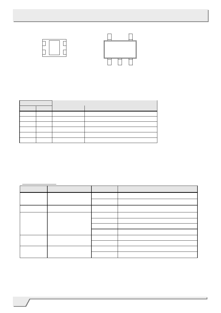
Ultra Small Package :
USP-4
SOT-25
TYPICAL APPLICATION CIRCUIT
VIN
VOUT
VSEN
Cd
VSS
R
100k
No resistor needed for
CMOS output product
Cd
VIN
Added
Power
Supply
TYPICAL PERFORMANCE
CHARACTERISTICS
Output Voltage vs. Sense Voltage
XC6108C25AGR
-1.0
0.0
1.0
2.0
3.0
4.0
5.0
6.0
7.0
0
1
2
3
4
5
6
Sense Voltage: VSEN (V)
O
u
tp
ut V
o
l
t
a
g
e
: V
O
U
T
(
V
)
Ta=25
4.0V
1.0V
VIN=6.0V
2
XC6108
Series
PIN NUMBER
USP- 4
SOT-25
PIN NAME
FUNCTION
1 1
V
OUT
Output (Detect "L")
2
5
Cd
Delay Capacitance (*1)
2 -
NC
No
Connection
3 4
V
SEN
Sense
4 3
V
IN
Input
5 2
V
SS
Ground
(*2)
DESIGNATOR
DESCRIPTION
SYMBOL
DESCRIPTION
C
: CMOS output
Output
Configuration
N
: N-ch open drain output
Detect Voltage
08 ~ 50
: e.g. 181.8V
A
: Built-in delay pin, hysteresis 5% (TYP.)
B
: Built-in delay pin, hysteresis less than 1%
C
: No built-in delay pin, hysteresis 5% (TYP.)
Output Delay & Hysteresis
(Options)
D
: No built-in delay pin, hysteresis less than 1%
G :
USP-4
Package
M :
SOT-25
R
: Embossed tape, standard feed
Device
Orientation
L
: Embossed tape, reverse feed
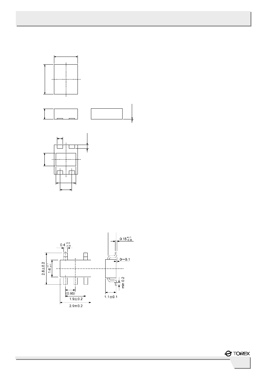
PIN CONFIGURATION
PIN ASSIGNMENT
PRODUCT CLASSIFICATION
XC6108
NOTE:
*1: With the V
SS
pin of the USP-4 package, a tab on the backside is used as the pin No.5.
*2: In the case of selecting no built-in delay pin type, the Cd pin will be used as the N.C.
VSS
VOUT
Cd
VIN
VSEN
1
2
4
3
5
1
2
3
4
5
Cd
VOUT
VIN
VSEN
VSS
USP-4
(BOTTOM VIEW)
SOT-25
(TOP VIEW)
* In the XC6108xxxA/B series, the dissipation pad should
not be short-circuited with other pins.
* In the XC6108xxxC/D series, when the dissipation pad
is short-circuited with other pins, connect it to the NC
pin (pin No.2) before use.
Ordering Information
3
XC6108
Series
PACKAGING INFORMATION
USP-4
SOT-25
0.
2
±
0.
1
MA
X
0
.
6
1. 0±0. 1
( 0. 6)
0.
7
±
0.
1
0. 3±0. 05
0.
00
7
+0
.
0
0
5
-0
.
0
0
4
1.
6
±
0.
08
1. 2±0. 08
* Soldering fillet surface is not formed
because the sides of the pins are plated.
4
XC6108
Series
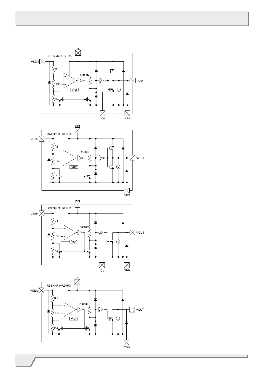
BLOCK DIAGRAMS
XC6108CxxA/B
XC6108CxxC/D
XC6108NxxA/B
XC6108NxxC/D
5
XC6108
Series
PARAMETER
SYMBOL
RATINGS
UNITS
Input Voltage
V
IN
V
SS
0.3 ~ 7.0
V
Output Current
I
OUT
10
mA
XC6108C (*1)
V
SS
0.3 ~ V
IN
0.3
Output Voltage
XC6108N (*2)
V
OUT
V
SS
0.3 ~ 7.0
V
Sense Pin Voltage
V
SEN
V
SS
0.3 ~ 7.0
V
Delay Pin Voltage
V
CD
V
SS
0.3 ~ V
IN
0.3
V
Delay Pin Current
I
CD
5.0 mA
USP-4 120
Power Dissipation
SOT-25
Pd
250
mW
Operating Temperature Range
Ta
40 ~85
Storage Temperature Range
Tstg
55 ~125
PARAMETER
SYMBOL
RATINGS
UNITS
Input Voltage
V
IN
V
SS
0.3 ~ 7.0
V
Output Current
I
OUT
10
mA
XC6108C (*1)
V
SS
0.3 ~ V
IN
0.3
Output Voltage
XC6108N (*2)
V
OUT
V
SS
0.3 ~ 7.0
V
Sense Pin Voltage
V
SEN
V
SS
0.3 ~ 7.0
V
USP-4 120
Power Dissipation
SOT-25
Pd
250
mW
Operating Temperature Range
Ta
40 ~85
Storage Temperature Range
Tstg
55 ~125
ABSOLUTE MAXIMUM RATINGS
XC6108xxxA/B
Ta = 25
O
C
XC6108xxxC/D
NOTE:
*1: CMOS output
*2: N-ch open drain output
Ta = 25
O
C
6
XC6108
Series
PARAMETER
SYMBOL
CONDITIONS
MIN.
TYP.
MAX.
UNITS
CIRCUITS
Operating Voltage
V
IN
V
DF(T)
= 0.8 ~ 5.0V (*1)
1.0
-
6.0
V
-
Detect Voltage
V
DF
V
IN
= 1.0 ~ 6.0V
E-1
V
1
Hysteresis Range1
V
HYS1
V
IN
= 1.0 ~ 6.0V
E-2
V
1
Detect Voltage
Line Regulation
V
DF
V
IN
V
DF
V
IN
= 1.0 ~ 6.0V
-
±0.1
-
%/V
1
V
IN
= 1.0V
- 0.6 1.5
Supply Current 1 (*2)
I
SS1
V
SEN
=
V
DF
x 0.9
V
IN
= 6.0V
-
0.7
1.6
µA
2
V
IN
= 1.0V
- 0.8 1.7
Supply Current 2
(*2)
I
SS2
V
SEN
=
V
DF
x 1.1
V
IN
= 6.0V
-
0.9
1.8
µA
2
V
IN
= 1.0V
0.08
0.20
-
V
SEN
=0V
V
DS
= 0.5V (N-ch)
V
IN
= 6.0V
1.20
2.00
-
mA 3
V
IN
= 1.0V
-
-0.30
-0.08
Output Current
(*3)
I
OUT
V
SEN
= 6.0V
V
DS
= 0.5V (P-ch)
V
IN
= 6.0V
-
-2.00
-0.70
mA 4
Temperature
Characteristics
V
DF
TaV
DF
-40
Ta 85
- ±100
-
ppm/
1
Sense Resistance
(*4)
R
SEN
VSEN = 5.0V, V
IN
= 0V
E-4
M
5
Delay Resistance
(*5)
Rdelay
V
SEN
= 6.0V, V
IN
= 5.0V,
Cd = 0V
1.6 2.0 2.4 M
6
Delay pin
Sink Current
I
CD
V
DS
= 0.5V, V
IN
= 1.0V
-
200
-
µA
6
V
SEN
= 6.0V, V
IN
= 1.0V
0.4
0.5
0.6
Delay Capacitance Pin
Threshold Voltage
V
TCD
V
SEN
= 6.0V, V
IN
= 6.0V
2.9
3.0
3.1
V
7
Unspecified Operating
Voltage (*6)
V
UNS
V
IN
= V
SEN
= 0V ~ 0.7V
-
0.3
0.4
V
8
Detect Delay Time (*7)
T
DF0
V
IN
= 6.0V, V
SEN
= 6.0V0.0V
Cd: Open
30
230
µs
9
Release Delay Time
(*8)
T
DR0
V
IN
= 6.0V, V
SEN
= 0.0V6.0V
Cd: Open
30
200
µs
9
NOTE:
*1: V
DF(T):
Setting detect voltage
*2: Current flows the sense resistor is not included.
*3: This numerical value is applied only to the XC6108C series (CMOS output).
*4: Calculated from the voltage value and the current value of the V
SEN
.
*5: Calculated from the voltage value of the V
IN
and the current value of the Cd.
*6: The maximum voltage of the V
OUT
in the range of the V
IN
0V to 0.7V when the V
IN
and the V
SEN
are short-circuited
This numerical value is applied only to the XC6108C series (CMOS output).
*7: Time which ranges from the state of V
SEN
=V
DF
to the V
OUT
reaching 0.6V when the V
SEN
falls without connecting to the Cd pin.
*8: Time which ranges from the state of V
IN
= V
DF
+V
HYS
to the V
OUT
reaching 5.4V when the V
SEN
rises without connecting to the Cd pin
.
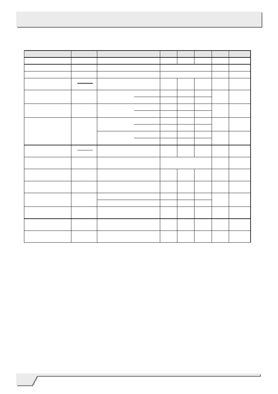
ELECTRICAL CHARACTERISTICS
XC6108xxxA
Ta=25

7
XC6108
Series
PARAMETER
SYMBOL
CONDITIONS
MIN.
TYP.
MAX.
UNITS
CIRCUITS
Operating Voltage
V
IN
V
DF(T)
= 0.8 ~ 5.0V (*1)
1.0
-
6.0
V
-
Detect Voltage
V
DF
V
IN
= 1.0 ~ 6.0V
E-1
V
1
Hysteresis Range1
V
HYS1
V
IN
= 1.0 ~ 6.0V
E-3
V
1
Detect Voltage
Line Regulation
V
DF
V
IN
V
DF
V
IN
= 1.0 ~ 6.0V
-
±0.1
-
%/V
1
V
IN
= 1.0V
- 0.6 1.5
Supply Current 1 (*2)
I
SS1
V
SEN
=
V
DF
x 0.9
V
IN
= 6.0V
-
0.7
1.6
µA
2
V
IN
= 1.0V
- 0.8 1.7
Supply Current 2
(*2)
I
SS2
V
SEN
=
V
DF
x 1.1
V
IN
= 6.0V
-
0.9
1.8
µA
2
V
IN
= 1.0V
0.08
0.20
-
V
SEN
=0V
V
DS
= 0.5V (N-ch)
V
IN
= 6.0V
1.20
2.00
-
mA 3
V
IN
= 1.0V
-
-0.30
-0.08
Output Current
(*3)
I
OUT
V
SEN
= 6.0V
V
DS
= 0.5V (P-ch)
V
IN
= 6.0V
-
-2.00
-0.70
mA 4
Temperature
Characteristics
V
DF
TaV
DF
-40
Ta 85
- ±100
-
ppm/
1
Sense Resistance
(*4)
R
SEN
V
SEN
= 5.0V, V
IN
= 0V
E-4
M
5
Delay Resistance
(*5)
Rdelay
V
SEN
= 6.0V, V
IN
= 5.0V,
Cd = 0V
1.6 2.0 2.4 M
6
Delay pin
Sink Current
I
CD
V
DS
= 0.5V, V
IN
= 1.0V
-
200
-
µA
6
V
SEN
= 6.0V, V
IN
= 1.0V
0.4
0.5
0.6
Delay Capacitance Pin
Threshold Voltage
V
TCD
V
SEN
= 6.0V, V
IN
= 6.0V
2.9
3.0
3.1
V
7
Unspecified Operating
Voltage (*6)
V
UNS
V
IN
= V
SEN
= 0V ~ 0.7V
-
0.3
0.4
V
8
Detect Delay Time
(*7)
T
DF0
V
IN
= 6.0V, V
SEN
= 6.0V0.0V
Cd: Open
30
230
µs
9
Release Delay Time
(*8)
T
DR0
V
IN
= 6.0V, V
SEN
= 0.0V6.0V
Cd: Open
30
200
µs
9
ELECTRICAL CHARACTERISTICS (Continued)
XC6108xxxB
Ta=25
NOTE:
*1: V
DF(T):
Setting detect voltage
*2: Current flows the sense resistor is not included.
*3: This numerical value is applied only to the XC6108C series (CMOS output).
*4: Calculated from the voltage value and the current value of the V
SEN.
*5: Calculated from the voltage value of the V
IN
and the current value of the Cd.
*6: The maximum voltage of the V
OUT
in the range of the V
IN
0V to 0.7V when the V
IN
and the V
SEN
are short-circuited
This numerical value is applied only to the XC6108C series (CMOS output).
*7: Time which ranges from the state of V
SEN
=V
DF
to the V
OUT
reaching 0.6V when the V
SEN
falls without connecting to the Cd pin.
*8: Time which ranges from the state of V
IN
= V
DF
+V
HYS
to the V
OUT
reaching 5.4V when the V
SEN
rises without connecting to the Cd pin.
8
XC6108
Series
PARAMETER
SYMBOL
CONDITIONS
MIN.
TYP.
MAX.
UNITS
CIRCUITS
Operating Voltage
V
IN
V
DF(T)
= 0.8 ~ 5.0V (*1)
1.0
-
6.0
V
-
Detect Voltage
V
DF
V
IN
= 1.0 ~ 6.0V
E-1
V
1
Hysteresis Range1
V
HYS1
V
IN
= 1.0 ~ 6.0V
E-2
V
1
Detect Voltage
Line Regulation
V
DF
V
IN
V
DF
V
IN
= 1.0 ~ 6.0V
-
±0.1
-
%/V
1
V
IN
= 1.0V
- 0.6 1.5
Supply Current 1 (*2)
I
SS1
V
SEN
=
V
DF
x 0.9
V
IN
= 6.0V
-
0.7
1.6
µA
2
V
IN
= 1.0V
- 0.8 1.7
Supply Current 2
(*2)
I
SS2
V
SEN
=
V
DF
x 1.1
V
IN
= 6.0V
-
0.9
1.8
µA
2
V
IN
= 1.0V
0.08
0.20
-
V
SEN
=0V
V
DS
= 0.5V (N-ch)
V
IN
= 6.0V
1.20
2.00
-
mA 3
V
IN
= 1.0V
-
-0.30
-0.08
Output Current
(*3)
I
OUT
V
SEN
= 6.0V
V
DS
= 0.5V (P-ch)
V
IN
= 6.0V
-
-2.00
-0.70
mA 4
Temperature
Characteristics
V
DF
TaV
DF
-40
Ta 85
- ±100
-
ppm/
1
Sense Resistance
(*4)
R
SEN
V
SEN
= 5.0V, V
IN
= 0V
E-4
M
5
Unspecified Operating
Voltage (*5)
V
UNS
V
IN
= V
SEN
= 0V ~ 0.7V
-
0.3
0.4
V
7
Detect Delay Time (*6)
T
DF0
V
IN
= 6.0V, V
SEN
= 6.0V0.0V
30
230
µs
9
Release Delay Time
(*7)
T
DR0
V
IN
= 6.0V, V
SEN
= 0.0V6.0V
30
200
µs
9
ELECTRICAL CHARACTERISTICS (Continued)
XC6108xxxC
Ta=25
NOTE:
*1: V
DF(T):
Setting detect voltage
*2: Current flows the sense resistor is not included.
*3: This numerical value is applied only to the XC6108C series (CMOS output).
*4: Calculated from the voltage value and the current value of the V
SEN
.
*5: The maximum voltage of the V
OUT
in the range of the V
IN
0V to 0.7V when the V
IN
and the V
SEN
are short-circuited
This numerical value is applied only to the XC6108C series (CMOS output).
*6: Time which ranges from the state of V
SEN
=V
DF
to the V
OUT
reaching 0.6V when the V
SEN
falls.
*7: Time which ranges from the state of V
IN
= V
DF
+V
HYS
to the V
OUT
reaching 5.4V when the V
SEN
rises.
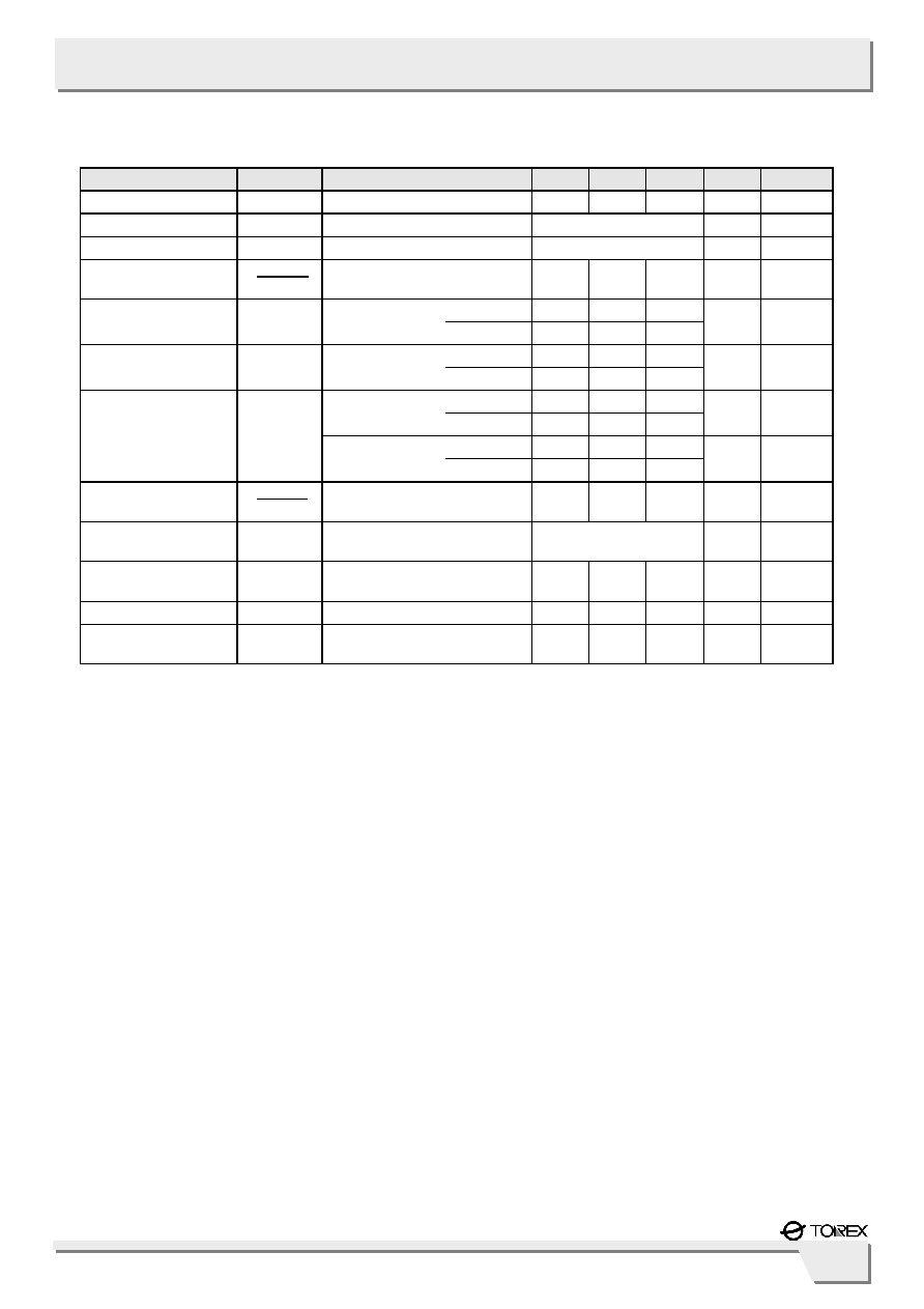
9
XC6108
Series
PARAMETER
SYMBOL
CONDITIONS
MIN.
TYP.
MAX.
UNITS
CIRCUITS
Operating Voltage
V
IN
V
DF(T)
= 0.8 ~ 5.0V (*1)
1.0
-
6.0
V
-
Detect Voltage
V
DF
V
IN
= 1.0 ~ 6.0V
E-1
V
1
Hysteresis Range1
V
HYS1
V
IN
= 1.0 ~ 6.0V
E-3
V
1
Detect Voltage
Line Regulation
V
DF
V
IN
V
DF
V
IN
= 1.0 ~ 6.0V
-
±0.1
-
%/V
1
V
IN
= 1.0V
- 0.6 1.5
Supply Current 1 (*2)
I
SS1
V
SEN
=
V
DF
x 0.9
V
IN
= 6.0V
-
0.7
1.6
µA
2
V
IN
= 1.0V
- 0.8 1.7
Supply Current 2
(*2)
I
SS2
V
SEN
=
V
DF
x 1.1
V
IN
= 6.0V
-
0.9
1.8
µA
2
V
IN
= 1.0V
0.08
0.20
-
V
SEN
=0V
V
DS
= 0.5V (N-ch)
V
IN
= 6.0V
1.20
2.00
-
mA 3
V
IN
= 1.0V
-
-0.30
-0.08
Output Current
(*3)
I
OUT
V
SEN
= 6.0V
V
DS
= 0.5V (P-ch)
V
IN
= 6.0V
-
-2.00
-0.70
mA 4
Temperature
Characteristics
V
DF
TaV
DF
-40
Ta 85
- ±100
-
ppm/
1
Sense Resistance
(*4)
R
SEN
V
SEN
= 5.0V, V
IN
= 0V
E-4
M
5
Unspecified Operating
Voltage (*5)
V
UNS
V
IN
= V
SEN
= 0V ~ 0.7V
-
0.3
0.4
V
7
Detect Delay Time (*6)
T
DF0
V
IN
= 6.0V, V
SEN
= 6.0V0.0V
30
230
µs
9
Release Delay Time
(*7)
T
DR0
V
IN
= 6.0V, V
SEN
= 0.0V6.0V
30
200
µs
9
ELECTRICAL CHARACTERISTICS (Continued)
XC6108xxxD
Ta=25
NOTE:
*1: V
DF(T):
Setting detect voltage
*2: Current flows the sense resistor is not included.
*3:
This numerical value is applied only to the XC6108C series (CMOS output).
*4: Calculated from the voltage value and the current value of the V
SEN
.
*5: The maximum voltage of the V
OUT
in the range of the V
IN
0V to 0.7V when the V
IN
and the V
SEN
are short-circuited
This numerical value is applied only to the XC6108C series (CMOS output).
*6: Time which ranges from the state of V
SEN
=V
DF
to the V
OUT
reaching 0.6V when the V
SEN
falls.
*7: Time which ranges from the state of V
IN
= V
DF
+V
HYS
to the V
OUT
reaching 5.4V when the V
SEN
rises.
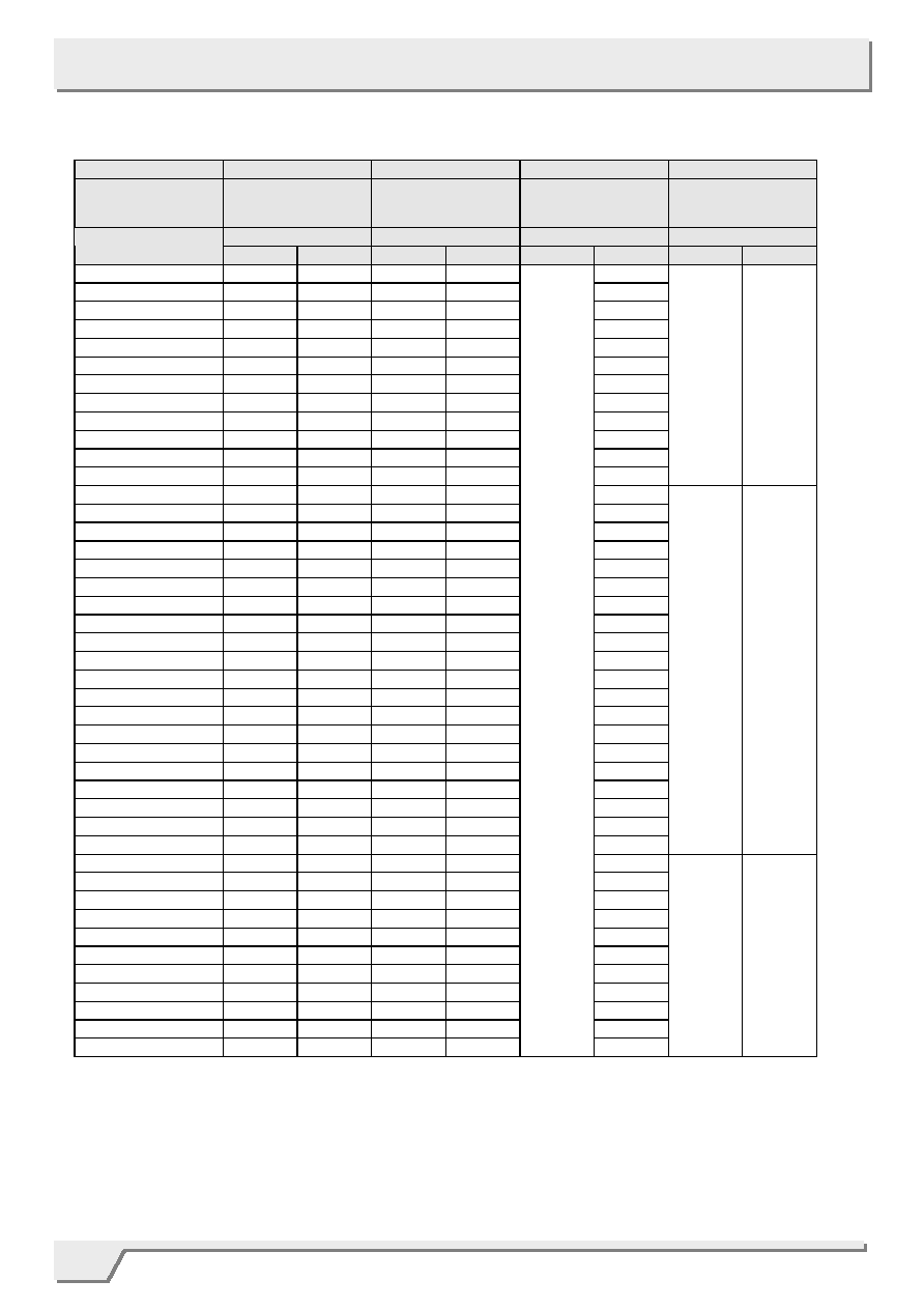
10
XC6108
Series
SYMBOL
E-1
E-2
E-3
E-4
SETTING OUTPUT
VOLTAGE
DETECT VOLTAGE
(*1) (V)
HYSTERESIS
RANGE
(V)
HYSTERESIS
RANGE
(V)
SENSE
RESISTANCE
(M)
V
DF
V
HYS
V
HYS
R
SEN
V
DF(T)
(V)
MIN.
MAX.
MIN.
MAX.
MIN.
MAX.
MIN.
TYP.
0.8 0.770
0.830
0.015 0.066
0.008
0.9 0.870
0.930
0.017 0.074
0.009
1.0 0.970
1.030
0.019 0.082
0.010
1.1
1.070 1.230 0.021 0.090
0.011
1.2 1.170
1.230
0.023 0.098
0.012
1.3 1.270
1.330
0.025 0.106
0.013
1.4
1.370 1.430 0.027 0.114
0.014
1.5 1.470
1.530
0.029 0.122
0.015
1.6 1.568
1.632
0.031 0.131
0.016
1.7 1.666
1.734
0.033 0.085
0.017
1.8 1.764
1.836
0.035 0.147
0.018
1.9 1.862
1.938
0.037 0.155
0.019
10 20
2.0 1.960
2.040
0.039 0.163
0.020
2.1 2.058
2.142
0.041 0.171
0.021
2.2 2.156
2.244
0.043 0.180
0.022
2.3 2.254
2.346
0.045 0.188
0.023
2.4 2.352
2.448
0.047 0.196
0.024
2.5 2.450
2.550
0.049 0.204
0.026
2.6 2.548
2.652
0.051 0.212
0.027
2.7 2.646
2.754
0.053 0.220
0.028
2.8 2.744
2.856
0.055 0.228
0.029
2.9 2.842
2.958
0.057 0.237
0.030
3.0 2.940
3.060
0.059 0.245
0.031
3.1 3.038
3.162
0.061 0.253
0.032
3.2 3.136
3.264
0.063 0.261
0.033
3.3 3.234
3.366
0.065 0.269
0.034
3.4 3.332
3.468
0.067 0.277
0.035
3.5 3.430
3.570
0.069 0.286
0.036
3.6 3.528
3.672
0.071 0.294
0.037
3.7 3.626
3.774
0.073 0.302
0.038
3.8 3.724
3.876
0.074 0.310
0.039
3.9 3.822
3.978
0.076 0.318
0.040
13 24
4.0 3.920
4.080
0.078 0.326
0.041
4.1 4.018
4.182
0.080 0.335
0.042
4.2 4.116
4.284
0.082 0.343
0.043
4.3 4.214
4.386
0.084 0.351
0.044
4.4 4.312
4.488
0.086 0.359
0.045
4.5 4.410
4.590
0.088 0.367
0.046
4.6 4.508
4.692
0.090 0.375
0.047
4.7 4.606
4.794
0.092 0.384
0.048
4.8 4.704
4.896
0.094 0.392
0.049
4.9 4.802
4.998
0.096 0.400
0.050
5.0
4.900 5.100 0.098 0.408
0
0.051
15 28
VOLTAGE CHART
NOTE:
*1: When V
DF(T)
1.4V, the detection accuracy is ±30mV.
When V
DF(T)
1.5V, the detection accuracy is ±2%.
11
XC6108
Series
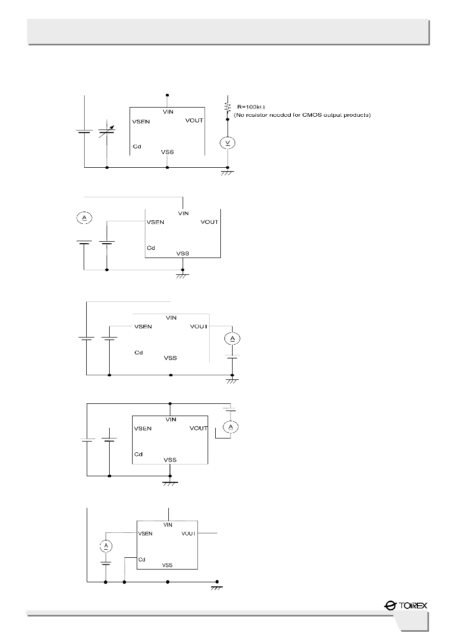
TEST CIRCUITS
Circuit 1
Circuit 2
Circuit 3
Circuit 4
Circuit 5

12
XC6108
Series
Circuit 9
TEST CIRCUITS (Continued)
Circuit 6
Circuit 7
Circuit 8
VIN
Cd
VSS
VOUT
Waveform Measurement Point
VSEN
(No resistor needed for
CMOS output products)
R=100k
* No delay capacitance pin available
in the XC6108xxxC/D series.

13
XC6108
Series
Delay Capacitance [Cd]
(F)
Release Delay Time [T
DR
]
(TYP.)
(ms)
Release Delay Time [T
DR
]
(MIN. ~ MAX.)
(ms)
0.010
13.8
11.0 ~ 16.6
0.022
30.4
24.3 ~ 36.4
0.047
64.9
51.9 ~ 77.8
0.100
138
110 ~ 166
0.220 304
243~
364
0.470
649
519 ~ 778
1.000
1380
1100 ~ 1660
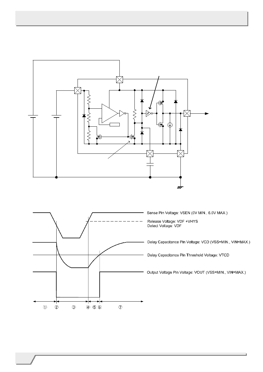
OPERATIONAL EXPLANATION
A typical circuit example is shown in Figure 1, and the timing chart of Figure 1 is shown in Figure 2 on the next page.
As an early state, the sense pin is applied sufficiently high voltage (6.0V MAX.) and the delay capacitance (Cd) is charged
to the power supply input voltage, (V
IN
: 1.0V MIN., 6.0V MAX.). While the sense pin voltage (V
SE
N
) starts dropping to
reach the detect voltage (V
DF
) (V
SEN
>V
DF
), the output voltage (V
OUT
) keeps the "High" level (=V
IN
).
* If a pull-up
resistor of the XC6108N series (N-ch open drain) is connected to added power supply different from the input
voltage pin, the "High" level will be a voltage value where the pull-up resistor is connected.
When the sense pin voltage keeps dropping and becomes equal to the detect voltage, an N-ch transistor for the delay
capacitance discharge is turned ON, and starts to discharge the delay capacitance. For the internal circuit, which uses
the delay capacitance pin as power input, the reference voltage operates as a comparator of V
IN
, and the output voltage
changes into the "Low" level (=V
SS
). The detect delay time [T
DF
] is defined as time which ranges from V
SEN
=V
DF
to the
V
OUT
of "Low" level (especially, when the Cd pin is not connected: T
DF0
).
While the sense pin voltage keeps below the detect voltage, the delay capacitance is discharged to the ground voltage
(=V
SS
) level. Then, the output voltage maintains the "Low" level while the sense pin voltage increases again to reach the
release voltage (V
SEN
< V
DF
+V
HYS
).
When the sense pin voltage continues to increase up to the release voltage level (V
DF
+V
HYS
), the N-ch transistor for the
delay capacitance discharge will be turned OFF, and the delay capacitance will start discharging via a delay resistor
(Rdelay). The internal circuit, which uses the delay capacitance pin as power input, will operate as a hysteresis
comparator (Rise Logic Threshold: V
TLH
=V
TCD
, Fall Logic Threshold: V
THL
=V
SS
) while the sense pin voltage keeps
higher than the detect voltage (V
SEN
> V
DF
).
While the delay capacitance pin voltage (V
CD
) rises to reach the delay capacitance pin threshold voltage (V
TCD
) with the
sense pin voltage equal to the release voltage or higher, the sense pin will be charged by the time constant of the RC
series circuit. Assuming the time to the release delay time (T
DR
), it can be given by the formula (1).
T
DR
=
Rdelay
◊
Cd
◊
In (1
V
TCD
/ V
IN
) ...(1)
* In = a natural logarithm
The release delay time can also be briefly calculated with the formula (2) because the delay resistance is 2.0M(TYP.) and
the delay capacitance pin voltage is V
IN /2
(TYP.)
T
DR
= 2.0e6
◊
Cd
◊
0.69...(2)
As an example, presuming that the delay capacitance is 0.68F, T
DR
is :
2.0e6
◊
0.68e
6
◊
0.69 = 938 (ms)
* Note that the release delay time may remarkably be short when the delay capacitance is not discharged to the ground
(=V
SS
) level because time described in is short.
When the delay capacitance pin voltage reaches to the delay capacitance pin threshold voltage (V
CD
=V
TCD
), output of an
internal circuit, which uses the delay capacitance pin as power input will be inverted. As a result, the output voltage
changes into the "High" (=V
IN
) level. T
DR0
is defined as time which ranges from V
SEN
=V
DF
+V
HYS
to the V
OUT
of "High"
level without connecting to the Cd.
While the sense voltage is higher than the detect voltage (V
SEN
> V
DF
), the delay capacitance pin is charged until the
delay capacitance pin voltage becomes the input voltage level. Therefore, the output voltage maintains the "High"(=V
IN
)
level.
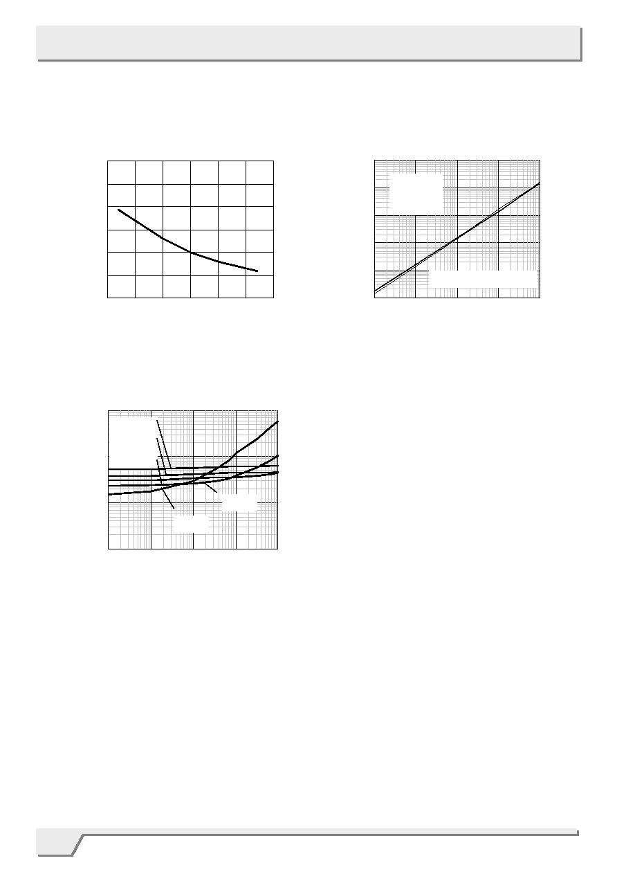
Release Delay Time Chart
14
XC6108
Series
OPERATIONAL EXPLANATION (Continued)
Figure 1: Typical application circuit example
Figure 2: The timing chart of Figure 1
+
-
VIN
VSEN
VOUT
Cd
VSS
Vref
Rdelay
R1
RSEN
=R1+R2+R3
R2
R3
External Delay
Capacitor [Cd]
N-ch transistor for the
delay capacitance
discharge
VSEN
VIN
The circuit which uses the delay
capacitance pin as power input.
* In the XC6108N series (N-ch open
drain output), a pull-up resistor for
pulling up output is required.
15
XC6108
Series
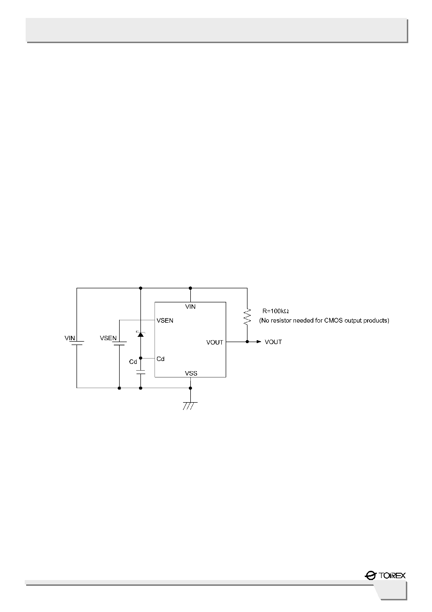
1. Use this IC within the stated maximum ratings. Operation beyond these limits may cause degrading or permanent
damage to the device.
2. The power supply input pin voltage drops by the resistance between power supply and the V
IN
pin, and by through
current at operation of the IC. At this time, the operation may be wrong if the power supply input pin voltage falls below
the minimum operating voltage range. In CMOS output, for output current, drops in the power supply input pin voltage
similarly occur. Moreover, in CMOS output, when the V
IN
pin and the sense pin are short-circuited and used,
oscillation of the circuit may occur if the drops in voltage, which caused by through current at operation of the IC, exceed
the hysteresis voltage. Note it especially when you use the IC with the V
IN
pin connected to a resistor.
3. When the setting voltage is less than 1.0V, be sure to separate the V
IN
pin and the sense pin, and to apply the voltage
over 1.0V to the V
IN
pin.
4. Note that a rapid and high fluctuation of the power supply input pin voltage may cause a wrong operation.
5. When there is a possibility of which the power supply input pin voltage falls rapidly (e.g.: 6.0V to 0V) at release
operation with the delay capacitance pin (Cd) connected to a capacitor, use a schottky barrier diode connected between
the V
IN
pin and the Cd pin as the Figure 3 shown below.
6. In N-ch open drain output, a pull-up resistor connected to the output voltage pin should be 100k-200k.
Figure 3: Circuit example with the delay capacitance pin (Cd) connected to a schottky barrier diode
NOTES ON USE
16
XC6108
Series
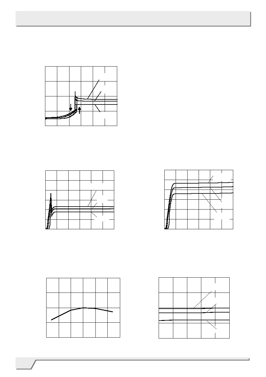
TYPICAL PERFORMANCE CHARACTERISTICS
(1) Supply Current vs. Sense Voltage
(2) Supply Current vs. Input Voltage
(3) Detect Voltage vs. Ambient Temperature
(4) Detect Voltage vs. Input Voltage
XC6108C25AGR
0.0
0.5
1.0
1.5
2.0
0
1
2
3
4
5
6
Sense Voltage: VSEN (V)
Su
p
p
l
y
C
u
r
r
e
n
t:
ISS
(
µ
A
)
25
-40
Ta=85
VIN=3.0V
XC6108C25AGR
2.45
2.50
2.55
-50
-25
0
25
50
75
100
Ambient Temperature: Ta ()
D
e
t
e
c
t
V
o
l
t
age:
V
D
F
(
V
)
VIN=4.0V
XC6108C25AGR
0.0
0.2
0.4
0.6
0.8
1.0
1.2
0
1
2
3
4
5
6
Input Voltage: VIN (V)
S
uppl
y
C
u
r
r
ent
:
I
S
S
(
µ
A
)
VSEN=2.25V
25
-40
Ta=85
XC6108C25AGR
0.0
0.2
0.4
0.6
0.8
1.0
1.2
0
1
2
3
4
5
6
Input Voltage: VIN (V)
S
uppl
y
C
u
r
r
ent
:
I
S
S
(
µ
A
)
VSEN=2.75V
25
-40
Ta=85
XC6108C25AGR
2.45
2.50
2.55
1.0
2.0
3.0
4.0
5.0
6.0
Input Voltage: VIN (V)
D
e
t
e
c
t
V
o
l
t
ag
e:
V
D
F
(
V
)
85
-40
Ta=25

17
XC6108
Series
TYPICAL PERFORMANCE CHARACTERISTICS (Continued)
(5) Hysteresis Voltage vs. Ambient Temperature
(6) CD Pin Sink Current vs. Input Voltage
(7) Output Voltage vs. Sense Voltage
(8) Output Voltage vs. Input Voltage
(9) Output Current vs. Input Voltage
XC6108C25AGR
0.05
0.10
0.15
0.20
-50
-25
0
25
50
75
100
Ambient Temperature: Ta ()
H
y
s
t
er
e
s
i
s
V
o
l
t
age
:
VH
YS
(
V
)
VIN=4.0V
XC6108C25AGR
-1.0
0.0
1.0
2.0
3.0
4.0
5.0
6.0
7.0
0
1
2
3
4
5
6
Sense Voltage: VSEN (V)
O
u
t
put
V
o
l
t
a
ge:
V
O
U
T
(
V
)
Ta=25
4.0V
1.0V
VIN=6.0V
XC6108C25AGR
0.0
0.5
1.0
1.5
2.0
2.5
3.0
0
1
2
3
4
5
6
Input Voltage: VIN (V)
C
d
P
I
N S
i
n
k
Cu
r
r
e
n
t
:
I
C
D
(
m
A
)
25
85
Ta=-40
VSEN=0V, VDS=0.5V
XC6108N25AGR
-1.0
0.0
1.0
2.0
3.0
4.0
0
0.5
1
1.5
2
2.5
3
Input Voltage: VIN (V)
O
u
tp
u
t
V
o
l
t
a
g
e
:
VO
U
T
(
V
)
25
-40
Ta=85
VSEN=VIN, Pull-up=VIN, R=100k
XC6108C25AGR
0.0
0.5
1.0
1.5
2.0
2.5
3.0
3.5
4.0
0
1
2
3
4
5
6
Input Voltage: VIN (V)
O
u
tp
u
t
C
u
r
r
e
n
t: IO
U
T
(
m
A
)
VDS(Nch)=0.5V
Ta=-40
25
85
XC6108C25AGR
-2.0
-1.5
-1.0
-0.5
0.0
0
1
2
3
4
5
6
Input Voltage: VIN (V)
O
u
t
put
C
u
r
r
en
t
:
I
O
U
T
(
m
A
)
VDS(Pch)=0.5V
-40
25
Ta=85
18
XC6108
Series
TYPICAL PERFORMANCE CHARACTERISTICS (Continued)
(10) Delay Resistance vs. Ambient Temperature
(11) Release Delay Time vs. Delay Capacitance
(12) Detect Delay Time vs. Delay Capacitance
XC6108C25AGR
1
1.5
2
2.5
3
3.5
4
-50
-25
0
25
50
75
100
Ambient Temperature: Ta ()
D
e
l
a
y R
e
si
st
a
n
ce
:
R
d
e
l
a
y
(
M
)
VSEN=6.0V, VCD=0.0V, VIN=5.0V
XC6108C25AGR
1
10
100
1000
0.0001
0.001
0.01
0.1
1
Delay Capacitance: Cd (µF)
D
e
te
c
t
D
e
l
a
y
T
i
m
e
: T
D
F
(µ
s)
Ta=25
VIN=6.0V
4.0V
3.0V
2.0V
1.0V
XC6108C25AGR
0.1
1
10
100
1000
10000
0.0001
0.001
0.01
0.1
1
Delay Capacitance: Cd (µF)
Re
l
e
a
s
e
D
e
l
a
y
T
i
m
e
:
T
D
R
(m
s
)
Ta=25
TDR=Cd◊2.0e6◊0.69
VIN=1.0V
3.0V
6.0V