2 Channel Voltage Detectors
Series
169
2
General Description
Features
Applications
V
IN
V
IN2
V
DET1
V
SS
V
IN1
V
DET2
R
R=100k
V
DET1
CMOS, V
DET2
N-ch Open drain
Typical Application Circuit
Typical Performance
Characteristic
SUPPLY CURRENT vs. INPUT VOLTAGE
GMemory battery back-up circuitry
GMicroprocessor reset circuits
GPower failure detection
GSystem power-on reset circuits
GSystem battery life monitors and re-charge voltage monitors
GDelay circuitry
NCMOS Low Power Consumption
N2 Voltage Detectors Built-in
NDetect Voltage Accuracy : � 2%
NDetect Voltage Range
: 1.5V ~ 5.0V
NSOT-25 Package
The XC612 series consist of 2 voltage detectors, in 1 mini-molded, SOT-
25 package.
The series provides accuracy and low power consumption through
CMOS processing and laser trimming and consists of a highly accurate
voltage reference source, 2 comparators, hysteresis and output driver
circuits.
The input (V
IN1
) for voltage detector 1 (V
D1
) dually functions as the power
supply pin for both detector 1 (V
D1
) and detector 2 (V
D2
).
Highly accurate
: Set-up voltage accuracy �2%
Low-power consumption
: Typ.2.0
�A (V
IN1
=V
IN2
=2.0V, quiescent state)
Detect voltage
: 1.5V ~ 5.0V programmable in
0.1V steps. Detector's voltages
can be set-up independently
Conditionaly,
XC612N : V
DET1
>V
DET2
XC612D, XC612E : V
DET1
V
DET2
,
V
DET1
<V
DET2
Operating Voltage Range : 1.
0V ~ 10.0V
Temperature characteristics : �100ppm/�C
Output configuration
: N-channel open drain
Small package
: SOT-25 (150mW) mini-mold
* CMOS Output is under development
0
1.0
2.0
3.0
4.0
5.0
6.0
0
2
4
6
8
10
25
Ta=80
-30
Supply Current: Iss (
�
A)
Input Voltage: V
IN1
(V)
(V
IN1
V
IN2
)
02S_05XC612 02.09.12 14:15 169

XC612
Series
170
2
Pin Configuration
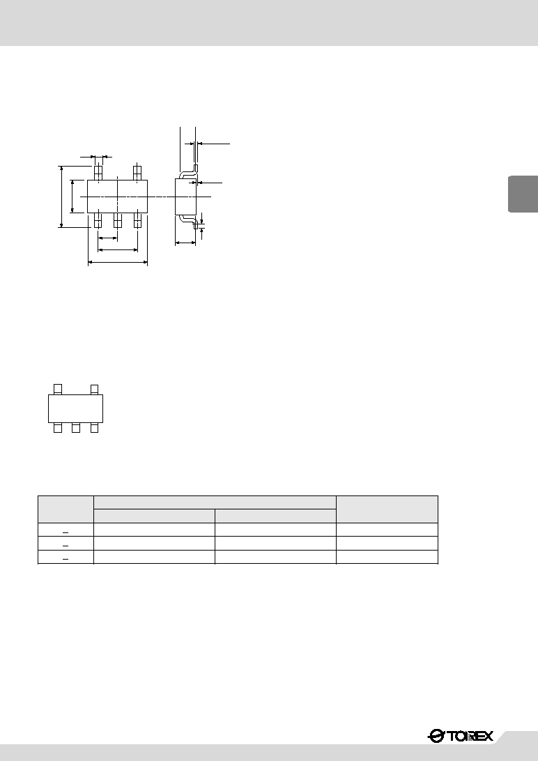
Pin Assignment
Product Classification
GSelection Guide
GOrdering Information
SOT-25
TOP VIEW
5
4
V
DET2
V
DET1
IN2
V
IN1
V
SS
1
3
2
PIN NUMBER
1
PIN NAME
FUNCTION
2
4
5
Detector 1 input,
Power Supply.
Voltage Detector 1 output
Voltage Detector 2 Input
Voltage Detector 2 Output
3
Ground
V
DET1
V
IN2
V
DET2
V
IN1
V
SS
Type
V
DET1
V
DET2
XC612N
N-ch Open drain
N-ch Open drain
XC612D
N-ch Open drain
CMOS
XC612E
CMOS
N-ch Open drain
a b c d e
XC612 x x x x x x x
e.g.33=3.3V
50=5.0V
DESIGNATOR
a
d
e
b
c
DESCRIPTION
DESIGNATOR
DESCRIPTION
Output Configuration:
N=N-Channel Open Drain
D=V
DET1
N-ch Open Drain, V
DET2
CMOS
E=V
DET1
CMOS, V
DET2
N-ch Open Drain
Detect Voltage (V
DET1
)
e.g.25=2.5V
38=3.8V
Detect Voltage (V
DET2
)
Package Type:
M=SOT-25
Device Orientation
R=Embossed Tape (Orientation of Device: Right)
L=Embossed Tape (Orientation of Device: Left)
02S_05XC612 02.09.12 14:15 170
XC612
Series
171
2
Marking
Packaging Information
GSOT-25
0.4
0.95
1.9�0.2
2.9�0.2
+0.1
-0.05
1.1�0.1
00.1
0.15
0.2min
+0.1
-0.05
2.8�0.2
1.6
+0.2
-0.1
SOT-25
(TOP VIEW)
DESIGNATOR
N
D
E
CONFIGURATION
V
DET1
N-ch Open drain
N-ch Open drain
CMOS
V
DET2
N-ch Open drain
CMOS
N-ch Open drain
PRODUCT NAME
XC612N****M*
XC612D****M*
XC612E****M*
q Represents the output configuration
we Represents the entry order.
r Denotes the production lot number
0 to 9, A to Z repeated. (G.I.J.O.Q.W excepted)
02S_05XC612 02.09.12 14:15 171