Low Voltage DetectorsV
DF
=0.9V1.5V
Series
131
2
The XC61C series are highly precise, low power consumption voltage
detectors, manufactured using CMOS and laser trimming technologies.
Detect voltage is extremely accurate with minimal temperature drift.
Both CMOS and N-channel open drain output configurations are
available.
General Description
Highly accurate
: ± 2%
Low power consumption : TYP 0.7
µA [ V
IN
=1.5V ]
Detect voltage range
: 0.9V ~ 1.5V in 0.1V increments
Operating voltage range : 0.7V ~ 6.0V
Detect voltage temperature characteristics
: TYP± 100ppm/∞C
Output configuration
: N-channel open drain or CMOS
Ultra small package
: SSOT-24 (150mW) super mini-mold
: SOT-23 (150mW) mini-mold
: SOT-89 (500mW) mini-power mold
: TO-92 ( 300mW )
Note : There are no products available with a set-up voltage
accuracy of ± 1%.
GMicroprocessor reset circuitry
GMemory battery back-up circuits
GPower-on reset circuits
GPower failure detection
GSystem battery life and charge voltage monitors
Features
Applications
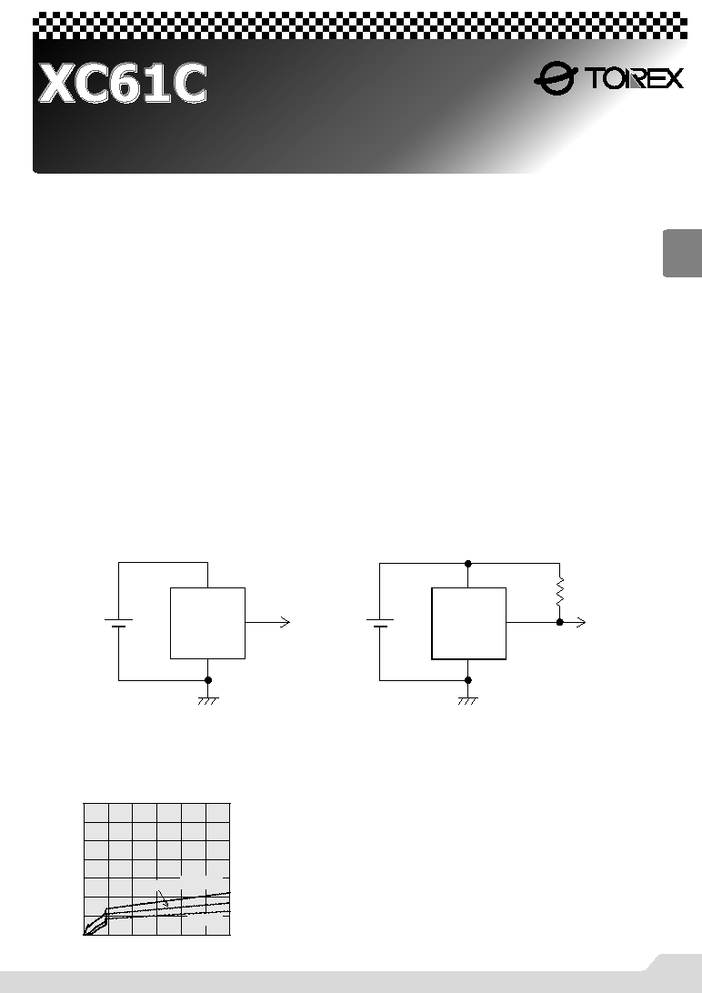
NCMOS
NHighly Accurate
: ± 2%
NLow Power Consumption : 0.7µA (V
IN
= 1.5V)
NUltra small SSOT-24 (SC-82) Package
0
0.5
1.0
1.5
2.0
2.5
3.0
3.5
0
1
2
3
4
5
6
Ta=85
-40
25
(.)
Input Voltage: V
IN
(V)
Supply Current: I
SS
(A)
CMOS Output
N-ch Open Drain Output
R
100k
V
IN
V
OUT
V
SS
V
IN
V
OUT
V
SS
V
IN
V
IN
Typical Application Circuits
Typical Performance Characteristic
SUPPLY CURRENT vs. INPUT VOLTAGE
02S_02XC61C 02.09.12 14:23 131

XC61C
Series
132
2
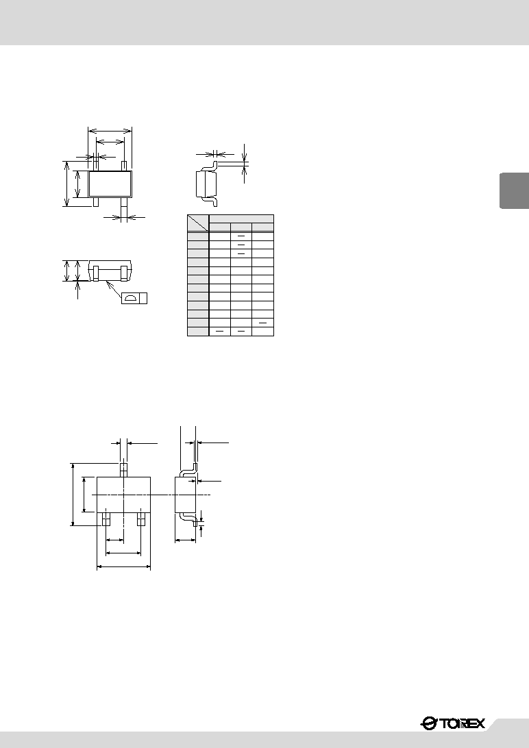
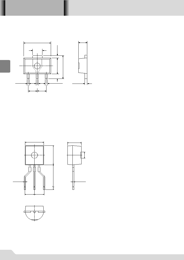
Pin Configuration
Pin Assignment
Product Classification
GOrdering Information
1
SOT-23
(TOP VIEW)
V
IN
V
SS
V
OUT
1
V
IN
NC
V
SS
V
OUT
SSOT-24(SC-82)
(TOP VIEW)
SOT-89
(TOP VIEW)
V
IN
1
V
SS
V
OUT
PIN
SSOT-24
SOT-23
SOT-89
NAME
2
3
2
V
IN
Supply Voltage Input
4
2
3
V
SS
Ground
1
1
1
V
OUT
Output
3
-
-
-
-
TO-92 (T)
2
3
1
TO-92 (L)
1
2
3
NC
No Connection
FUNCTION
PIN NUMBER
XC61C x x x x x x x
a b c d e f
Output Configuration :
Package Type:
C = CMOS
N = SSOT-24 (SC-82)
N = N-ch open drain
M = SOT-23
Detect Voltage :
P = SOT-89
09 = 0.9V
15 = 1.5V
Output Delay :
Device Orientation :
0 = No delay
R = Embossed Tape ( Right )
L = Embossed Tape ( Left )
Detect Accuracy :
2 =
within ± 2.0%
d
e
f
DESCRIPTION
DESIGNATOR
DESCRIPTION
DESIGNATOR
a
b
c
T = TO-92 (Standard)
L = TO-92 (Custom pin Configuration)
H = Paper Type ( TO-92)
B = Bag ( TO-92 )
1
2
3
TO-92 (T Type)
TOP VIEW
V
OUT
V
IN
V
SS
1
2
3
TO-92 (L Type)
TOP VIEW
V
IN
V
SS
V
OUT
02S_02XC61C 02.09.12 14:23 132

XC61C
Series
135
2
Marking
GSSOT-24, SOT-23, SOT-89
SOT-23
(TOP VIEW)
q w e r
SSOT-24(SC-82)
(TOP VIEW)
q
r
w
SOT-89
(TOP VIEW)
q
w
e
r
q Represents the integer of the Output Voltage and Detect Voltage
CMOS Output (XC61CC series)
N-Channel Open Drain Output (XC61CN series)
VOLTAGE (V)
CMOS
N-ch
CMOS
N-ch
w Represents the decimal number of the Detect Voltage
e Based on internal standards
( SSOT-24 excepted )
r Represents the assembly lot no.
Based on internal standards
DESIGNATOR
3
8
9
VOLTAGE
q .7
q .3
q .8
q .9
VOLTAGE
q .5
q .6
DESIGNATOR
5
6
7
DESIGNATOR
0
1
q .4
3
4
2
q .0
q .1
q .2
0.w
1.w
0.w
1.w
CONFIGURATION
DESIGNATOR
DESIGNATOR
CONFIGURATION
A
B
VOLTAGE (V)
K
L
GTO-92
2 3 4 5
6 7
1
TO-92L Type
(TOP VIEW)
61C
L
2 3 4 5
6 7
1
TO-92T Type
(TOP VIEW)
61C
q Represents the output
configuration
DESIGNATOR
OUTPUT
CONFIGURATION
C
CMOS
N
N-ch
w Represents the Detect Voltage
0
0.9
1
1.5
DESIGNATOR
VOLTAGE
(V)
9
5
y Represents a least significant
digit of the produced year
DESIGNATOR
Produced year
0
2000
1
2001
u Denotes the production lot number
0 to 9, A to Z repeated(G.I.J.O.Q.W excepted)
DESIGNATOR
DETECT VOLTAGE ACCURACY
2
within
±2
t Represents the Detect Voltage Accuracy
r Indicates Delay Time
DESIGNATOR
DELAY TIME
0
No delay
02S_02XC61C 02.09.12 14:23 135