Voltage Detectors ( Delay Circuit Built-In)
Series
157
2
The XC61F series are highly accurate, low power consumption voltage
detectors, manufactured using CMOS and laser trimming technologies. A
delay circuit is built-in to each detector.
Detect voltage is extremely accurate with minimal temperature drift.
Both CMOS and N-channel open drain output configurations are
available.
Since the delay circuit is built-in, peripherals are unecessary and high
density mounting is possible.
General Description
Highly Accurate
: Detect voltage ± 2%
Low Power Consumption : TYP 1.0
µA [ V
IN
=2.0V ]
Detect Voltage Range
: 1.6V ~ 6.0V in 0.1V increments
Operating Voltage Range : 0.7V ~ 10.0V
Detect Voltage Temperature Characteristics
: TYP± 100ppm/∞C
Built-In Delay Circuit
: 1ms ~ 50ms, 50ms ~ 200ms, 80ms ~
400ms
Output Configuration
: N-channel open drain or CMOS
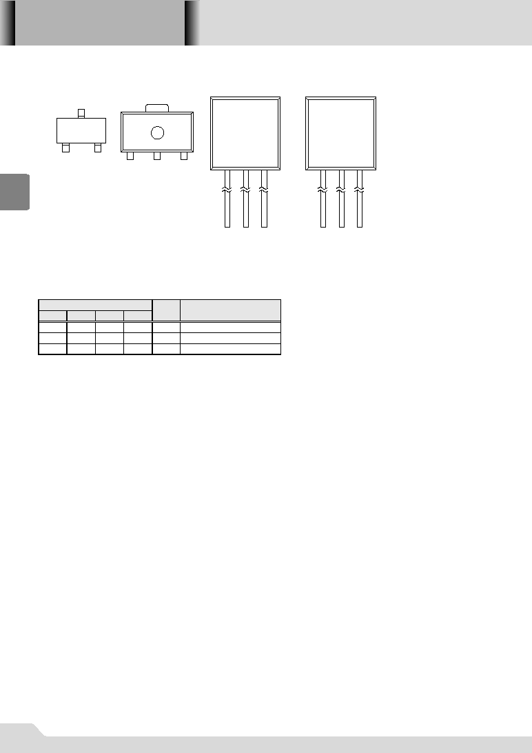
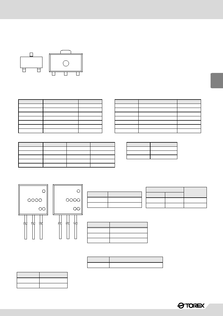
Ultra Small Packages
: SOT-23 (150mW) mini-mold
: SOT-89 (500mW) mini-power mold
: TO-92 (300mW)
* No parts are available with an accuracy of ± 1%
GMicroprocessor reset circuitry
GMemory battery back-up circuits
GPower-on reset circuits
GPower failure detection
GSystem battery life and charge voltage monitors
GDelay circuitry
Features
Applications
NCMOS
NMini Mold Package
NHighly Accurate
: ±2%
NBuilt-In Delay Circuit (1ms ~ 50ms)
(50ms ~ 200ms)
(80ms ~ 400ms)
NLow Power Consumption : 1.0µA (V
IN
= 2.0V)
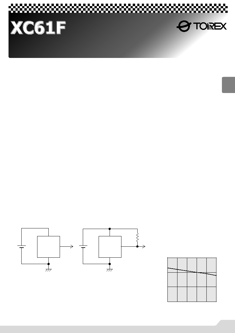
Typical Application Circuits
CMOS output
N-channel open drain output
R
100k
V
IN
V
OUT
V
SS
V
IN
V
OUT
V
SS
V
IN
V
IN
50
100
150
200
-30
-10
10
30
50
70
TDLY
(msec)
Ambient Temp.: Ta()
Typical Performance
Characteristic
AMBIENT TEMPERATURE vs.
TRANSIENT DELAY TIME
02S_04XC61F 02.09.12 14:04 157
XC61F
Series
159
2
Product Classification
GOrdering Information
XC61F
X X X X X X X
a b b c d e f
Output Configuration :
Package Type :
C = CMOS
M = SOT-23
N = N-ch open drain
P = SOT-89
T = TO-92 (Regular)
L = TO-92 (Custom pin
Configuration)
Detect Voltage (V
DF
) :
25 = 2.5V
38 = 3.8V
Output Delay :
Device Orientation :
1 = 50ms to 200ms
R = Embossed Tape ( Right )
4 = 80ms to 400ms
L = Embossed Tape ( Left )
H: Paper Tape (TO-92)
B: Bag (TO-92)
5 = 1ms to 50ms
Detect Accuracy :
2 =
within ± 2.0%
e
f
DESCRIPTION
DESIGNATOR
DESCRIPTION
DESIGNATOR
a
b
c
d
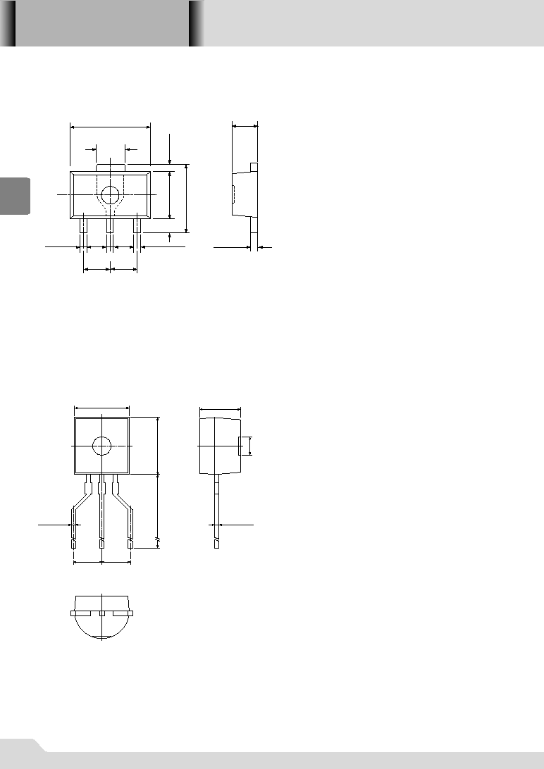
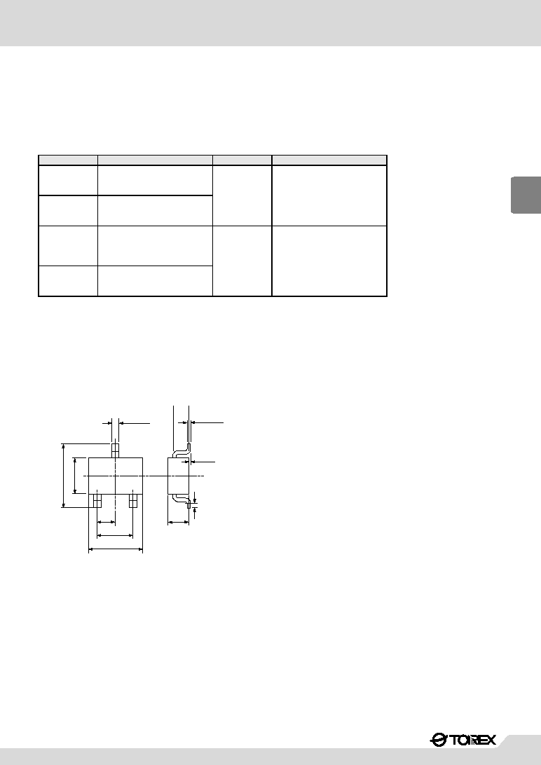
Packaging Information
GSOT-23
1.1±0.1
00.1
0.15
0.95
1.9±0.2
2.9±0.2
0.2min
2.8±0.2
+0.1
-0.05
0.4
+0.1
-0.05
1.6
+0.2
-0.1
02S_04XC61F 02.09.12 14:04 159
XC61F
Series
161
2
Marking
GSOT-23, SOT-89
SOT-23
(TOP VIEW)
SOT-89
(TOP VIEW)
q w e r
q
w
e
r
q Represents the integer of the Detect Voltage and the Output Configuration
CMOS output (XC61FC series)
N-channel open drain (XC61FN series)
VOLTAGE (V)
CMOS
N-ch
CMOS
N-ch
CMOS
N-ch
CMOS
N-ch
CMOS
N-ch
CMOS
N-ch
CMOS
N-ch
w Represents the decimal number of the Detect Voltage
e Indicates the presence of delay time
r Represents the assembly lot no.
Based on internal standards
6
80 to 400ms
7
1 to 50ms
H
DESIGNATOR
CONFIGURATION
A
B
VOLTAGE (V)
K
L
S
M
C
D
E
F
0.
w
1.
w
0.
w
1.
w
CONFIGURATION
DESIGNATOR
2.
w
2.
w
3.
w
4.
w
N
P
3.
w
4.
w
5.
w
6.
w
5.
w
6.
w
R
DESIGNATOR
0
1
q
.4
3
4
2
q
.0
q
.1
q
.2
DESIGNATOR
5
6
7
8
9
VOLTAGE (V)
q
.7
q
.3
q
.8
q
.9
VOLTAGE (V)
q
.5
q
.6
DESIGNATOR
50 to 200ms
5
DELAY TIME
GTO-92
2 3 4 5
6 7
1
TO-92L Type
(TOP VIEW)
61C
L
2 3 4 5
6 7
1
TO-92T Type
(TOP VIEW)
61C
q Represents the output
configuration
DESIGNATOR OUTPUT CONFIGURATION
C
CMOS
N
N-ch
w Re
w
3
5
D
r Indicates Delay Time
DESIGNATOR
DELAY TIME
1
50ms200ms
5
1ms50ms
4
80ms400ms
DESIGNATOR
DETECT VOLTAGE ACCURACY
2
within
±2%
t Represents the Detect Voltage Accuracy
w Represents the Detect Voltage
w
3
3.3
5
5.0
e
DESIGNATOR
VOLTAGEV
3
0
y Represents a least significant digit of
the produced year
DESIGNATOR PRODUCED YEAR
0
2000
1
2001
u Denotes the production lot number
0 to 9, A to Z repeated(G.I.J.O.Q.W excepted)
02S_04XC61F 02.09.12 14:04 161