 | ÐлекÑÑоннÑй компоненÑ: XC61G | СкаÑаÑÑ:  PDF PDF  ZIP ZIP |
Äîêóìåíòàöèÿ è îïèñàíèÿ www.docs.chipfind.ru
101
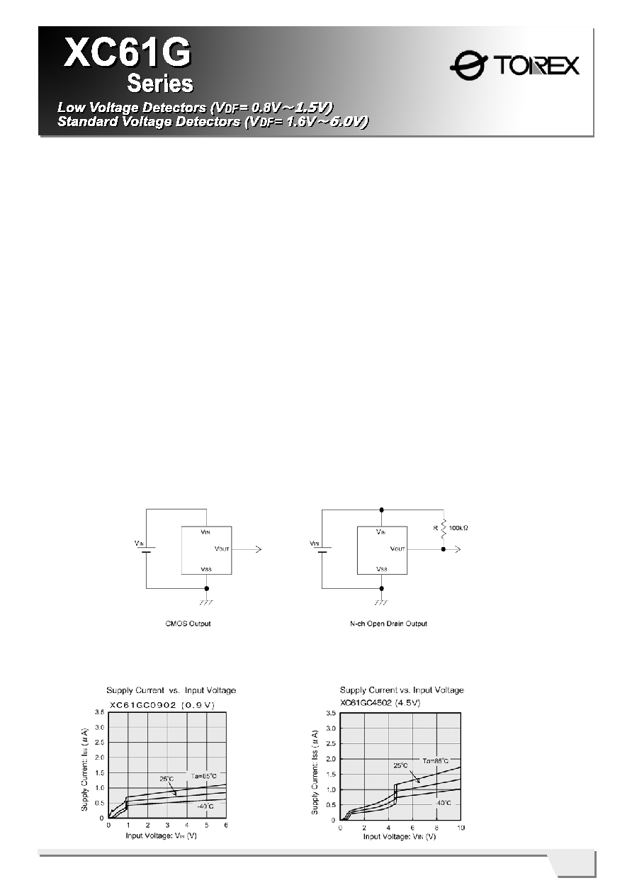
CMOS
Highly Accurate
: ±2%
Low Power Consumption : 0.7A
(V
IN
= 1.5V)
Ultra Small Package
: USP-3
GENERAL DESCRIPTION
The XC61G series are highly precise, low power
consumption voltage detectors, manufactured using CMOS
and laser trimming technologies.
Detect voltage is extremely accurate with minimal
temperature drift.
Both CMOS and N-channel open drain output
configurations are available.
APPLICATIONS
Microprocessor reset circuitry
Memory battery back-up circuits
Power-on reset circuits
Power failure detection
System battery life and charge voltage monitors
TYPICAL PERFORMANCE CHARACTERISTICS
FEATURES
Highly Accurate :
±2%
Low Power Consumption : 0.7 A [ V
IN
=1.5V ] (TYP.)
Detect Voltage Range
: 0.8V ~ 1.5V in 100mV
increments(Low
Voltage)
:
1.6V6.0V in 100mV
increments(Standard
Voltage)
Operating Voltage Range : 0.7V ~ 6.0V(Low Voltage)
:
0.7V10.0V(Standard Voltage)
Detect Voltage Temperature characteristics
:
±100ppm/ (TYP.)
Output Configuration
: N-channel open drain or CMOS
Ultra Small Package :
USP-3(120mW)
TYPICAL APPLICATION CIRCUITS
102
XC61G
Series
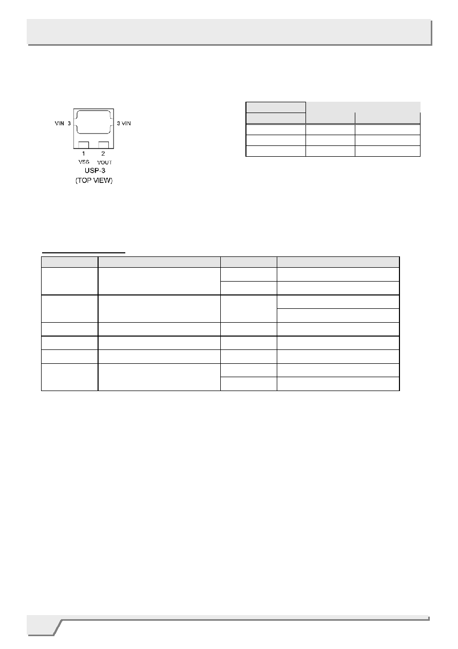
PIN NUMBER
USP-3
PIN NAME
FUNCTION
3 V
IN
Supply Voltage
1 V
SS
Ground
2 V
OUT
Output
DESIGNATOR
DESCRIPTION
SYMBOL
DESCRIPTION
C
: CMOS output
Output Configuration
N
: N-ch open drain output
: e.g. 0.9V 0, 9
Detect Voltage
08 ~ 60
: e.g. 1.5V 1, 5
Output Delay
0
: No delay
Detect Accuracy
2
: Within ± 2%
Package H
:
USP-3
R
: Embossed tape, Standard feed
Device Orientation
L
: Embossed tape, Reverse feed
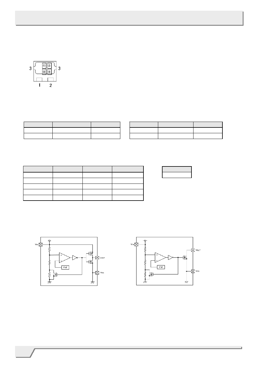
PIN CONFIGURATION
PIN ASSIGNMENT
PRODUCT CLASSIFICATION
Ordering Information
XC61G
103
XC61G
Series
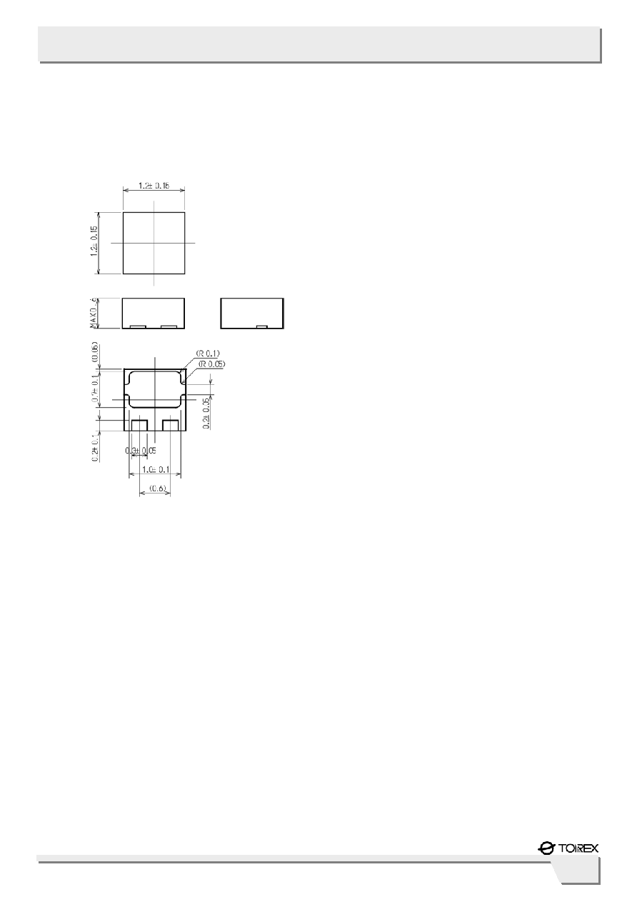
PACKAGING INFORMATION
USP-3
104
XC61G
Series
CMOS Output (XC61GC series)
N-Channel Open Drain Output (XC61GN series)
MARK
CONFIGURATION
VOLTAGE(V)
DESIGNATOR CONFIGURATION VOLTAGE(V)
A CMOS 0.X
K N-ch 0.X
B CMOS 1.X
L N-ch 1.X
MARK
VOLTAGE (V) DESIGNATOR VOLTAGE (V)
0 X.0 5 X.5
1 X.1 6 X.6
2 X.2 7 X.7
3 X.3 8 X.8
4 X.4 9 X.9
MARK
3
MARKING RULE
USP-3
BLOCK DIAGRAMS
Represents integer of output voltage and detect voltage
Represents decimal number of detect voltage
Based on internal standards
( SSOT-24 excepted )
Represents production lot number
0 to 9, A to Z repeated
(G,I,J,O,Q,W excepted)
(1)CMOS Output
(2)N-ch Open Drain Output
USP-3
TOP VIEW
105
XC61G
Series
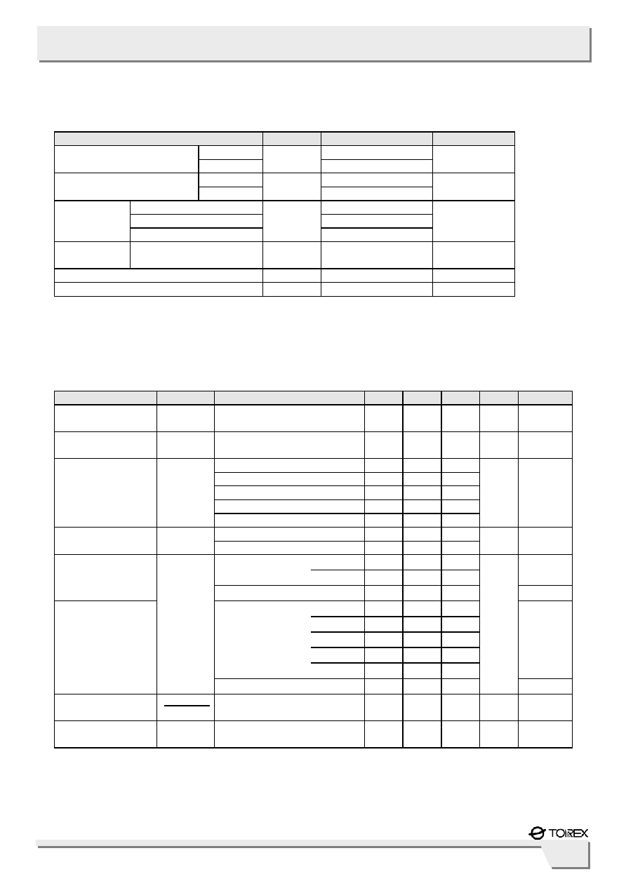
PARAMETER
SYMBOL
RATINGS
UNITS
*1 9.0
Input Voltage
*2
V
IN
12.0
V
*1 50
Output Current
*2
I
OUT
50
mA
CMOS V
SS
-0.3 ~ V
IN
+0.3
N-ch Open Drain Output *1
V
SS
-0.3 ~ 9.0
Output Voltage
N-ch Open Drain Output *2
V
OUT
V
SS
-0.3 ~ 12.0
V
Power
Dissipation
USP-3 Pd 120 mW
Operating Temperature Range
Topr
-40+85
Strage Temperature Range
Tstg
-40+125
PARAMETER
SYMBOL
CONDITIONS
MIN.
TYP.
MAX. UNITS
CIRCUITS
Detect Voltage
V
DF
V
DF
x 0.98
V
DF
V
DF
x 1.02
V 1
Hysteresis Range
V
HYS
V
DF
x 0.02
V
DF
x 0.05
V
DF
x 0.08
V 1
VIN = 1.5V
- 0.7 2.3
= 2.0V
-
0.8
2.7
= 3.0V
-
0.9
3.0
= 4.0V
-
1.0
3.2
Supply Current
I
SS
= 5.0V
-
1.1
3.6
A
2
V
DF
(T) = 0.9V to 1.5V
0.7
-
6.0
Operating Voltage
V
IN
V
DF
(T) = 1.6V to 6.0V
0.7
-
10.0
V 1
VIN =0.7V
0.10
0.80
-
N-ch, VDS = 0.5V
VIN =1.0V
0.85
2.70
-
3
Output Current
(Low Voltage)
CMOS, P-ch, VDS=2.1V VIN =6.0V
-
-7.5
-1.5
4
VIN =1.0V
1.0
2.2
-
VIN =2.0V
3.0
7.7
-
VIN =3.0V
5. 0
10.1
-
VIN =4.0V
6.0
11.5
-
N-ch, VDS = 0.5V
VIN =5.0V
7.0
13.0
-
3
Output Current
(Standard Voltage)
I
OUT
CMOS, P-ch, VDS=2.1V VIN =8.0V
-
-10.0
-2.0
mA
4
Temperature
Characteristics
V
DF
ToprV
DF
-40 Topr 85
-
±100
-
ppm/
-
Delay Time
(VDR VOUT inversion)
tDLY
-
- 0.2 ms
5
ABSOLUTE MAXIMUM RATINGS
Ta = 25
ELECTRICAL CHARACTERISTICS
V
DF
(T) = 0.9 to 1.5V ± 2%
NOTE :
V
DF
(T) : Setting detect voltage
Release Voltage : V
DR
= V
DF
+ V
HYS
Ta=25
*1 Low voltage
*2 Standard voltage