(Can be used with low ESR Capacitor Compatible. ON-OFF Switch) High Speed LDO Regulators
Series
257
3
The XC6204 series are highly precise, low noise, positive voltage LDO
regulators manufactured using CMOS processes. The series achieves
high ripple rejection and low dropout and consists of a standard voltage
source, an error correction, current limiter and a phase compensation
circuit plus a driver transistor.
Output voltage is selectable in 50mV increments within a range of 1.8V ~
6.0V.
The series is also compatible with low ESR ceramic capacitors which
give added output stability. This stability can be maintained even during
load fluctuations due to the excellent transient response of the series.
The current limiter's foldback circuit also operates as a short protect for
the output current limiter and the output pin.
The CE function enables the output to be turned off, resulting in greatly
reduced power consumption.
General Description
Maximum Output Current
: 150mA
Dropout Voltage
: 200mV (I
OUT
= 100mA)
Maximum Operating Voltage : 10V
Output Voltage Range
: 1.8V ~ 6.0V in 50mV increments
Highly Accurate
: � 2%
Low Power Consumption
: TYP 70
�A
Standby Current
: less than 0.1
�A
High Ripple Rejection
: 70dB (10 kHz)
Low Output Noise
: 30
�Vrms
Operational Temperature Range
: -40�C ~ +85�C
Low ESR Capacitor Compatible
: Ceramic capacitor
GMobile phones
GCordless phones
GCameras, video recorders
GPortable games
GPortable AV equipment
GReference voltage
GBattery powered equipment
Features
Applications
NCMOS Low Power Consumption
NDropout Voltage
: 60mV @ 30mA,
200mV @ 100mA
NMaximum Output Current
: 150mA
NHighly Accurate
: � 2%
NOutput Voltage Range : 1.8V ~ 6.0V
NLow ESR capacitor compatible
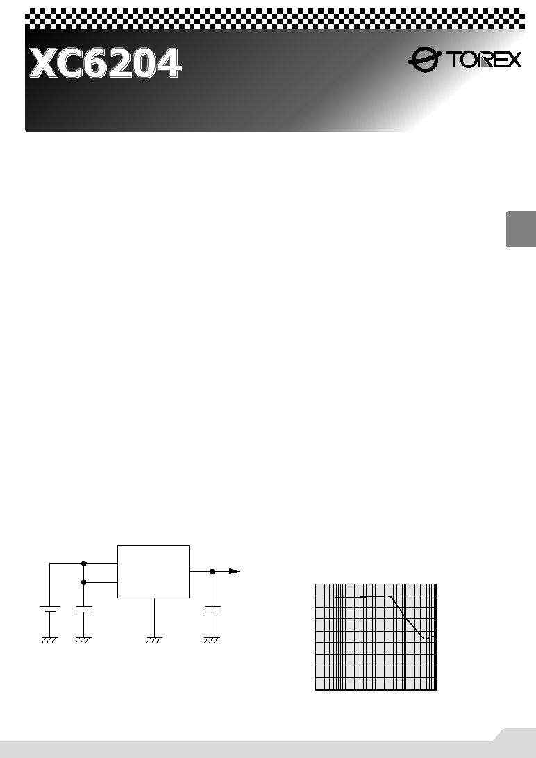
XC6204x302
V
IN
=4.0V
DC
+0.5Vp-p
AC
I
OUT
=50mA, C
L
=1.0
�F(ceramic)
0
60
50
30
40
20
10
80
70
90
Ripple Rejection Rate:RR (dB)
Ripple Frequency:f (kHz)
0.1
1
10
100
1000
V
OUT
V
IN
V
SS
CE
1
�F
C
L
0.1
�F
C
IN
Typical Application Circuit
Typical Performance
Characteristic
03S_04XC6204 02.9.12 2:57 PM 257
Product Classification
GSelection Guide
The following options for the CE pin logic and internal pull-up/down are available:
Active 'High' + no pull-down resistor built-in (standard)
Active 'High' + 300k
pull-down resistor built-in <between CE-V
SS
> (semi-custom)
Active 'Low' + no pull-up resistor built-in (semi-custom)
Active 'Low' + 300k
pull-up resistor built-in <between CE-V
SS
> (semi-custom)
Note: *With the pull-up resistor or pull-down resistor built-in types, the supply current during operation will increase by V
IN
/ 300k
(TYP.)
XC6204
Series
258
3
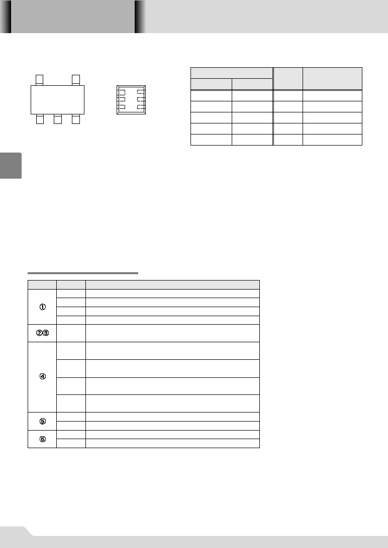
Pin Configuration
Pin Assignment
5
V
OUT
NC
V
IN
V
SS
SOT-25
USP-6B
CE
4
3
2
1
V
IN
1
NC 2
V
OUT
3
6 CE
4 NC
5 V
SS
TOP VIEW
PIN NUMBER
SOT-25
USP-6B
1
2
3
1
5
6
PIN NAME
FUNCTION
V
IN
V
SS
CE
5
3
V
OUT
Input
Ground
ON/OFF Control
Output
4
24
NC
No Connection
GOrdering Information
DESIGNATOR
A
B
C
D
2
A
M
D
R
L
1816
Active 'High' (pull-down resistor built in)
Active 'High' (no pull-down resistor built in)
Active 'Low' (pull-up resistor built in)
Active 'Low' (no pull-up resistor built in)
Output Voltage :
e.g. 20 = 2.0V, 30 = 3.0V etc.
Output Voltage : 100mV increments,
� 2% accuracy
e.g. w=3, e=8, r=2 3.8V,
� 2%
1
(Note1)
Output Voltage : 100mV increments,
� 1% accuracy
e.g. w=3, e=0, r=1 3.0V,
� 1%
USP-6B
SOT-25
Embossed Tape : Standard Feed
Embossed Tape : Reverse Feed
Output Voltage : 50mV increments,
� 2% accuracy
e.g. w=3, e=8, r=A 3.85V
B
(Note1)
Output Voltage : 50mV increments,
� 1% accuracy
e.g. w=3, e=0, r=B 3.05V,
� 1%
SYMBOL
DESCRIPTION
XC6204 qwerty
Please note that the "B" version is the standard part. The A, C, & D versions are semi-custom parts.
Note 1 : The output voltage range of the
�1% accuracy product is 3.0V 6.0V.
03S_04XC6204 02.9.12 2:57 PM 258
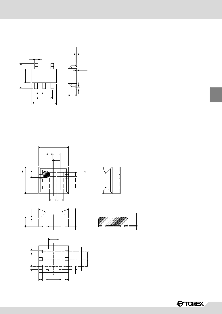
Packaging Information
GSOT-25
A'
A
2.0�0.15
0.5�0.1
0.005�
0.002
(0.45)
(0.45)
(0.45)
(0.05)
AAA
A
A
A
(0.45)
0.65
0.125
+0.15
- 0.05
0.05
+0.01
- 0.005
(0.27)
(0.27)
(0.27)
1.8�
0.15
45
45
6
5
4
1
2
3
45
45
Note : Pin 1 is larger than the other pins.
A-A' cross section
1.0�0.1
0.7�0.03
0.25�0.1
0.25�0.1
0.2�0.05
5-0.2�0.05
0.5�0.1
0.1�0.03
0.5�0.1
1.6�0.1
3
2
1
4
5
6
GUSP-6B
0.4
0.95
1.9�0.2
2.9�0.2
+0.1
-0.05
1.1�0.1
00.1
0.15
0.2min
+0.1
-0.05
2.8�0.2
1.6
+0.2
-0.1
XC6204
Series
259
3
03S_04XC6204 02.9.12 2:57 PM 259

XC6204
Series
260
3
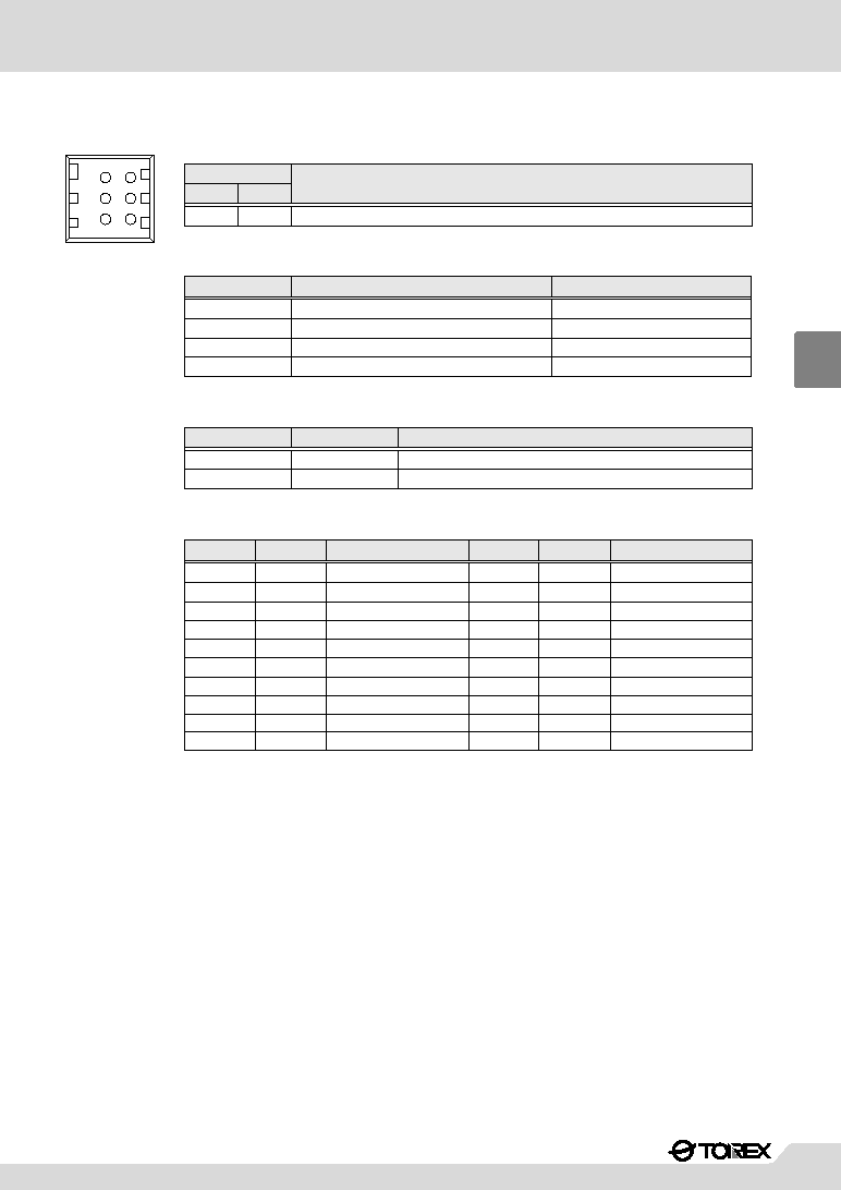
Marking
GSOT-25
DESIGNATOR
PRODUCT NAME
4
XC6204M
q Represents the product name
w Represents the type of regulator
Voltage =0.13.0V
V
Voltage=3.16.0V
Voltage=3.156.05V
DESIGNATOR
XC6204AM
XC6204DM
PRODUCT NAME
L
P
Voltage=0.153.05V
E
K
Output Voltage 100mV step
Output Voltage 50mV step
A
D
Z
XC6204CM
N
H
C
Y
XC6204BM
M
F
B
X
r Denotes the production lot number
0 to 9, A to Z repeated(G.I.J.O.Q.W excepted)
e Represents the output voltage
0
E
DESIGNATOR
4
3
2
1
D
C
B
A
9
8
7
6
5
Output VoltageV
F
Z
DESIGNATOR
M
L
K
H
Y
X
V
U
T
S
R
P
N
1.6
3.0
2.0
1.9
1.8
1.7
2.9
2.8
2.7
2.6
2.5
2.4
2.3
2.2
2.1
4.6
6.0
5.9
5.8
5.7
5.6
5.5
5.4
5.3
5.2
5.1
5.0
4.9
4.8
4.7
Output VoltageV
-
-
-
-
-
-
3.1
4.5
-
4.4
-
4.3
-
4.2
-
4.1
-
4.0
-
3.9
-
3.8
-
3.7
-
3.6
3.5
3.4
3.3
3.2
-
-
-
-
-
-
3.15
4.55
-
4.45
-
4.35
-
4.25
-
4.15
-
4.05
-
3.95
-
3.85
-
3.75
-
3.65
3.55
3.45
3.35
3.25
1.65
3.05
2.05
1.95
1.85
1.75
2.95
2.85
2.75
2.65
2.55
2.45
2.35
2.25
2.15
4.65
6.05
5.95
5.85
5.75
5.65
5.55
5.45
5.35
5.25
5.15
5.05
4.95
4.85
4.75
SOT-25
(TOP VIEW)
q w e r
03S_04XC6204 02.9.12 2:57 PM 260
XC6204
Series
261
3
qw Represents the product name
e Represents the type of regulator
q
0
w
DESIGNATOR
XC6204D
PRODUCT NAME
4
PRODUCT NAME
XC6204DD
Type
CE pin, Active 'High' no pull-up resistor built in
DESIGNATOR
D
XC6204CD
CE pin, Active 'High' pull-up resistor built in
C
XC6204BD
CE pin, Active 'High' no pull-down resistor built in
B
XC6204AD
CE pin, Active 'High' pull-down resistor built in
A
r Represents the integer of the Output Voltage
3
DESIGNATOR
XC62043D
XC62045D
PRODUCT NAME
3.X
5.X
VOLTAGEV
5
4
5
6
1
2
3
USP6B
(TOP VIEW)
y Denotes the production lot number
0 to 9, A to Z repeated(G.I.J.O.Q.W excepted)
Note : Character inversion is not used.
t Represents the decimal number of Output Voltage
DESIGNATOR
X.1
4
X.5
3
X.4
2
X.3
1
X.2
VOLTAGEV
9
8
X.9
7
X.8
6
X.7
5
X.6
PRODUCT NAME
XC62041D
XC62045D
XC62044D
XC62043D
XC62042D
XC62049D
XC62048D
XC62047D
XC62046D
B
DESIGNATOR
F
E
D
C
VOLTAGEV
M
L
K
H
PRODUCT NAME
XC62041AD
X.0
X.15
X.55
X.45
X.35
X.25
X.95
X.85
X.75
X.65
X.05
0
XC62040D
A
XC62040AD
XC62049AD
XC62048AD
XC62047AD
XC62046AD
XC62045AD
XC62044AD
XC62043AD
XC62042AD
GUSP-6B
03S_04XC6204 02.9.12 2:57 PM 261