CMOS Low Power Consumption
Applications
Dropout Voltage :
Mobile phones
60mV @ 30mA, 200mV @ 100mA
Cordless phones
Maximum Output Current : 300mA
Cameras, video recorders
300mA (VOUT
2.0V, VIN=VOUT+1V)
Portable games
(VOUT<2.0V, VIN=3.0V)
Portable AV equipment
Highly Accurate :
±
2% (
±
1% as semi-custom)
Reference voltage
Output Voltage Range : 1.8V
~
6.0V
Battery powered equipment
Low ESR capacitor compatible
General Description
Features
Maximum Output Current : 300mA (E to H Series)
(VOUT
2.0V, VIN=VOUT+1V)
(VOUT<2.0V, VIN=3.0V)
Dropout Voltage : 200mV (I
OUT
= 100mA)
Maximum Operating Voltage : 10V
Output Voltage Range : 1.8V ~ 6.0V in 50mV increments
Highly Accurate :
±
2%, (
±
1% as semi-custom)
Low Power Consumption : TYP 70
µ
A
Standby Current : less than 0.1
µ
A
High Ripple Rejection : 70dB (10 kHz)
Low Output Noise : 30
µ
Vrms
Operating Temperature Range : -40
O
C ~ +85
O
C
Low ESR Capacitor Compatible : Ceramic capacitor
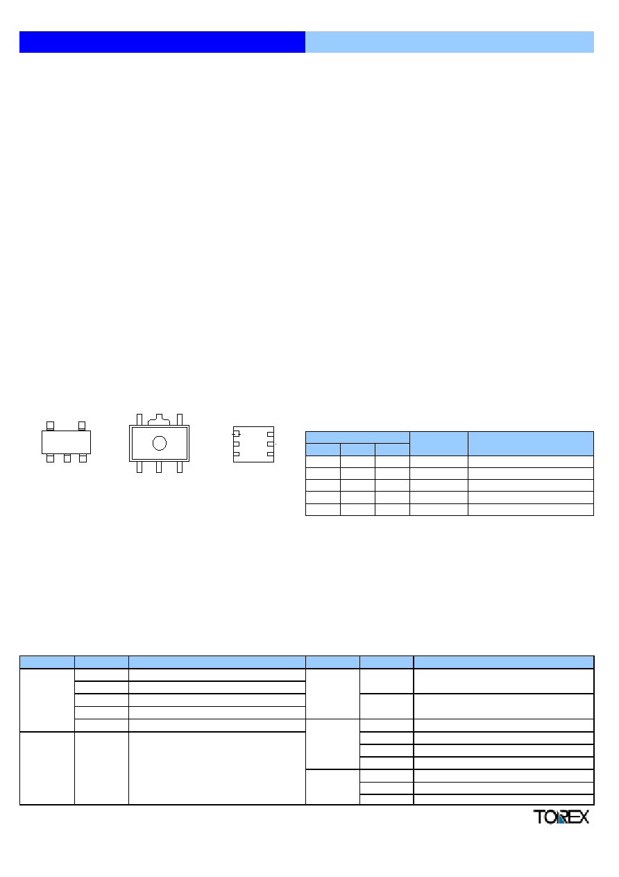
Pin Configuration
Pin Assignment
Selection Guide
The following options for the CE pin logic and internal pull-up/down are available:
Active 'High' + no pull-down resistor built-in (standard)
Active 'High' + 300k
pull-down resistor built-in <between CE-VSS> (semi-custom)
Active 'Low' + no pull-up resistor built-in (semi-custom)
Active 'Low' + 300k
pull-up resistor built-in <between VIN-CE> (semi-custom)
Note: *With the pull-up resistor or pull-down resistor built-in types, the supply current during operation will increase by VIN / 300k
(TYP.)
Ordering Information
XC6204
123456
DESIGNATOR
SYMBOL
DESIGNATOR
SYMBOL
Output Voltage: 100mV increments,
±
2% accuracy
E
Active 'High' (pull-down resistor built in)
e.g.
2
=2,
3
=8,
4
=2
2.80V
F
Active 'High' (no pull-down resistor built in)
Output Voltage : 50mV increments, ±2% accuracy
G
Active 'Low' (pull-up resistor built in)
e.g.
2
=2,
3
=8,
4
=A
2.85V
H
Active 'Low' (no pull-up resistor built in)
Output Voltage :
M
e.g.
2
=3,
3
=0
3.0V
P
SOT-89
D
R
L
Feb. 7, 2003 Ver. 2
DESCRIPTION
Preliminary
High Speed LDO Regulators
Output On/Off Control
XC6204E, F, G, H Series
SOT-25 (SOT-23-5)
DESCRIPTION
CE Pin Logic :
Package Type :
USP - 6B
Embossed Tape : Standard Feed
Embossed Tape : Reverse Feed
Device Orientation :
2 3
Integer
4
2
1
6
A
5
6
5
4
1
2
3
VIN
NC
VOUT
CE
VSS
NC
USP-6B
[TOP VIEW]
4
2
5
1
3
CE
(NC)
V
IN
V
SS
V
OUT
SOT-25
(SOT-23-5)
[TOP VIEW]
The XC6204 series are highly accurate, low noise, CMOS LDO Voltage
Regulators. Offering low output noise, high ripple rejection ratio, low dropout and
very fast turn-on times, the XC6204 series is ideal for today's cutting edge mobile
phone and Bluetooth applications.
Internally the XC6204 includes a reference voltage source, error amplifiers, driver
transistors, current limiters and phase compensators. The XC6204's current
limiters' foldback circuit also operates as a short protect for the output current
limiter.
The output voltage for each regulator is set independently, by laser trimming.
Voltages are selectable in 50mV steps within a range of 1.8V to 6.0V. The XC6204
series is also fully compatible with low ESR ceramic capacitors, reducing cost and
improving output stability. This high level of output stability is maintained even
during frequent load fluctuations, due to the excellent transient response
performance and high PSRR achieved across a broad range of frequencies.
The CE function allows the output of each regulator to be turned off independently,
resulting in greatly reduced power consumption.
The XC6204 series is available in the SOT-25, SOT-89 or USP-6B `chip-scale'
package. Measuring only 2.0mm x 1.8mm the USP-6B is perfect for applications
where PCB area is critical.
VOUT
5
VSS
2
VIN
4
1
NC
2
VSS
3
CE
PIN NUMBER
SOT-25 SOT-89 USP-6B
1
2
3
4
5
4
2
3
1
5
1
5
6
2, 4
3
PIN NAME
VIN
VSS
CE
NC
VOUT
FUNCTION
Input
Ground
ON/OFF Control
No Connection
Output
SOT-89
[TOP VIEW]
1
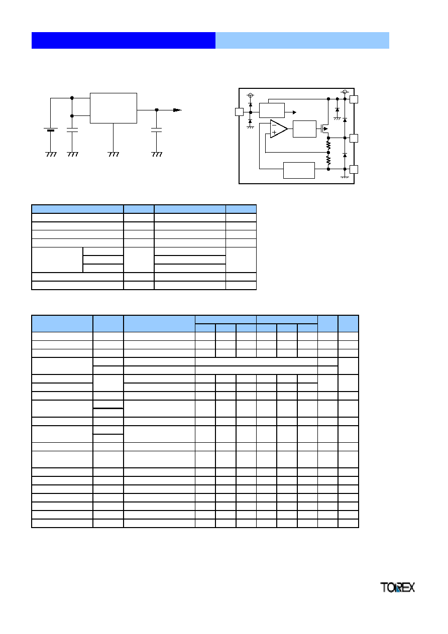
Typical Application
Block Diagram
Absolute Maximum Ratings
* IOUT=Pd / Range of (VIN-VOUT)
Electrical Characteristics XC6204E, F Series
Note
* 300mA (VOUT
2.0V, VIN=VOUT+1V)
(NOTE 1) Unless otherwise stated, V
IN
=V
OUT
(T)+1.0V
(VOUT<2.0V, VIN=3.0V)
(NOTE 2) V
OUT
(T)=Specified Output Voltage
(NOTE 4) Vdif={VIN1
(NOTE6)
-V
OUT
1
(NOTE5)
}
(NOTE 5) V
OUT
1=A voltage equal to 98% of the Output Voltage whenever an amply stabilized I
OUT
{V
OUT
(T)+1.0V} is input.
(NOTE 6) V
IN
1=The Input Voltage when V
OUT
1 appears as Input Voltage is gradually decreased.
(NOTE 7) The values for -40
O
C
Ta
85
O
C are designed values.
2
500
Preliminary
Storage Temperature
100
-40 ~ +85
Operating Ambient Temperature
Power Dissipation
Output On/Off Control
Feb. 7, 2003 Ver. 2
RATINGS
12
500
V
SS
-0.3 ~ V
IN
+0.3
V
SS
-0.3 ~ V
IN
+0.3
250
SOT-23-5
USP-6B
PARAMETER
Input Voltage
Output Current
Output Voltage
SOT-89
VIN=[VOUT(T)+1.0]V+1.0Vp-pAC
I
OUT
=50mA, f=10kHz
V
IN
=VCE=V
OUT
(T)+1.0V
V
IN
=VCE=V
OUT
(T)+1.0V
V
IN
=V
OUT
(T)+1.0V, V
CE
=V
IN
V
IN
=V
OUT
(T)+1.0V, V
CE
=V
IN
V
CEL
I
CEH
I
CEH
I
CEL
0.05
1.00
40
70
0.01
0.10
50
90
145
80
120
×
0.97
V
OUT
(T)
×
1.03
E-1
300
15
50
300
-40
O
C
Ta
85
O
C
MIN
TYP
MAX
MAX
V
OUT
(T)
×
1.02
PARAMETER
Ta=25
O
C
SYMBOL
CONDITIONS
TYP
Istby
VIN=VOUT(T)+1.0V, VCE=VSS
V
OUT
(T)+1.0V
V
IN
10V
I
OUT
=30mA
V
OUT
VIN
VOUT
Ishort
V
CEH
V
OUT
Topr
VOUT
en
PSRR
Ilim
V
IN
I
OUT
=30mA
Temp. Characteristics
-40
O
C
Topr
85
O
C
Output Noise
Ripple Rejection Rate
CE "High" Current ( E series)
Current Limiter
Short-circuit Current
CE "High" Voltage
CE "Low" Voltage
Standby Current
Line Regulation
Input Voltage
Output Voltage
Supply Current (F series)
Supply Current (E series)
I
DD
I
OUT
=30mA
I
OUT
=100mA
V
IN
=V
CE
=V
OUT
(T)+1.0V
VIN=VCE=V
OUT
(T)+1.0V
V
mW
O
C
O
C
Output Voltage
Maximum Output Current
×
0.98
V
OUT
(E)
IOUTMAX
I
OUT
=30mA
30
1mA
I
OUT
100mA
100
10
50
80
120
I
OUT
=10mA, 300Hz~50kHz
mV
0.05
0.30
30
80
40
E-2
µ
A
µ
A
Load Regulation
Dropout Voltage
V
OUT
Vdif1
Vdif2
* 1
SYMBOL
V
IN
I
OUT
V
OUT
V
CE
Topr
Tstg
-55 ~ +125
Pd
2
0.01
0.20
10
100
2
70
380
380
60
50
1.6
VIN
VIN
1.7
0.25
-0.1
-0.1
20
0.10
-0.15
0.20
25
0.15
0.15
0.10
-0.15
-0.15
XC6204E, F, G, H Series
High Speed LDO Regulators
UNITS
CIRCUIT
CE Input Voltage
MIN
UNITS
V
mA
V
V
mA
mV
mV
% / V
V
ppm /
O
C
µ
Vrms
dB
mA
mA
V
V
µ
A
2
2
1
-
1
3
4
1
1
1
1
1
1
1
1
2
2
2
(NOTE 3) V
OUT(E)
=Effective Output Voltage (I.e. the output voltage when "V
OUT(T)
+1.0V" is provided at the V
IN
pin while maintaining a certain I
OUT
value).
µ
A
µ
A
CE "Low" Current
CE "High" Current (F series)
-0.1
V
IN
=V
OUT
(T)+1.0V, V
CE
=V
SS
VIN
CE
VSS
VOUT
V
SS
V
OUT
V
IN
Current
Limiter
ON/OFF
Control
Voltage
Reference
each
circuit
CE
R2
R1
CIN
0.1
µ
F
CL
1
µ
F
* The Diode in the circuit is the protective Diode.
Electrical Characteristics XC6204G, H Series
* 300mA (VOUT
2.0V, VIN=VOUT+1V)
Note
(VOUT<2.0V, VIN=3.0V)
(NOTE 1) Unless otherwise stated, V
IN
=V
OUT
(T)+1.0V
(NOTE 2) V
OUT
(T)=Specified Output Voltage
(NOTE 4) Vdif={VIN1
(NOTE6)
-V
OUT
1
(NOTE5)
}
(NOTE 5) V
OUT
1=A voltage equal to 98% of the Output Voltage whenever an amply stabilized I
OUT
{V
OUT
(T)+1.0V} is input.
(NOTE 6) V
IN1
=The Input Voltage when V
OUT1
appears as Input Voltage is gradually decreased.
(NOTE 7) The values for -40
O
C
Ta
85
O
C are designed values.
3
Preliminary
XC6204E, F, G, H Series
Feb. 7, 2003 Ver. 2
×
1.02
×
0.97
V
OUT
(T)
V
OUT
(T)
High Speed LDO Regulators
Output On/Off Control
-40
O
C
Ta
85
O
C
UNITS
CIRCUIT
MIN
TYP
MAX
×
1.03
PARAMETER
SYMBOL
CONDITIONS
Ta=25
O
C
MIN
TYP
MAX
Output Voltage
V
OUT
(E)
I
OUT
=30mA
×
0.98
V
1
Maximum Output Current
IOUTMAX
*1
300
300
mA
1
Load Regulation
V
OUT
1mA
I
OUT
100mA
15
50
30
80
mV
1
Dropout Voltage
Vdif1
I
OUT
=30mA
E-1
mV
1
Vdif2
I
OUT
=100mA
E-2
mV
Supply Current (G series)
I
DD
V
IN
=V
OUT
(T)+1.0V, V
CE
=V
SS
50
80
120
50
90
145
µ
A
2
Supply Current (H series)
V
IN
=V
OUT
(T)+1.0V, V
CE
=V
SS
40
70
100
40
80
120
Standby Current
Istby
V
IN
=VCE=V
OUT
(T)+1.0V
0.01
0.10
0.05
1.00
µ
A
2
Line Regulation
V
OUT
V
OUT
(T)+1.0V
V
IN
10V
0.01
0.20
0.05
0.30
% / V
1
VIN
VOUT
I
OUT
=30mA
Input Voltage
V
IN
2
10
2
10
V
-
Output Voltage
V
OUT
I
OUT
=30mA
ppm /
O
C
1
Temp. Characteristics
Topr
VOUT
-40
O
C
Topr
85
O
C
100
Output Noise
en
I
OUT
=10mA, 300Hz~50kHz
30
µ
Vrms
3
Ripple Rejection Rate
PSRR
VIN=[VOUT(T)+1.0]V+1.0Vp-pAC
dB
4
I
OUT
=50mA, f=10kHz
70
Current Limiter
Ilim
V
IN
=V
OUT
(T)+1.0V, V
CE
=V
SS
380
380
mA
1
Short-circuit Current
Ishort
V
IN
=V
OUT
(T)+1.0V, V
CE
=V
SS
50
60
mA
1
CE "High" Voltage
V
CEH
1.6
VIN
1.7
VIN
V
1
CE "Low" Voltage
V
CEL
0.25
0.20
V
1
CE "High" Current
I
CEH
V
IN
=VCE=V
OUT
(T)+1.0V
-0.1
0.10
-0.15
CE "Low" Current (G series)
I
CEL
V
IN
=V
OUT
(T)+1.0V, V
CE
=V
SS
-20
µ
A
2
0.15
µ
A
2
-0.1
0.15
0.10
-25
0.15
µ
A
2
(NOTE 3) V
OUT(E)
=Effective Output Voltage (I.e. the output voltage when "V
OUT(T)
+1.0V" is provided at the V
IN
pin while maintaining a certain I
OUT
value).
0.10
-0.15
CE "Low" Current (H series)
I
CEL
V
IN
=V
OUT
(T)+1.0V, V
CE
=V
SS