Preliminary
February 07, 2003 Ver. 2
CMOS Low Power Consumption
70
µ
A
Applications
Maximum Output Current
: 150mA
Mobile phones, Cordless phones
Highly Accurate
:
±
2% (
±
30mV less than 1.5V)
Wireless communication equipment
Output Voltage Range
: 0.9V ~ 1.75V (50mV Step)
Portable games
High Ripple Rejection
: 60dB
Cameras, Video recorders
Low Noise
: 30
µ
Vrms
Portable AV equipment
Low ESR capacitor compatible
Reference voltage
Battery powered equipment
General Description
Features
Maximum Output Current
: 150mA
Maximum Operating Voltage
: 2.0V ~ 10V
Output Voltage Range
: 0.9V~1.75V(50mV Step)
Highly Accurate
:
±
2% (V
OUT
>1.5V)
:
±
30mV (V
OUT
1.5V)
Low Power Consumption
: TYP 70
µ
A
Standby Current
: Less than 0.1
µ
A (TYP)
Low Noise
: 30
µ
Vrms (TYP)
High Ripple Rejection
: 60dB (10kHz)
Operating Temperature Range
: -40
O
C ~ +85
O
C
Low ESR Capacitor Compatible : Ceramic capacitor
Ultra Small Packages
: SOT-25 (SOT-23-5)
SOT-89-5
USP-6B
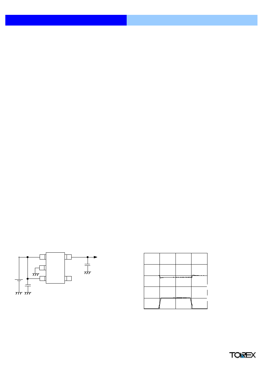
Typical Application
Electrical Characteristics
Load Transient Response
1
XC6205 Series
High Speed LDO Regulators
Low ESR Cap. Compatible, Output On/Off Control
Output Current
Output Voltage
The XC6205 series are highly precise, low noise, positive
voltage LDO regulators manufactured using CMOS processes.
The series achieves high ripple rejection and low dropout and
consists of a voltage reference, an error amplifier, a current
limiter and a phase compensation circuit plus a driver transistor.
Output voltage is selectable in 50mV increments within a range
of 0.9V ~ 1.75V.
The series is also compatible with low ESR ceramic capacitors
which give added output stability. This stability can be
maintained even during load fluctuations due to the excellent
transient response of the series.
The current limiter's foldback circuit also operates as a short
protect for the output current limiter and the output pin.
The CE function enables the output to be turned off, resulting in
greatly reduced power consumption.
V
IN
V
OUT
NC
CE
CL
2.2
µ
F
V
SS
CIN
1
µ
F
5
4
3
2
1
VIN=2V, tr=tf=5
µ
sec
CIN=1
µ
F(ceramic), CL=4.7
µ
F(ceramic)
Output Voltage (V)
250
1.00
Time (40
µ
sec/div)
XC6205B092
0.95
0.90
0.85
0.80
0.75
200
150
100
50
0
Output Current (mA)
50mA
1mA

Preliminary
Pin Assignment
Block Diagram
Pin Configuration
* The diode in the above diagram is for the IC's protection.
Selection Guide
The following options for the CE pin logic and internal pull-up/down are available:
Active 'High' + no pull-down resistor built-in (standard)
Active 'High' + 300M
pull-down resistor built-in <between CE-V
SS
> (semi-custom)
Active 'Low' + no pull-up resistor built-in (semi-custom)
Active 'Low' + 300M
pull-up resistor built-in <between V
IN
-CE> (semi-custom)
Note: *With the pull-up resistor or pull-down resistor built-in types, the supply current during operation will increase
by VIN / 300M
(TYP.).
Ordering Information
XC6205
123456
Output Voltage : 100mV Step
Accuracy : within
±
2%
e.g.
2
=0,
3
=9,
4
=2
0.9V
Output Voltage : 50mV Step
Accuracy : within
±
2%
e.g.
2
=1,
3
=3,
4
=A
1.35V
Package Type : SOT-25(SOT-23-5)
USP - 6B
Output Voltage :
Device Orientation :
e.g. 1.5V =
2
: 1,
3
: 5
Embossed Tape : Standard Feed
Embossed Tape : Reverse Feed
2
6
R
L
2 3
1
A
B
C
D
Integer
D
DESIGNATOR SYMBOL
2
M
Low ESR Cap. Compatible, Output On/Off Control
DESIGNATOR SYMBOL
4
5
DESCRIPTION
Active 'Low'
(no pull-up resistor built in)
XC6205 Series
High Speed LDO Regulators
DESCRIPTION
Active 'High'
(pull-down resistor built in)
Active 'High'
(no pull-down resistor built in)
Active 'Low'
(pull-up resistor built in)
A
VSS
CE
NC
VOUT
Ground
ON/OFF Control
No Connection
Output
PIN NAME
FUNCTION
Input
VIN
5
5
3
PIN NUMBER
SOT-25
SOT-89-5
USP-6B
1
4
3
3
6
4
1
2, 4
1
2
2
5
4
2
5
1
3
CE
(NC)
V
IN
V
SS
V
OUT
6
5
4
1
2
3
VIN
NC
VOUT
CE
VSS
NC
SOT-25 (SOT-23-5)
(TOP VIEW)
USP-6B
(TOP VIEW)
V
SS
V
OUT
V
IN
Current
Limiter
ON/OFF
Control
Voltage
Reference
each circuit
CE
R2
R1
VOUT
5
VSS
2
VIN
4
1
NC
2
VSS
3
CE
SOT-89-5
(TOP VIEW)

Preliminary
Absolute Maximum Rating
Electrical Characteristics
XC6205x152 (1.5V)
Ta=25
O
C
NOTE
(NOTE 1) V
OUT
(T)=Specified Output Voltage
(NOTE 2) V
OUT
(E)=Effective Output Voltage
(I.e. the output voltage when "V
OUT
(T)+1.0V" is provided at the V
IN
pin while maintaining a certain I
OUT
value).
(NOTE 3) Vdif={V
IN
1
(NOTE5)
-V
OUT
1
(NOTE4)
}
(NOTE 4) VOUT 1 = A voltage equal to 98% of the Output Voltage whenever an amply stabilized IOUT {VOUT(T) + 1.0V} is input.
(NOTE 5) V
IN
1=The Input Voltage when V
OUT1
appears as Input Voltage is gradually decreased.
(NOTE 6) Unless otherwise stated, V
IN
=V
OUT
(T)+1.0V
3
UNITS
mA
mV
mV
1.530
V
V
mA
V
XC6205 Series
High Speed LDO Regulators
Low ESR Cap. Compatible, Output On/Off Control
PARAMETER
Input Voltage
RATINGS
V
IN
SYMBOL
V
OUT
12
500
V
SS
-0.3 ~ V
IN
+0.3
I
OUT
1.500
V
OUT
(E)
Topr
Tstg
Operating Ambient Temperature
Storage Temperature
PARAMETER
SYMBOL
250
100
-40 ~ +85
TYP
-55 ~ +125
CONDITIONS
ppm/
O
C
dB
500
µ
A
µ
A
% / V
V
-
100
1
2
1
2.0
2
Output Current
Output Voltage
CE Input Voltage
Pd
Power
Dissipation
SOT-25(SOT-23-5)
USP-6B
V
CE
V
IN
1
1
15
50
0.01
0.10
10.0
I
OUT
=30mA
-40
O
C
Topr
85
O
C
Line Regulation
V
IN
V
OUT
V
OUT /
Temperature Characteristics
V
OUT /
Topr
V
OUT
Output Voltage
Input Voltage
2
30
3
0.10
50
µ
Vrms
mA
V
CE
=V
IN
V
IN
=V
OUT
+1.5V, V
OUT
=V
SS
-0.10
4
300
1
mA
60
0.10
V
IN
µ
A
V
V
µ
A
1
0.25
2
2
Current Limiter
Output Noise
Ilim
I
OUT
=50mA, f=10kHz
Ripple Rejection Rate
PSRR
en
300Hz ~ 50kHz
CE "Low" Current
I
CEL
CE "Low" Voltage
V
CEL
CE "High" Current
I
CEH
Standby Current
Istby
◊
1.02
150
Maximum Output Current
I
OUT
MAX
V
CE
=V
SS
Load Regulation
V
OUT
CIRCUIT
MIN
MAX
UNITS
Output Voltage
Vdif1
Supply Current
I
DD
Dropout Voltage
Vdif2
1.470
1
I
OUT
=30mA
V
mV
1
600
I
OUT
=30mA
I
OUT
=100mA
CE "High" Voltage
V
CEH
1.60
Short-circuit Current
Ishort
V
SS
-0.3 ~ V
IN
+0.3
0.20
V
CE
=V
IN
0.01
70
mW
O
C
V
OUT
(T)+1.0V
V
IN
10V
I
OUT
=30mA
2
O
C
1mA
I
OUT
100mA
V
OUT
(T)
◊
0.98
V
CE
=V
SS
-0.10
Preliminary
!
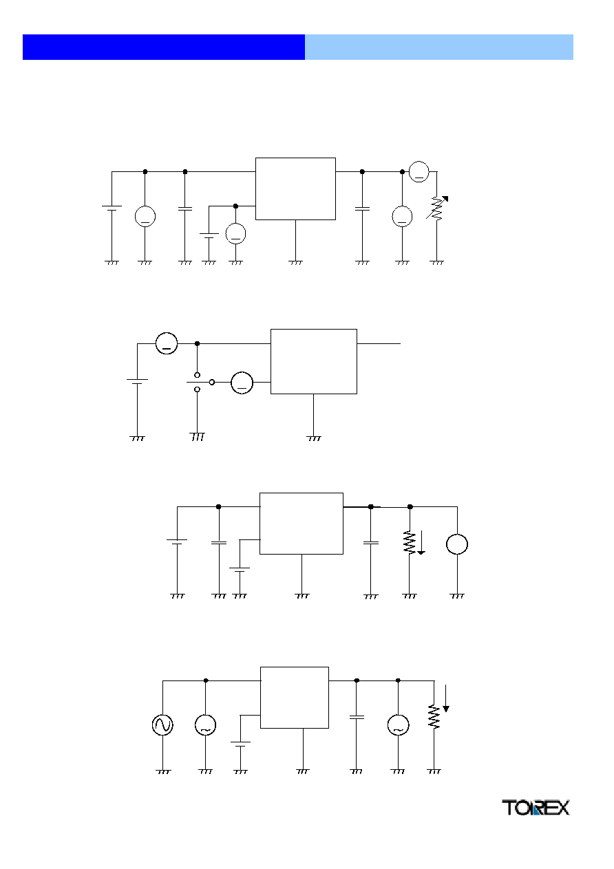
Test Circuits
Circuit 1
Circuit 2
Circuit 3
Circuit 4
4
XC6205 Series
High Speed LDO Regulators
Low ESR Cap. Compatible, Output On/Off Control
CIN=1.0
µ
F
(ceramic)
V
VIN
VOUT
VSS
CE
CL=2.2
µ
F
(ceramic)
RL
A
V
V
VIN
VOUT
VSS
CE
A
OPEN
A
VIN
VOUT
VSS
CE
CIN=1.0
µ
F
(ceramic)
CL=2.2
µ
F
(ceramic)
F.F.T
IOUT=10mA
VIN
VOUT
VSS
CE
V
IOUT=50mA
V
VIN={VOUT+1} V
DC
+0.5V
p-pAC
CL=2.2
µ
F
(ceramic)

Preliminary
!
Operational Explanation
Output voltage control with the XC6205 series :
Low ESR Capacitors
Recommended Output Capacitor Values
Current Limiter, Short-Circuit Protection
CE Pin
5
The XC6205 series includes a combination of a fixed current limiter circuit & a foldback circuit which aid the
operations of the current limiter and circuit protection. When the load current reaches the current limit level, the
fixed current limiter circuit operates and output voltage drops. As a result of this drop in output voltage, the foldback
circuit operates, output voltage drops further and output current decreases. When the output pin is shorted, a
current of about 50mA flows. However, when the input/output voltage differential is quite small, this current will be
about 200mA.
XC6205 Series
High Speed LDO Regulators
Low ESR Cap. Compatible, Output On/Off Control
0.9V ~ 1.2V
1.25V ~ 1.75V
With the XC6205 series, a stable output voltage is achievable even if used with low ESR capacitors as a phase
compensation circuit is built-in. In order to ensure the effectiveness of the phase compensation, we suggest that an
output capacitor (CL) is connected as close as possible to the output pin (V
OUT
) and the V
SS
pin. Please use an
output capacitor with a capacitance value as shown in the figure below. Also, please connect an input capacitor
(C
IN
) of 0.1
µ
F between the V
IN
pin and the V
SS
pin in order to ensure a stable power input.
The IC's internal circuitry can be shutdown via the signal from the CE pin with the XC6205 series. In shutdown
mode, output at the V
OUT
pin will be pulled down to the V
SS
level via R1 & R2. The operational logic of the IC's CE
pin is selectable (please refer to the selection guide on page 2). Note that as the standard XC6205B type is ' High
Active/No Pull Down', operations will become unstable with the CE pin open. Although the CE pin is equal to an
inverter input with CMOS hysteresis, with either the pull-up or pull-down options, the CE pin input current will
increase when the IC is in operation. We suggest that you use this IC with either a VIN voltage or a V
SS
voltage
input at the CE pin. If this IC is used with the correct specifications for the CE pin, the IC will operate normally.
However, supply current may increase as a result of through current in the IC's internal circuitry.
VOUT
CL
2.2
µ
F
4.7
µ
F
Current
Limiter
ON/OFF
Control
Voltage
Reference
each circuit
CE
V
SS
V
OUT
V
IN
R2
R1
The voltage divided by resistors R1 & R2 is compared
with the internal reference voltage by the error amplifier.
The P-Channel MOSFET, which is connected to the
V
OUT
pin, is then driven by the subsequent output
signal. The output voltage at the V
OUT
pin is controlled
& stabilized by a system of negative feedback.
The current limit circuit and short protect circuit operate
in relation to the level of output current. Further, the IC's
internal circuitry can be shutdown via the CE pin's signal.