Low ESR Cap. Compatible Positive Voltage Regulators
Series
17
1
The XC6206 series are highly precise, low power consumption, high
voltage, positive voltage regulators manufactured using CMOS and laser
trimming technologies. The series provides large currents with a
significantly small dropout voltage.
The XC6206 consists of a current limiter circuit, a driver transistor, a
precision reference voltage and an error correction circuit.
The series is compatible with low ESR ceramic capacitors. The currrent
limiter's foldback circuit also operates as a short protect for the output
current limiter and the output pin.
Output voltage can be set internally by laser trimming technologies. It is
selectable in 0.1V increments within a range of 1.2V to 5.0V.
SOT-23 (250mW) and SOT-89 (500mW) packages are available.
General Description
Maximum Output Current
: 250mA (5.0V type)
Dropout Voltage
: 160mV @ 100mA (5.0V type)
Maximum Operating Voltage : 6.0V
Output Voltage Range
: 1.2V ~ 5.0V (selectable in 0.1V
steps)
Highly Accurate
: ± 2%
Low Power Consumption
: Typ. 1.0
µA
Operational Temperature Range : -40
O
C ~ 85
O
C
Ultra Small Packages
: SOT-23 (250mW), SOT-89
(500mW)
Low ESR Capacitor
: Ceramic compatible
GBattery Powered Equipment
GReference Voltage Sources
GCameras, Video Cameras
GPortable AV Systems
GMobile Phones
GCommunication Tools
GPortable Games
Features
Applications
NCMOS Low Power Consumption
NDropout Voltage
: 160mV @ 100mA
: 400mV @ 200mA
NOutput Current
: more than 250mA (5.0V type)
NHighly Accurate
: ±2%
NOutput Voltage Range : 1.2V ~ 5.0V
NCurrent Limiter Circuit Built-In
NLow ESR Capacitor can be used
0
0.3
0.6
0.9
1.2
1.5
3
4
5
6
Input Voltage:V
IN
(V)
Supply Current:I
SS
(A)
XC6206P302
Topr=85
25
-40
C
L
1.0F(ceramic)
C
IN
1.0F(ceramic)
V
IN
1
V
SS
2
V
OUT
3
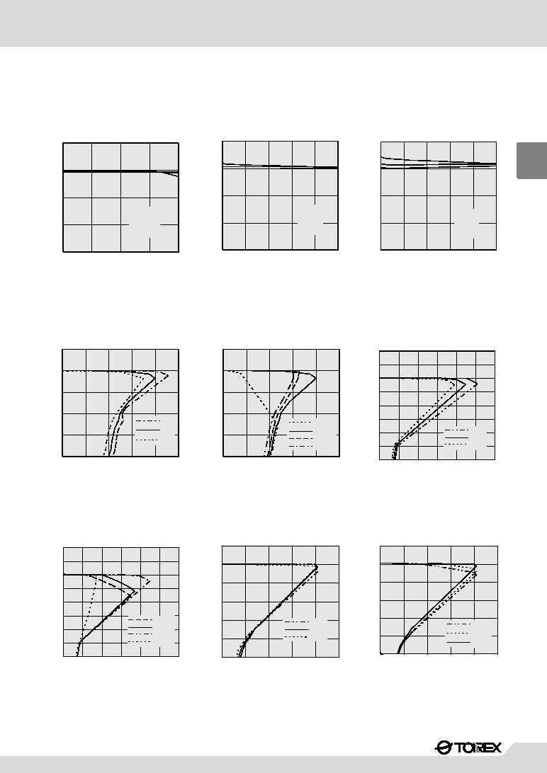
Typical Application Circuit
Typical Performance Characteristic
Preliminary
01S_02XC6206 02.9.19 6:39 PM 17
XC6206
Series
18
1
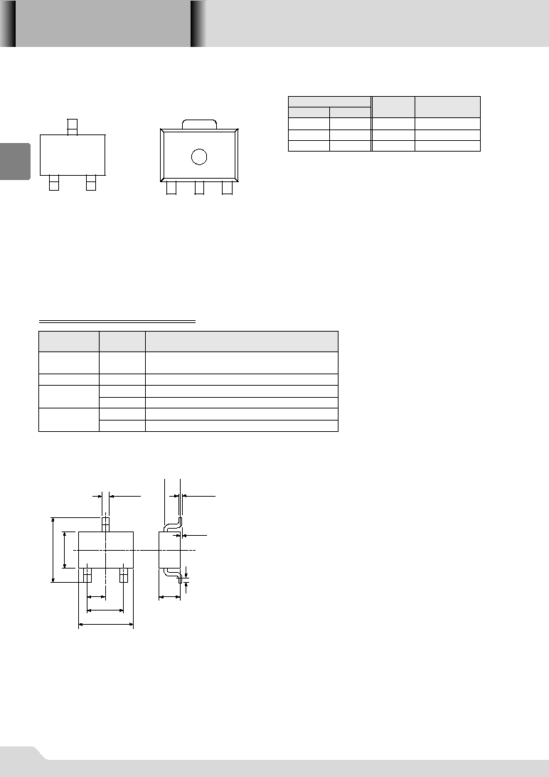
Packaging Information
GSOT-23
Pin Configuration
Pin Assignment
Product Classification
IOrdering Information
V
IN
V
SS
V
OUT
1
2
3
SOT-23
V
SS
V
OUT
V
IN
SOT-89
(TOP VIEW)
PIN NUMBER
SOT-23
SOT-89
PIN
NAME
FUNCTION
1
V
SS
Ground
3
V
IN
Power Input
2
1
2
3
V
OUT
Output
SYMBOL
DESTINATION
DESCRIPTION
qw
Integer
Output Voltage
e.g. q = 3, w = 0
3.0V
e
Accuracy : within
± 2%
2
M
SOT-23
r
P
SOT-89
R
Embossed Tape : Standard Feed
t
L
Embossed Tape : Reverse Feed
XC6206P qwert
1.1±0.1
00.1
0.15
0.95
1.9±0.2
2.9±0.2
0.2min
2.8±0.2
+0.1
-0.05
0.4
+0.1
-0.05
1.6
+0.2
-0.1
01S_02XC6206 02.09.12 11:10 18

XC6206
Series
20
1
Test Circuits
V
IN
V
OUT
V
SS
C
IN
1.0F
(ceramic)
C
L
1.0F
(ceramic)
V
V
A
OPEN
A
V
IN
V
SS
V
OUT
Circuit q
Circuit w
Electrical Characteristics
XC6206P302
(3.0V)
Ta=25
PARAMETER
SYMBOL
CONDITIONS
MIN.
TYP.
MAX.
UNITS
CIRCUIT
Output Voltage
V
OUT
(E)
I
OUT
= 40mA
×0.98
2.940
V
OUT
()
3.000
×1.02
V
3.060
q
Maximum Ouput Current
I
OUTMAX
200
mA
q
Load Regulation
V
OUT
1mA
I
OUT
100mA
25
mV
q
Dropout Voltage
Vdif1
I
OUT
= 30mA
80
mV
Vdif2
I
OUT
= 100mA
250
mV
q
Supply Current
I
DD
V
IN
= 4.0V
1.0
A
w
Line Regulations
V
OUT
V
IN
V
OUT
V
OUT
(T)+1.0V
V
IN
6V
I
OUT
= 40mA
0.01
0.30
%/V
q
Input Voltage
V
IN
1.8
6
V
-
Output Voltage
Temperature Characteristics
V
OUT
T
opr
V
OUT
I
OUT
= 40mA
- 40
T
opr
85
100
ppm
/
q
Current Limiter
Ishort
V
IN
= V
OUT
+1.5VV
OUT
= V
SS
100
mA
q
Note
(NOTE 1) V
OUT
(T) = Specified Output Voltage
(NOTE 2) V
OUT
(E) = Effective Output Voltage (le. The output voltage when "V
OUT
(T)+1.0V" is provided at the V
IN
pin while maintaining
a certain I
OUT
value.)
(NOTE 3) Vdif = {V
IN
1
(NOTE5)
+ V
OUT
1
(NOTE4)
}
(NOTE 4) V
OUT
1 = A voltage equal to 98% of the Output Voltage whenever an amply stabilized I
OUT
{V
OUT
(T) + 1.0V} is input.
(NOTE 5) V
IN
1 = The Input Voltage when V
OUT
1 appears as Input Voltage is gradually decreased.
(NOTE 6) Unless otherwise stated, V
IN
= V
OUT
(T) + 1.0V
01S_02XC6206 02.09.12 11:10 20