1
Data Sheet
ud200527
May 17, 2005 V4
CMOS
Low Power Consumption
Dropout Voltage
: 40mV@30mA
120mV@100mA
Output Voltage Range : 1.2V ~ 5.0V
Output Current
: 300mA <Up to 380mA (TYP.)>
Low ESR Capacitor Compatible
High Ripple Rejection, Low Output Noise
Regulators with Green Operation (GO) Function
CL High-Speed Auto-Discharge (XC6207B)
GENERAL DESCRIPTION
The XC6207 series are precise, low noise, high speed, low
dropout regulators with green operation (GO) function. They
are fabricated using Torex's CMOS process. Performance
features of the series include high ripple rejection and low
dropout voltage, and the series include a reference voltage
source, an error amplifier, a current limiter, and a phase
compensation circuit.
Output voltage is selectable in 50mV increments within a range
of 1.2V~5.0V, using laser trimming technologies.
The series' output stabilization capacitor (CL) is also
compatible with low ESR ceramic capacitors.
GO provides high speed operation, low power consumption
and high efficiencies by automatically switching between a high
speed mode (HS) and a power save mode (PS) depending
upon the load current level. The switching point of the GO to
the output current is being fixed inside the IC. The IC
operates when the GO pin is low-level. When only
high-speed operation is required, it can be fixed by inputting a
high level signal to the GO pin, thus providing operating
conditions with the most suitable level of supply current for the
application.
The CE function enables the output to be turned off resulting in
greatly reduced power consumption. In this state, with the
XC6207B series, the IC turns on the internal switch located
between the VOUT and VSS pins. This short enables the
electric charge at the output capacitor (CL) to be discharged
via the internal auto-discharge resistance, and as a result the
VOUT pin quickly returns to the VSS level.
The constant current limit circuit and the current limiter's
foldback circuit also operate as a short circuit protection for the
output current limiter and the output pin.
APPLICATIONS
Cellular phones
Cordless phones, Wireless communication equipment
Portable games
Cameras, VCRs
Portable AV equipment
PDAs
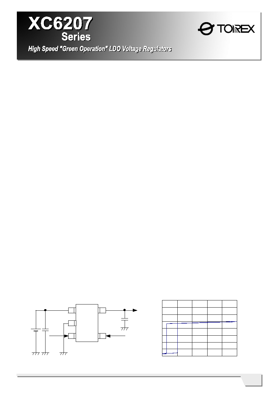
TYPICAL APPLICATION CIRCUIT
FEATURES
Maximum Output Current : 300mA <Up to 380mA (TYP.)>
Dropout Voltage
: 120mV@ I
OUT
=100mA
Operating Voltage Range: 2.0V ~ 6.0V
Output Voltage Setting Range : 1.2V ~ 5.0V (50mV increments)
Accuracy :
±
2% (HS Mode:V
OUT
>1.5V)
2%,-3% (PS Mode:V
OUT
>1.5V)
±
30mV (HS Mode:V
OUT
1.5V)
+30mV, -45mV (PS Mode:V
OUT
1.5V)
Low Power Consumption : 5.5A (TYP.)(PS mode)
50A (TYP.)(HS mode)
Standby Current
: Less than 0.1A
High Ripple Rejection : 70dB @ 1kHz
Operating Temperature Range : -40 ~ 85
Low ESR Capacitor
: Ceramic capacitor compatible
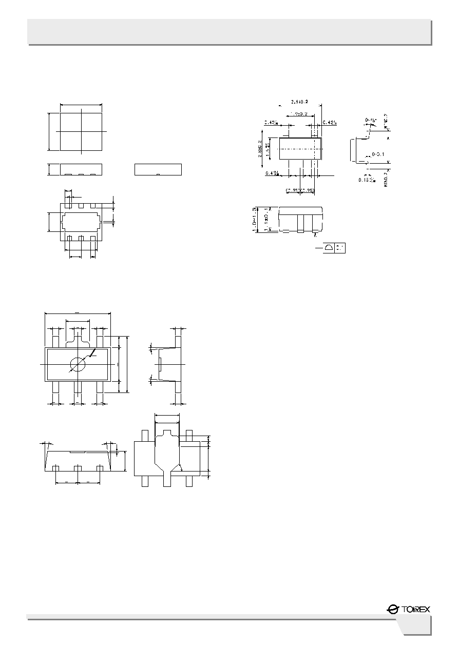
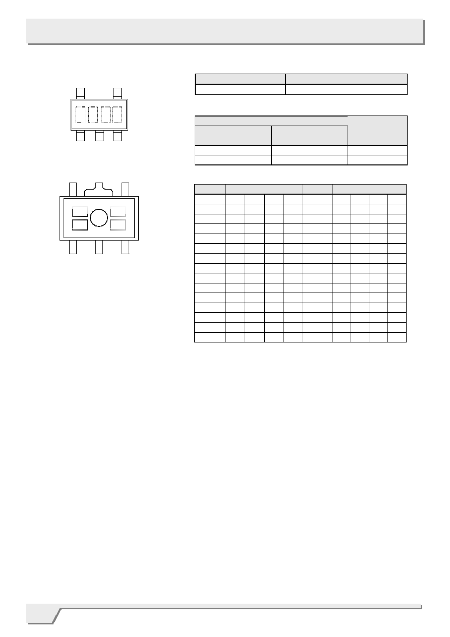
Ultra Small Packages :
SOT-89-5
SOT-25
USP-6C
TYPICAL PERFORMANCE
CHARACTERISTICS
Supply Current vs. Output Current
0
10
20
30
40
50
60
70
80
0
1
2
3
4
5
Output Current IOUT (mA)
Supp
ly
C
u
r
r
e
n
t
I
S
S
(
µ
A)
VIN=CE, VSS=GO=0V
VIN=2.8V, CIN=CL=1.0
µF, Ta=25
O
C
XC6207A182xx
GO-Compatible
V IN
1
2
3
4
5
V SS
V OUT
GO
CE
CIN
1uF
CL
1uF
Input
Input
2
XC6207
Series
Data Sheet
ud200527
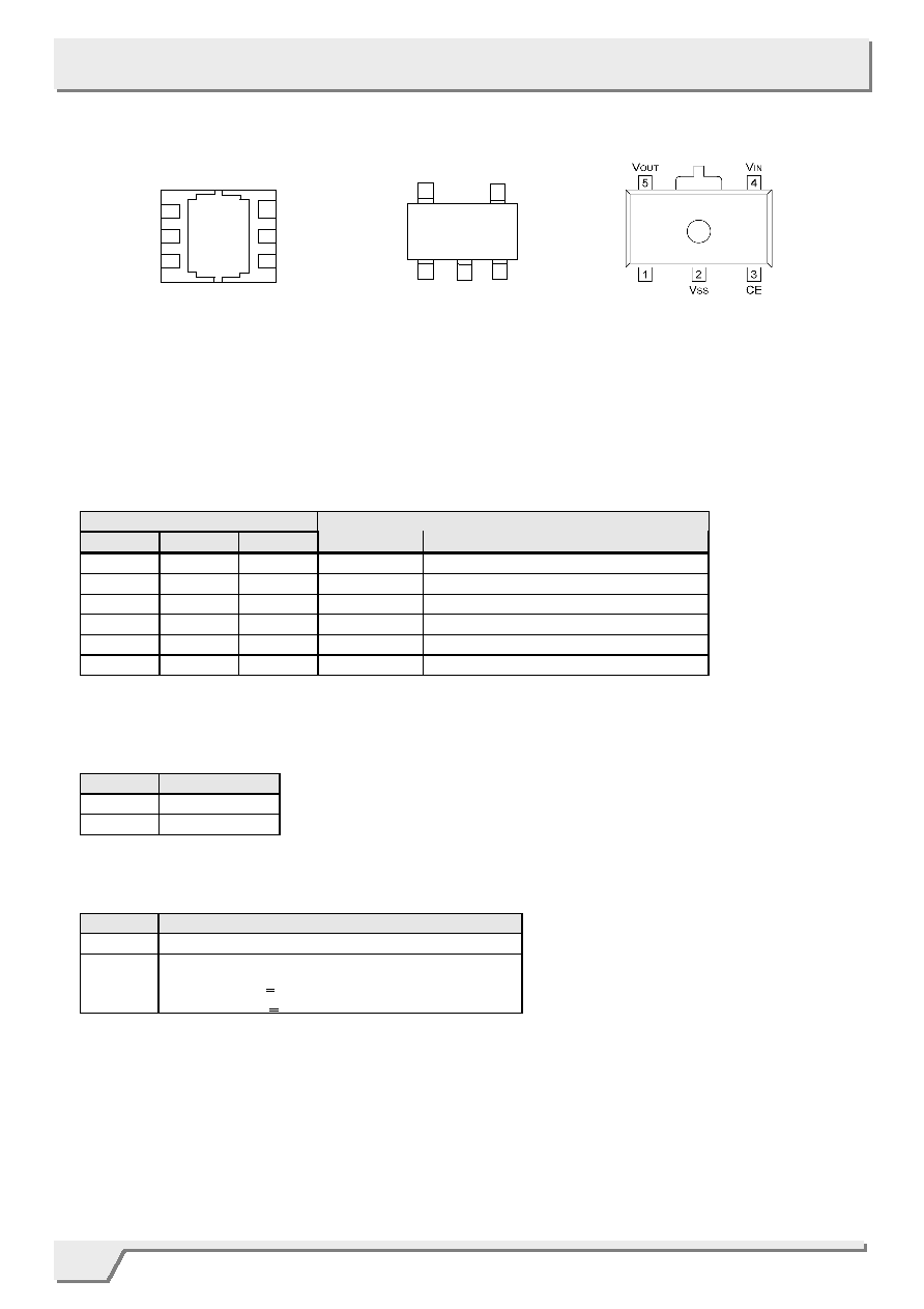
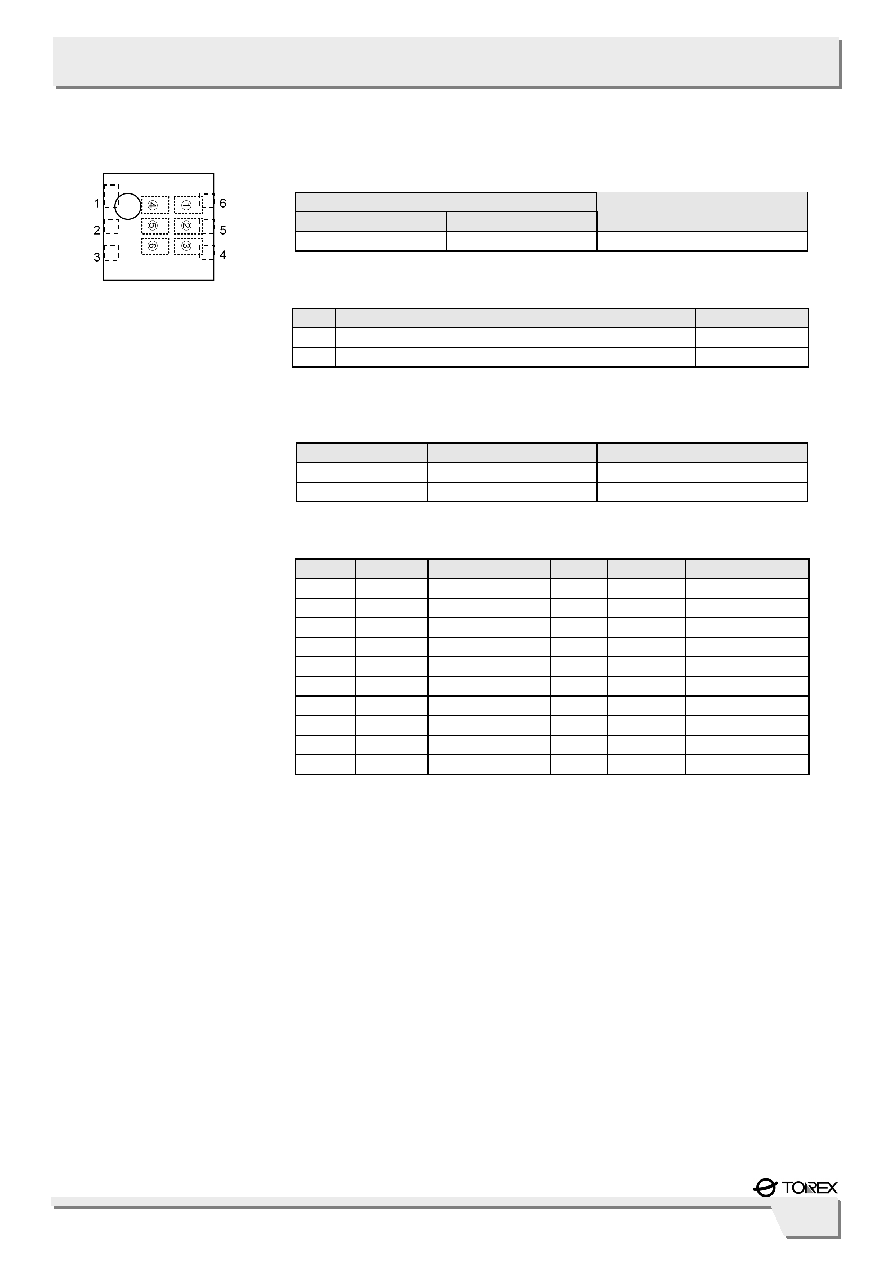
PIN NUMBER
USP-6C
SOT-25
SOT-89-5
PIN NAME
FUNCTIONS
1 1 4 V
IN
Power
Input
2 - - NC
No
Connection
3 5 5 V
OUT
Output
4
4
1
GO
Green Operation Mode Switch
5 2 2 V
SS
Ground
6 3 3 CE
ON/OFF
Control
CE
FUNCTION
H Operation
L Stand
by
GO
FUNCTION
H High
Speed
Mode
L
Green Operation (HS/PS Mode Automatic Switching)
IGO < IOUT High Speed Mode
IGOR > IOUT Power Save Mode
PIN CONFIGURATION
PIN ASSIGNMENT
*The dissipation pad for the USP-6C package should be solder-plated
in recommended mount pattern and metal masking so as to enhance
mounting strength and heat release.
If the pad needs to be connected to other pins, it should be connected
to the VSS pin, No. 5.
SOT-25
(TOP VIEW)
VOUT
VIN
VSS
CE
GO
4
2
5
1
3
FUNCTIONS CHART
GO
SOT-89-5
(TOP VIEW)
CE pin
*For the XC6207B series, the output capacitor (CL) is discharged via the internal auto-discharge resistance when the CE is at low level.
CE pin
VOUT
VSS
CE
VIN
NC
GO
4
5
1
2
3
6
USP-6C
(BOTTOM VIEW)
5
Data Sheet
ud200527
XC6207
Series
MARK
PRODUCT SERIES
0 7 XC6207xxxxxx
MARK
TYPE
PRODUCT SERIES
A
High Active with No Pull-Down Resistor, No CL Discharge Resistor
XC6207AxxxDx
B
High Active with No Pull-Down Resistor, with CL Discharge Resistor
XC6207BxxxDx
MARK
VOLTAGE (V)
PRODUCT SERIES
3 3.X XC6207x3xxDx
5 5.X XC6207x5xxDx
MARK VOLTAGE(V) PRODUCT SERIES
MARK
VOLTAGE(V) PRODUCT SERIES
0 X.0
XC6207xx02/1Dx
A X.05
XC6207xx0A/BDx
1 X.1
XC6207xx12/1Dx
B X.15
XC6207xx1A/BDx
2 X.2
XC6207xx22/1Dx
C X.25
XC6207xx2A/BDx
3 X.3
XC6207xx32/1Dx
D X.35
XC6207xx3A/BDx
4 X.4
XC6207xx42/1Dx
E X.45
XC6207xx4A/BDx
5 X.5
XC6207xx52/1Dx
F X.55
XC6207xx5A/BDx
6 X.6
XC6207xx62/1Dx
H X.65
XC6207xx6A/BDx
7 X.7
XC6207xx72/1Dx
K X.75
XC6207xx7A/BDx
8 X.8
XC6207xx82/1Dx
L X.85
XC6207xx8A/BDx
9 X.9
XC6207xx92/1Dx
M X.95
XC6207xx9A/BDx
Represents product series
Represents type of regulator
Represents production lot number
0 to 9, A to Z repeated (G, I, J, O, Q, W excepted)
Note: No character inversion used.
Represents decimal number of the output voltage
Represents integer of the output voltage
ex)
MARKING RULE (Continued)
USP-6C
(TOP VIEW)