Äîêóìåíòàöèÿ è îïèñàíèÿ www.docs.chipfind.ru
XC6209 Series
High Speed LDO Regulators, Low ESR Cap. Compatible, Output On/Off Control
February 1
7, 2004 V5
!
Low Power Consumption
: 25
µ
A (TYP.)
!
APPLICATIONS
!
Dropout Voltage
: 30mA @ 60mV
"
Mobile phones, Cordless phones
: 100mA @ 200mV
"
Wireless communication equipment
!
Output Current
: 150mA (XC6209A ~D series)
"
Portable games
: 300mA (XC6209E ~H series)
"
Cameras, Video recorders
!
Highly Accurate
: ± 2% (± 30mV less than 1.5V)
"
Portable AV equipment
!
Output Voltage Range
: 0.9V ~ 6.0V (50mV Step)
"
Reference voltage
!
Low ESR capacitor compatible
"
Battery powered equipment
!
GENERAL DESCRIPTION
!
FEATURES
Maximum Output Current (*)
: 150mA (XC6209A ~ D series)
: 300mA (XC6209E ~ H series)
Dropout Voltage
: 200mV @ IOUT=100mA
Operating Voltage Range
: 2.0V ~ 10V
Output Voltage Range
: 0.9V ~ 6.0V (50mV Step)
Highly Accurate
: ± 2% (VOUT>1.5V)
: ± 30mV (VOUT<1.5V)
Low Power Consumption
: 25
µ
A (TYP.)
Standby Current
: Less than 0.1
µ
A (TYP.)
High Ripple Rejection
: 70dB (10kHz)
Operating Temperature Range
: - 40
O
C ~ + 85
O
C
Low ESR Capacitor Compatible
: Ceramic capacitor
Ultra Small Packages
: SOT-25
SOT-89-5
USP-6B
* Maximum output current of the XC6209E ~ H series
depends on the setting voltage.
!
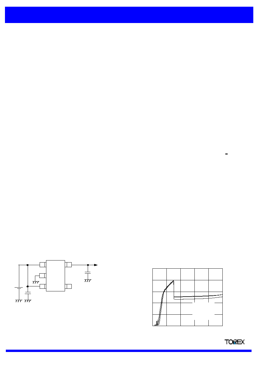
TYPICAL APPLICATION CIRCUIT
!
TYPICAL PERFORMANCE CHARACTERISTICS
#
Supply Current vs. Input Voltage
The XC6209 series are precise, low noise, positive voltage LDO
regulators manufactured using CMOS processes. The series
achieves high ripple rejection and low dropout and consists of a
voltage reference, an error amplifier, a current limiter and a phase
compensation circuit plus a driver transistor.
Output voltage is selectable in 50mV increments within a range of
0.9V ~ 6.0V.
The series is also compatible with low ESR ceramic capacitors
which give added output stability. This stability can be maintained
even during load fluctuations due to the excellent transient
response of the series.
The current limiter's foldback circuit also operates as a short
protect for the output current limiter and the output pin.
The CE function enables the output to be turned off, resulting in
greatly reduced power consumption.
V
IN
V
OUT
NC
CE
CL
1
µ
F
V
SS
CIN
1
µ
F
54
3
2
1
Semiconductor Ltd.
XC6209x302
0
10
20
30
40
50
0
2
4
6
8
10
Input Voltage VIN (V)
S
uppl
y
C
ur
r
e
nt
I
S
S
(
µ
A)
Topr= 85
O
C
= 25
O
C
= - 40
O
C
Data Sheet
1

XC6209 Series
High Speed LDO Regulators, Low ESR Cap. Compatible, Output On/Off Control
!
PIN CONFIGURATION
!
PIN ASSIGNMENT
!
SELECTION GUIDE
The following options for the CE pin logic and internal pull-up/down are available:
High Active + no pull-down resistor built-in (standard)
High Active + 2.0M
pull-down resistor built-in <between CE-VSS> (semi-custom)
Low Active + no pull-up resistor built-in (semi-custom)
Low Active + 2.0M
pull-up resistor built-in <between VIN-CE> (semi-custom)
Note: *With the pull-up resistor or pull-down resistor built-in types, the supply current during operation will increase by VIN / 2.0M
(TYP.).
!
ORDERING INFORMATION
XC6209
123456
Output Voltage : 100mV Step
Accuracy : within
±
2% (*Note2)
e.g.
2
=2,
3
=8,
4
=2
2.80V
Output Voltage : 50mV Step
Accuracy : within
±
2% (*Note 2)
e.g.
2
=2,
3
=8,
4
=A
2.85V
Package Type :
SOT-25
SOT-89
USP - 6B
Output Voltage :
Device Orientation :
e.g. 3.0V =
2
: 3,
3
: 0
Embossed Tape : Standard Feed
Embossed Tape : Reverse Feed
(Note 1) Maximum output current of the XC6209E ~ H series depend on the setting voltage.
(Note 2) Within ± 30mV (VOUT<1.5V)
Output
Ground
ON/OFF Control
No Connection
DESCRIPTION
FUNCTION
Input
CE
NC
VOUT
3
3
6
VSS
1
(*Note1)
SOT-25
SOT-89-5
USP-6B
2
2
5
1
1
2
4
1
2, 4
5
5
3
M
PIN NAME
4
D / H
SYMBOL
4
5
DESCRIPTION
Active 'Low'
(no pull-up resistor built in, stanard)
VIN
Integer
PIN NUMBER
6
D
R
L
DESIGNATOR SYMBOL
DESIGNATOR
A / E
B / F
C / G
P
High Active
(pull-down resistor built in, semi-custom)
High Active
(no pull-down resistor built in, standard)
Low Active
(pull-up resistor built in, semi-custom)
A
2 3
4
2
5
1
3
CE
(NC)
VIN VSS
VOUT
SOT-25 (TOP VIEW)
USP-6B (BOTTOM VIEW)
VOUT
5
VSS
2
VIN
4
1
NC
2
VSS
3
CE
SOT-89 (TOP VIEW)
Semiconductor Ltd.
*Please do not connect a heat dissipation pad to
the circuitry. If the pad needs to be connected to
the circuitry, it should be connected to the VSS
pin.
3 VOUT
2 NC
1 VIN
NC 4
VSS 5
CE 6
Data Sheet
2
XC6209 Series
High Speed LDO Regulators, Low ESR Cap. Compatible, Output On/Off Control
!
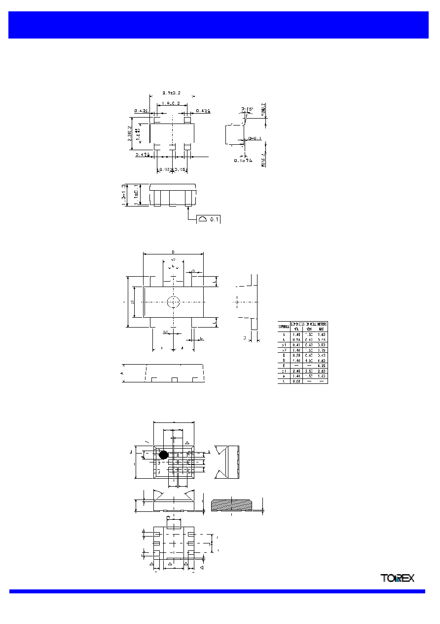
PACKAGING INFORMATION
#
SOT-25
#
SOT-89-5
#
USP-6B
6
5
4
1
2
3
A'
A
AA
A
A
A
A
1
.
4
5
6
3
2
1
0
1
1
1
1
1
2.0 + 0.15
(0.45) 0.5+0.1
(0.05)
(0.45) (0.45)
45
O
45
O
1
.
8+
0.
1
5
(0
.
2
7
)
(0.2
7)
(0.2
7)
( 0
.
45
)
45
O
45
O
(0.12
5
)
(0
.
6
5
)
0.00
5+0.00
2
(0
.
0
5
)
-0
.
005
+0
.
0
1
-0.05
+0
.
1
5
0.7+0.03
5-0.2
+
0
.
05
0.
5+0.1
1
.
6+0.1
5
0.
5+0.1
0
.
1+
0.
0
3
0.2+0
.
05
1.0+0.1
0.25+0.1
0.25+0.1
O
Semiconductor Ltd.
* Pin no. 1 is thicker than other pins.
Data Sheet
3
XC6209 Series
High Speed LDO Regulators, Low ESR Cap. Compatible, Output On/Off Control
!
MARKING RULE
#
SOT-25 & SOT-89-5
1
Represents product series
* Sequential number for custom products (0 to 9 or A to Z)
2
Represents the type of voltage regulator
3
Represents output voltage
4
Represents production lot number
0 to 9, A to Z, reversed character of 0 to 9 and A to Z repeated (G,I,J,O,Q excepted)
3.05
-
3.00
6.00
2.85
5.85
2.90
5.90
2.95
5.95
2.80
5.80
2.65
5.65
2.70
5.70
2.75
5.75
2.60
5.60
2.45
5.45
2.50
5.50
2.55
5.55
2.40
5.40
2.25
5.25
2.30
5.30
2.35
5.35
2.20
5.20
2.05
5.05
2.10
5.10
2.15
5.15
2.00
5.00
1.85
4.85
1.90
4.90
1.95
4.95
1.80
4.80
1.65
4.65
1.70
4.70
1.75
4.75
1.60
4.60
E
Z
1.50
4.50
1.55
4.55
D
Y
1.40
4.40
1.45
4.45
C
X
1.30
4.30
1.35
4.35
B
V
1.20
4.20
1.25
4.25
A
U
1.10
4.10
1.15
4.15
9
T
1.00
4.00
1.05
4.05
8
S
0.90
3.90
0.95
3.95
7
R
-
3.80
-
3.85
6
P
-
3.70
-
3.75
5
N
-
3.60
-
3.65
4
M
-
3.50
-
3.55
3
L
-
3.40
-
3.45
2
K
-
3.30
-
3.35
1
H
-
3.20
-
3.25
0
F
-
3.10
-
3.15
XC6209Exxxxx
XC6209Fxxxxx
XC6209Gxxxxx
XC6209Hxxxxx
XC6209Axxxxx
XC6209Bxxxxx
XC6209Cxxxxx
XC6209Dxxxxx
N
D
K
P
C
H
L
B
F
M
A
E
N
D
K
P
C
H
L
B
F
M
A
E
V
X
Y
Z
PRODUCT SERIES
SYMBOL
PRODUCT SERIES
9
XC6209xxxxxx
SYMBOL
SYMBOL
OUTPUT VOLTAGE (V)
VOUT 100mV STEPS
VOUT 50mV STEPS
VOUT=
0.1~3.0V
VOUT=
3.1~6.0V
VOUT=
0.15~3.05V
VOUT=
3.15~6.05V
SYMBOL
OUTPUT VOLTAGE (V)
V
X
Y
Z
1234
1
2
3
4
SOT-25
(TOP VIEW)
SOT-89-5
(TOP VIEW)
Semiconductor Ltd.
Data Sheet
4
XC6209 Series
High Speed LDO Regulators, Low ESR Cap. Compatible, Output On/Off Control
!
MARKING RULE (Continued)
#
USP-6B
1 2
Represents product series
3
Represents the type of voltage regulator
4
Represents the integer of output voltage
5
Represents the decimal point of output voltage
4
Represents production lot number
0 to 9, A to Z, reversed character of 0 to 9 and A to Z repeated (G,I,J,O,Q excepted)
CE Pin, High Active with no pull-down resistor
CE Pin, High Active with pull-up resistor
CE Pin, High Active with no pull-up resistor
X.95
XC6209xx9ADx
X.75
XC6209xx7ADx
XC6209xx5ADx
X.85
XC6209xx8ADx
X.45
XC6209xx4ADx
X.55
X.65
XC6209xx6ADx
X.25
XC6209xx2ADx
X.35
XC6209xx3ADx
X.05
XC6209xx0ADx
X.15
XC6209xx1ADx
XC6209xx4xDx
XC6209xx5xDx
F
E
XC6209xx6xDx
XC6209xx7xDx
7
K
6
H
X.6
X.7
9
M
8
L
X.8
X.9
XC6209xx8xDx
XC6209xx9xDx
3
D
XC6209xx3xDx
5
X.3
X.4
X.5
4
2
C
1
B
X.1
X.2
XC6209xx1xDx
XC6209xx2xDx
5
XC6209x5xxDx
5.X
A
0
X.0
SYMBOL
OUTPUT VOLTAGE (V)
SYMBOL
XC6209xx0xDx
3
3.X
PRODUCT SERIES
XC6209x3xxDx
SYMBOL
TYPE
D
XC6209DxxxDx
C
SYMBOL
XC6209AxxxDx
B
XC6209BxxxDx
A
TYPE
CE Pin, High Active with pull-down resistor
PRODUCT SERIES
SYMBOL
XC6209AxxxDx
PRODUCT SERIES
2
1
0
9
XC6209CxxxDx
OUTPUT VOLTAGE (V)
USP-6B
(TOP VIEW)
Semiconductor Ltd.
6
5
4
1
2
3
1
23
4
56
Data Sheet
5
Document Outline