XC6212 Series
High Speed LDO Regulators, Low ESR Cap. Compatible, Output ON/OFF Control
October 27, 2003 V3
!
Low Power Consumption
: 25
µ
A (TYP.)
!
APPLICATIONS
!
Dropout Voltage
: 60mV @ 30mA
"
Mobile phones, Cordless phones
: 200mV @ 100mA
"
Wireless communication equipment
!
Maximum Output Current
: up to 150mA
"
Portable games
!
Highly Accurate
:
±
2% (
±
30mV less than 1.5V)
"
Cameras, Video recorders
!
Output Voltage Range
: 0.9V ~ 6.0V (50mV Step)
"
Portable AV equipment
!
Low ESR capacitor compatible
"
Reference voltage
"
Battery powered equipment
!
GENERAL DESCRIPTION
!
FEATURES
Maximum Output Current
: 150mA
Dropout Voltage
: 200mV (IOUT=100mA)
Maximum Operating Voltage
: 2.0V ~ 10V
Output Voltage Range
: 0.9V~6.0V (50mV Step)
Highly Accurate
: ±2% (VOUT>1.5V)
: ±30mV (VOUT
1.5V)
Low Power Consumption
: 25mA (TYP.)
Standby Current
: Less than 0.1mA (TYP.)
High Ripple Rejection
: 70dB (10kHz)
Operating Temperature Range
: -40
O
C ~ +85
O
C
Low ESR Capacitor Compatible
: Ceramic capacitor
Ultra Small Packages
: SOT-25 (SOT-23-5)
!
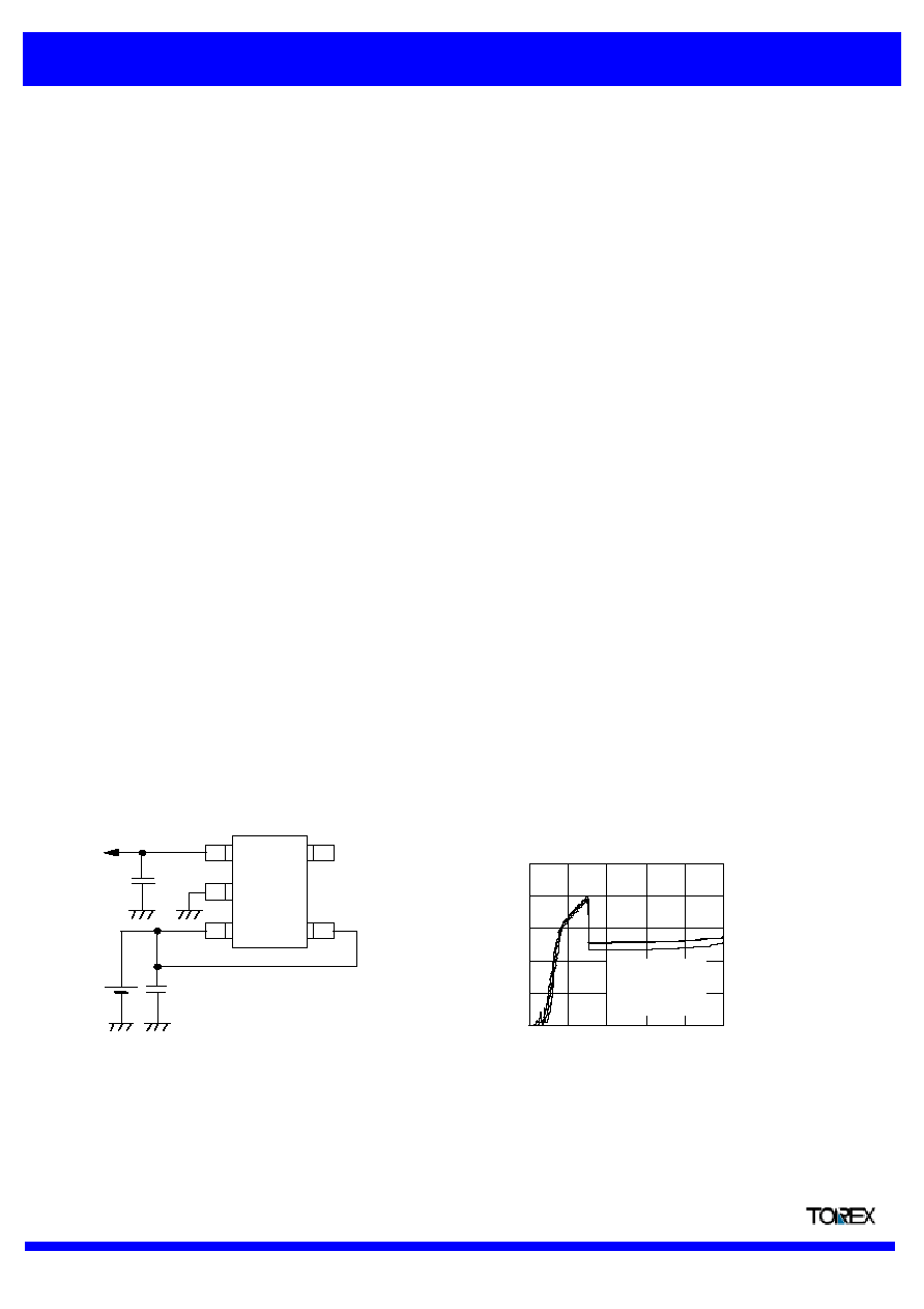
TYPICAL APPLICATION CIRCUIT
!
TYPICAL PERFORMANCE CHARACTERISTICS
The XC6212 series are highly precise, low noise, positive voltage LDO
regulators manufactured using CMOS processes. The series achieves
high ripple rejection and low dropout and consists of a voltage reference,
an error amplifier, a current limiter and a phase compensation circuit
plus a driver transistor.
Output voltage is selectable in 50mV increments within a range of 0.9V ~
6.0V.
The series is also compatible with low ESR ceramic capacitors which
give added output stability. This stability can be maintained even during
load fluctuations due to the excellent transient response of the series.
The current limiter's foldback circuit also operates as a short protect for
the output current limiter and the output pin.
The CE function enables the output to be turned off, resulting in greatly
reduced power consumption.
C
I N
1
µ
F
CL
1
µ
F
V
OUT
V
SS
V
IN
CE
NC
5
4
3
2
1
0
10
20
30
40
50
0
2
4
6
8
10
Input Voltage V
IN
(V)
Supply Current I
SS
(
µ
A)
XC6212 x 302
Topr = 85
O
C
= 25
O
C
= - 40
O
C
Semiconductor Ltd.
1

XC6212 Series
High Speed LDO Regulators, Low ESR Cap. Compatible, Output ON/OFF Control
!
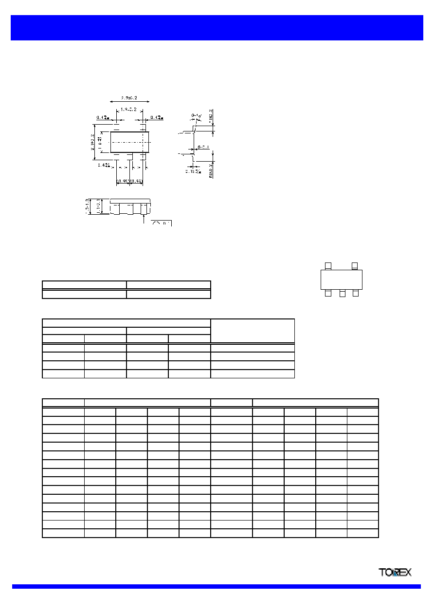
PIN CONFIGURATION
!
PIN ASSIGNMENT
!
BLOCK DIAGRAM
!
SELECTION GUIDE
The following options for the CE pin logic and internal pull-up/down are available:
Active 'High' + no pull-down resistor built-in (standard)
Active 'High' + 2.0M
pull-down resistor built-in <between CE-VSS> (semi-custom)
Active 'Low' + no pull-up resistor built-in (semi-custom)
Active 'Low' + 2.0M
pull-up resistor built-in <between VIN-CE> (semi-custom)
Note: *With the pull-up resistor or pull-down resistor built-in types, the supply current during operation will increase by VIN / 2.0M
(TYP.).
!
ORDERING INFORMATION
XC6212
123456
Output Voltage : 100mV Step
Accuracy : within
±
2%
e.g.
2
=2,
3
=8,
4
=2
2.80V
Output Voltage : 50mV Step
Accuracy : within
±
2%
e.g.
2
=2,
3
=8,
4
=A
2.85V
Output Voltage :
Device Orientation :
e.g. 3.0V =
2
: 3,
3
: 0
Embossed Tape : Standard Feed
Embossed Tape : Reverse Feed
PIN NUMBER
No Connection
NC
1
Integer
2 3
6
R
L
1
A
B
C
D
5
DESCRIPTION
Active 'Low', No pull-up resistor built in
(Semi-custom)
DESIGNATOR
Active 'High', Pull-down resistor built in
(Semi-custom)
Active 'High',
No pull-down resistor built in (Standard)
Active 'Low', Pull-up resistor built in
(Semi-custom)
VSS
Output
Ground
DESIGNATOR SYMBOL
Power Input
ON / OFF Control
3
4
2
VOUT
PIN NAME
FUNCTION
SOT-25
4
5
M
VIN
CE
SOT-25 (SOT-23-5)
Package Type :
DESCRIPTION
SYMBOL
A
2
4
2
5
1
3
CE
NC
V
IN
V
SS
V
OUT
SOT-25 (SOT-23-5)
(TOP VIEW)
V
SS
V
OUT
V
IN
Current
Limiter
ON/OFF
Control
Voltage
Reference
each circuit
CE
R2
R1
Semiconductor Ltd.
2
XC6212 Series
High Speed LDO Regulators, Low ESR Cap. Compatible, Output ON/OFF Control
!
PACKAGING INFORMATION
#
SOT-25 (SOT-23-5)
!
MARKING RULE
#
SOT-25 (SOT-23-5)
1
Represents product series
2
Represents the type of voltage regulator
3
Represents output voltage
4
Represents production lot number
0 to 9, A to Z, reversed character of 0 to 9 and A to Z repeated (G,I,J,O,Q excepted)
3.05
-
2.95
5.95
E
1.50
4.50
1.55
4.55
Z
3.00
6.00
2.85
5.85
D
1.40
4.40
1.45
4.45
Y
2.90
5.90
2.75
5.75
C
1.30
4.30
1.35
4.35
X
2.80
5.80
2.65
5.65
B
1.20
4.20
1.25
4.25
V
2.70
5.70
2.55
5.55
A
1.10
4.10
1.15
4.15
U
2.60
5.60
2.45
5.45
9
1.00
4.00
1.05
4.05
T
2.50
5.50
2.35
5.35
8
0.90
3.90
0.95
3.95
S
2.40
5.40
2.25
5.25
7
-
3.80
-
3.85
R
2.30
5.30
2.15
5.15
6
-
3.70
-
3.75
P
2.20
5.20
2.05
5.05
5
-
3.60
-
3.65
N
2.10
5.10
1.95
4.95
4
-
3.50
-
3.55
M
2.00
5.00
1.85
4.85
3
-
3.40
-
3.45
L
1.90
4.90
1.75
4.75
2
-
3.30
-
3.35
K
1.80
4.80
1.65
4.65
1
-
3.20
-
3.25
H
1.70
4.70
3.15
F
1.60
4.60
0
-
3.10
-
XC6212CxxxMx
Z
D
K
P
XC6212DxxxMx
XC6212AxxxMx
X
B
F
M
XC6212BxxxMx
V
A
E
L
SYMBOL
PRODUCT SERIES
9
XC6212xxxxMx
SYMBOL
PRODUCT SERIES
VOUT 100mV STEPS
VOUT 50mV STEPS
OUTPUT VOLTAGE (V)
SYMBOL
OUTPUT VOLTAGE (V)
SYMBOL
Y
C
H
N
VOUT=0.1~3.0V VOUT=3.1~6.0V
VOUT=0.15~3.05V
VOUT=3.15~6.05V
1234
SOT-25 (SOT-23-5)
(TOP VIEW)
Semiconductor Ltd.
3
XC6212 Series
High Speed LDO Regulators, Low ESR Cap. Compatible, Output ON/OFF Control
!
ABSOLUTE MAXIMUM RATINGS
!
ELECTRICAL CHARACTERISTICS
XC6212B SERIES
Ta=25
O
C
(NOTE 1) VOUT(T)=Specified Output Voltage
(NOTE 2) VOUT(E)=Effective Output Voltage
(I.e. the output voltage when "VOUT(T)+1.0V" is provided at the VIN pin while maintaining a certain IOUT value).
(NOTE 3) Vdif={VIN1
(NOTE5)
-VOUT1
(NOTE4)
}
(NOTE 4) VOUT1=A voltage equal to 98% of the Output Voltage whenever an amply stabilized IOUT {VOUT(T)+1.0V} is input.
(NOTE 5) VIN1=The Input Voltage when VOUT1 appears as Input Voltage is gradually decreased.
(NOTE 6) Unless otherwise stated, VIN=VOUT(T)+1.0V
VCE=VIN
VCE=VSS
VCE=VSS
VOUT(T)+1.0V
VIN
10V
IOUT=30mA
1mA
IOUT
100mA
IOUT=30mA
IOUT=100mA
VCE=VIN
CONDITIONS
IOUT=30mA
UNITS
PARAMETER
Input Voltage
RATINGS
SYMBOL
V
IOUT
mA
VIN
V
VOUT
12
500
VSS -0.3 ~ VIN +0.3
O
C
Tstg
VCE
TYP.
Topr
UNITS
2
-
ppm/
O
C
1
mA
1
mV
15
50
mV
mV
V
µ
A
100
IOUT=30mA
% / V
10
-40
O
C
Topr
85
O
C
IOUT=50mA, f=10kHz
Line Regulation
VIN
VOUT
VOUT /
Ripple Rejection Rate
PSRR
1
70
50
-0.10
2
4
mA
300
1
dB
µ
A
0.10
µ
A
2
0.10
VIN
mA
1
V
0.25
V
1
2
0.01
CE "Low" Voltage
VCEL
Temperature Characteristics
VOUT /
Topr
VOUT
Output Voltage
Ilim
Input Voltage
150
Maximum Output Current
IOUTMAX
CIRCUIT
1
MIN
MAX
V
◊
1.02
1
25
50
µ
A
2
0.01
0.10
PARAMETER
SYMBOL
Output Voltage
VOUT (E)
1
2
CE "High" Voltage
VCEH
1.60
Short-circuit Current
Ishort
VIN
CE "High" Current
ICEH
-0.10
CE "Low" Current
ICEL
E-1 (page 5)
E-2 (page 5)
0.20
IDD
Dropout Voltage
Standby Current
Istby
Current Limiter
Vdif1
VOUT(T)
mW
V
VSS -0.3 ~ VIN +0.3
250
Pd
-55 ~ +125
Vdif2
Load Regulation
VOUT
Supply Current
-40 ~ +85
◊
0.98
O
C
Operating Ambient Temperature
Storage Temperature
Output Current
Output Voltage
Power Dissipation
SOT-23-5
CE Input Voltage
Semiconductor Ltd.
4

XC6212 Series
High Speed LDO Regulators, Low ESR Cap. Compatible, Output ON/OFF Control
!
DROPOUT VOLTAGE
* The input voltage 2.0V (Min.) is needed to operate the series. When the output voltage is less than 2.0V,
2.0V-VOUT(T) of dropout voltage is needed at minimum.
230
180
270
200
250
-
50
70
-
60
80
70
100
120
0.9
1.5
1150
-
60
90
-
60
90
200
-
-
70
100
-
80
120
-
200
210
220
270
240
330
220
290
240
310
400
280
380
350
80
120
240
510
550
600
80
500
2.1 ~ 2.2
-
1.8
1.9
TYP
MAX
500
1110
300
1200
TYP
MAX
E-2
Vdif 2
160
210
1100
1100
SYMBOL
5.0 ~ 6.0
2.3 ~ 2.4
2.5 ~ 2.7
2.8 ~ 2.9
3.0
4.0 ~ 4.9
3.1 ~ 3.9
E-1
100
2.0
120
150
Vdif 1
200
MIN
-
-
MIN
1100
500
200
100
-
-
-
-
-
-
-
PARAMETER
OUTPUT VOLTAGE
Semiconductor Ltd.
5