1
XC6214 ETR0318_004.doc
FEATURES
Maximum Output Current : More than 500mA
(800mA limit)
Dropout Voltage
: 500mV @ I
OUT
= 500mA
(V
OUT
=3.3V)
Operating Voltage Range : 1.8V ~ 6.0V
Output Voltage
: 1.5V, 1.8V, 2.5V, 3.3V, (standard)
3.0V (under development)
Other voltages between 1.5V to
5.0V (semi-custom)
High Accuracy
: Setting voltage accuracy ±2%
Low Power Consumption
Ripple Rejection Rate
: 8A (TYP.)
: 40dB @ 1kHz
Operating Temperature
Range
: - 40 ~ 85
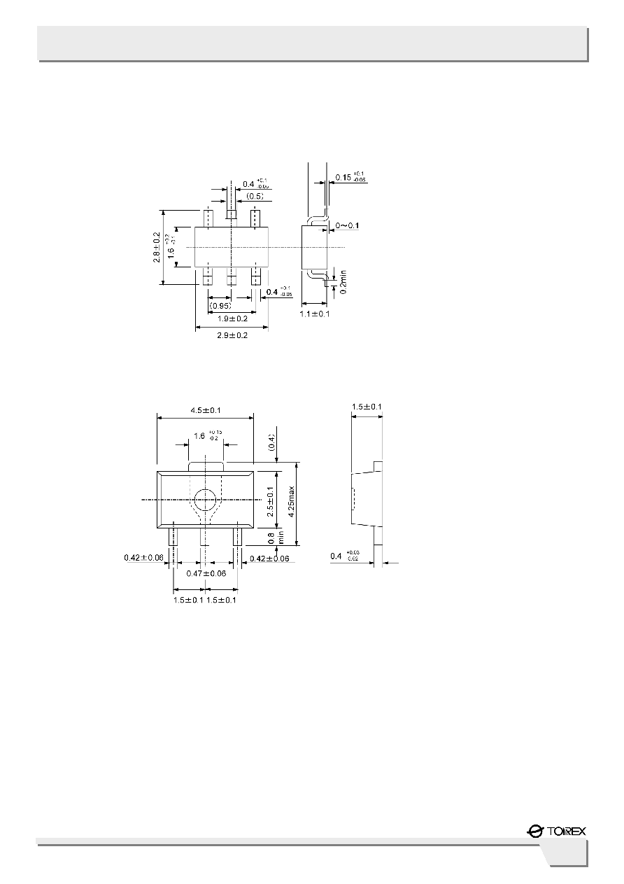
Packages
: SOT-26
SOT-89
CMOS Low Power Consumption : 8A (TYP.)
Maximum Output Current : More than 500mA
Current Limit Circuit Built-In
Thermal Shutdown Circuit Built-In
Ceramic Capacitor Compatible
GENERAL DESCRIPTION
The XC6214 series are highly precise, low noise, high current,
positive voltage low dropout regulators. They are fabricated
using Torex's CMOS process. The series features a voltage
reference, an error amplifier, a current limiter, a thermal
protection circuit, and a phase compensation circuit plus a
driver transistor.
The output voltage is selectable in 100mV increments within the
range of 1.5V to 5.0V
.
(Output voltage 1.5V, 1.8V, 2.5V, and
3.3V are standard products. Output voltage 3.0V is under
development to be a standard product. Other than these
voltages are available as semi-custom products.)
The series is also compatible with low ESR ceramic capacitors,
which give added output stability. This stability can be
maintained even during load fluctuations due to the excellent
transient response of the series.
The over current protection circuit and the thermal shutdown
circuit are built in. The over current protection circuit will
operate when the output current reaches current limit level.
The thermal shutdown circuit will operate when the junction
temperature reaches temperature limit level.
APPLICATIONS
DVD, CD-ROM, HDD drive equipment
Portable AV equipment (Cameras, VCRs, etc.)
Wireless Communication equipment
(Mobile & Cordless phone, etc.)
Desktop computers, Note book computer, PDAs
Network equipment (Wireless LAN etc.)
Reference voltage
Battery powered equipment
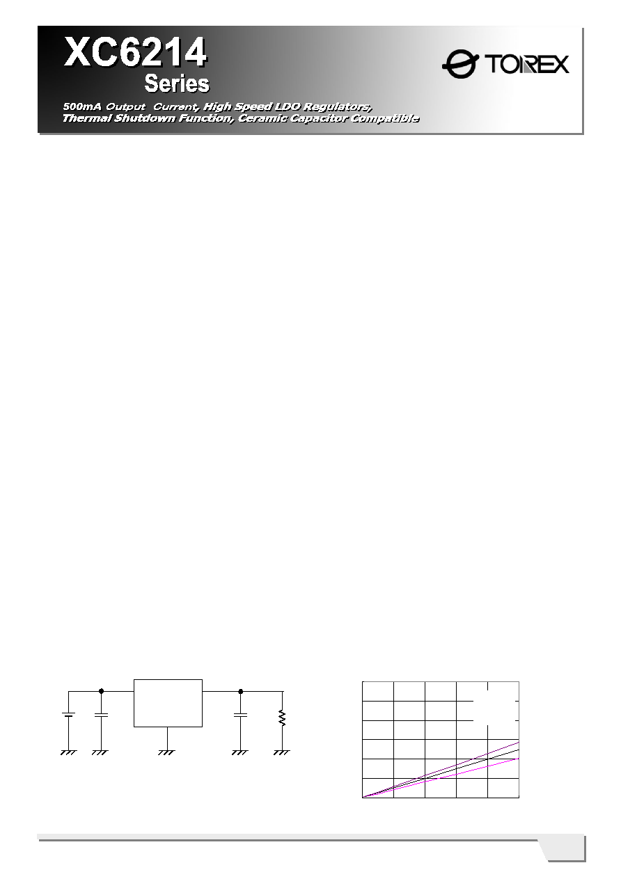
TYPICAL APPLICATION CIRCUIT
TYPICAL PERFORMANCE
CHARACTERISTICS
Dropout Voltage vs. Output Current
XC6214P332
0.0
0.2
0.4
0.6
0.8
1.0
1.2
0
100
200
300
400
500
Output Current : IOUT (mA)
D
r
opout
V
o
l
t
a
ge :
V
d
i
f
(
V
)
CIN=CL=1.0µF(ceramic)
Topr=85
o
C
25
o
C
-40
o
C
V
OUT
V
SS
V
IN
C
IN
1.0uF
C
L
1.0uF
R
L
V
IN
2
XC6214
Series
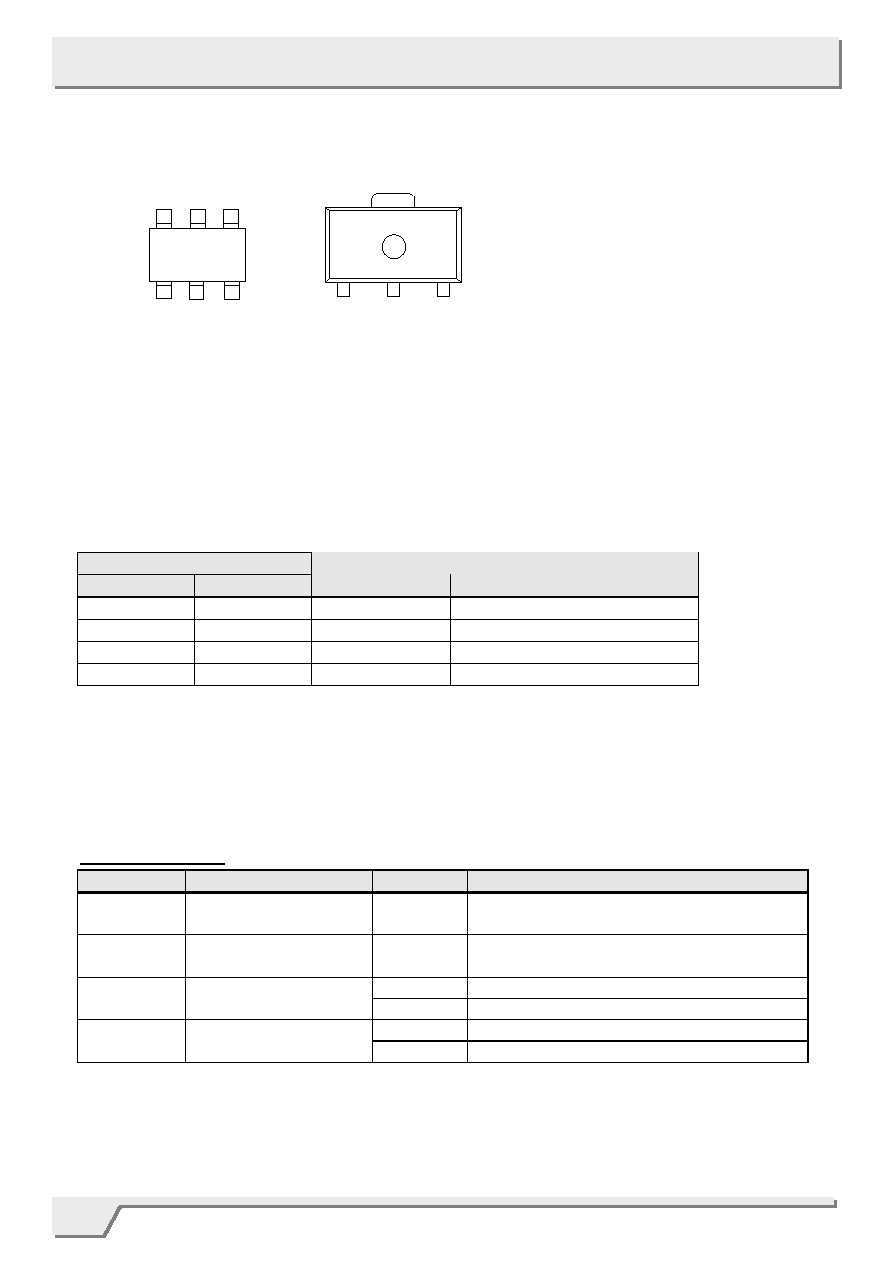
PIN NUMBER
SOT-26
SOT-89
PIN NAME
FUNCTIONS
1 2 V
IN
Power
Input
2, 4, 5
1
V
SS
Ground
3 - NC
No
Connection
6 3 V
OUT
Output
DESIGNATOR
DESCRIPTION
SYMBOL
DESCRIPTION
Output Voltage
15 ~ 50
: ex.) 3.0V products =3, =0
Output Voltage Accuracy
2
: Within ±2%
ex.) 2.50V products =2, =5, =2
M :
SOT-26
Package
P :
SOT-89
R
: Embossed tape, standard feed
Device Orientation
L
: Embossed tape, reverse feed
PIN CONFIGURATION
* The 2, 4 and 5 pins of the SOT-26 package
are the common V
SS
pins in the package.
For a heat design, in case of connecting the
heat dissipation pad to a circuit,
Please use the 2, 4, and 5 pins as the V
SS
pin on the PCB board
PIN ASSIGNMENT
PRODUCT CLASSIFICATION
XC6214P
Ordering Information
SOT-26 (TOP VIEW)
SOT-89 (TOP VIEW)
2
3
1
1
2
3
4
5
6
4
XC6214
Series
MARK
PRODUCT SERIES
D XC6214Pxx2xx
MARK
VOLTAGE (V)
PRODUCT SERIES
P
1.5 ~ 3.0
XC6214Pxx2xx
R
3.1 ~ 5.0
XC6214Pxx2xx
MARK
VOLTAGE (V)
MARK
VOLTAGE (V)
0 -
3.1
F
1.6
4.6
1 -
3.2
H
1.7
4.7
2 -
3.3
K
1.8
4.8
3 -
3.4
L 1.9
4.9
4 -
3.5
M
2.0
5.0
5 -
3.6
N
2.1
-
6 -
3.7
P
2.2
-
7 -
3.8
R
2.3
-
8 -
3.9
S
2.4
-
9 -
4.0
T
2.5
-
A -
4.1
U
2.6
-
B -
4.2
V 2.7
-
C -
4.3
W
2.8
-
D -
4.4
Y 2.9
-
E 1.5
4.5 Z 3.0
-
MARK
PRODUCTION YEAR
4 2004
5 2005
MARK
MONTH
MARK
MONTH
MARK
MONTH
A January E May J
September
B February F June K October
C March G July L
November
D April H August
M
December
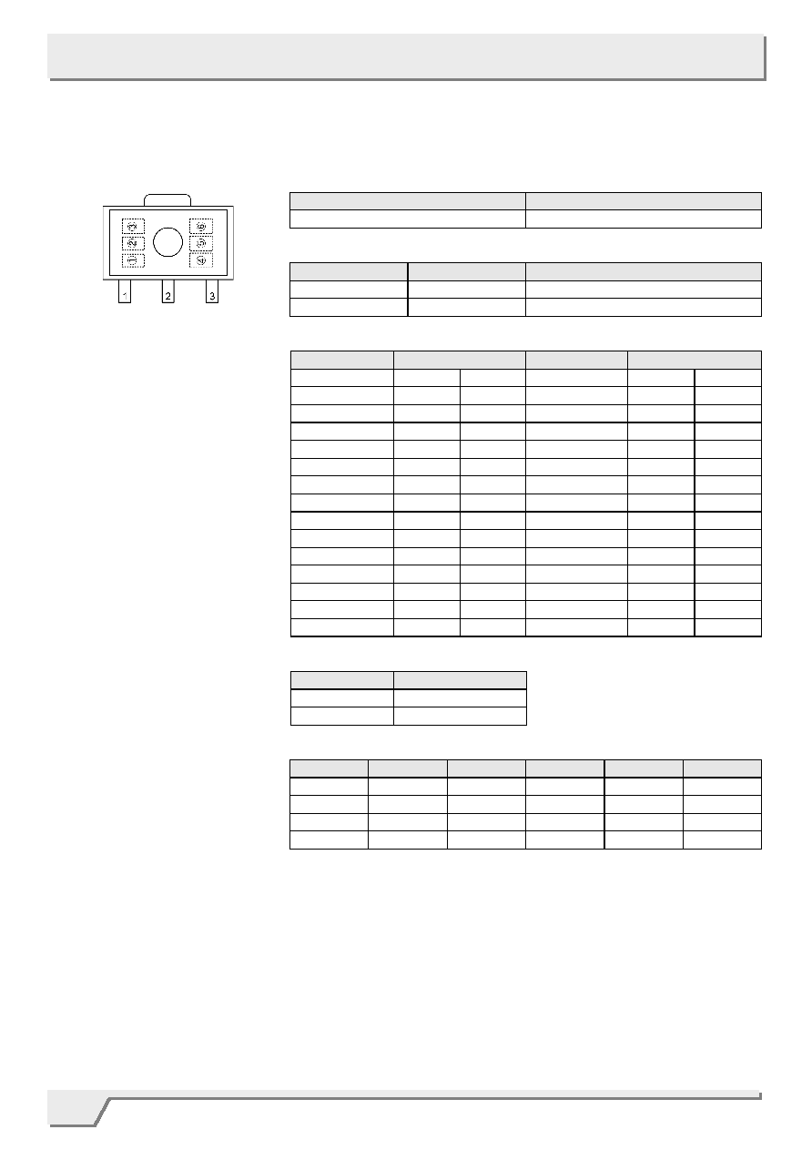
MARKING RULE
SOT-89
Represents product series
Represents output voltage range
Represents output voltage
Represents the last digit of the production year (ex.)
Represents the production month
Represents production lot number
0 to 9, A to Z repeated (G, I, J, O, Q, W excepted).
Note: No character inversion used.
SOT89
(TOP VIEW)
5
XC6214
Series
MARK
PRODUCT SERIES
D XC6214Pxx2xx
MARK
VOLTAGE (V)
PRODUCT SERIES
P
1.5 ~ 3.0
XC6214Pxx2xx
R
3.1 ~ 5.0
XC6214Pxx2xx
MARK
VOLTAGE (V)
MARK
VOLTAGE (V)
0 -
3.1
F
1.6
4.6
1 -
3.2
H
1.7
4.7
2 -
3.3
K
1.8
4.8
3 -
3.4
L 1.9
4.9
4 -
3.5
M
2.0
5.0
5 -
3.6
N
2.1
-
6 -
3.7
P
2.2
-
7 -
3.8
R
2.3
-
8 -
3.9
S
2.4
-
9 -
4.0
T
2.5
-
A -
4.1
U
2.6
-
B -
4.2
V 2.7
-
C -
4.3
W
2.8
-
D -
4.4
Y 2.9
-
E 1.5
4.5 Z 3.0
-
MARK
a
b
c
d
PRODUCTION YEAR
- -
- 2004
- - -
2005
- - -
2006
-
- -
2007
MARK
MARK
e
f
g
h
PRODUCTION
MONTH
e
f
g
h
PRODUCTION
MONTH
- - -
January
- July
-
- -
February
-
-
-
August
- -
March
-
-
September
- -
- April -
-
October
-
- May
-
November
-
- June -
-
December
MARKING RULE (Continued)
SOT-26
Represents product series
Represents output voltage range
Represents output voltage
a, b, c, d Represents production year
Represents production lot number
0 to 9, A to Z repeated (G, I, J, O, Q, W excepted).
Note: No character inversion used.
SOT-26
(TOP VIEW)
e, f, g, h Represents production month
*Markings of the year 2004 to 2007 are repeated from 2008.
ex.) 20042008, 20052009, 20062010, 20072011.
1
2
3
4
6
5
a
b
c
d
e
f
g
h