Data Sheet
1
R000026
XC6219 Series
High Speed LDO Regulators, Low ESR Cap. Compatible, ON/OFF Switch
October 4, 2004 V5
CMOS Low Power Consumption
APPLICATIONS
Dropout Voltage
60mV @ 30mA
Mobile phones
200mV
@
100mA
Cordless phones and radio communication equipment
Output Current
150mA (VOUT<1.75V)
Portable games
240mA (VOUT>1.8V)
Cameras, video cameras
(300mA limit)
Reference voltage sources
Highly Accurate
+ 2%
Battery powered equipment
(+30mV when VOUT>1.5V)
Output Voltage Range
0.9V to 5.0V (50mV increments)
Low ESR Ceramic Capacitor Compatible
GENERAL
DESCRIPTION
FEATURES
The XC6219 series are highly accurate, low noise, CMOS LDO
Maximum Output Current
150mA (VOUT<1.75V)
Voltage Regulators. Offering low output noise, high ripple rejection
240mA (VOUT>1.8V)
ratio, low dropout and very fast turn-on times, the XC6219 series
(300mA limit (TYP))
is ideal for today's cutting edge mobile phone.
Dropout Voltage
200mV (IOUT=100mA)
Internally the XC6219 includes a reference voltage source, error
Operating Voltage Range
2.0V ~ 6.0V
amplifiers, driver transistors, current limiters and phase
Output Voltage Range
0.9V ~ 5.0V (50mV steps)
compensators. The XC6219's current limiters' foldback circuit
Highly Accurate
+ 2% (VOUT>1.5V)
also operates as a short protect for the output current limiter and.
+30mV (VOUT<1.5V)
the output pin. The output voltage is set by laser trimming.
Low Power Consumption
25
�A (TYP.)
Voltages are selectable in 50mV steps within a range of
Standby Current
Less than 0.1
�A (TYP.)
0.9V to 5.0V. The XC6219 series is also fully compatible with low
High Ripple Rejection
65dB (10kHz)
ESR ceramic capacitors, reducing cost and improving output stability.
Operating Temperature Range
- 40
O
C to 85
O
C
This high level of output stability is maintained even during frequent
Low ESR Ceramic Compatible
Ceramic Capacitor
load fluctuations, due to the excellent transient response performance
Ultra Small Packages
SOT-25 (SOT-23-5)
and high PSRR achieved across a broad range of frequencies.
SOT-89
The CE function allows the output of regulator to be turned off,
USP-6B
resulting in greatly reduced power consumption.
The XC6219 series is available in the SOT-25 (SOT-23-5), SOT-89
or USP-6B `chip-scale' package. Measuring only 2.0mm x 1.8mm
the USP-6B is perfect for applications where PCB area is critical.
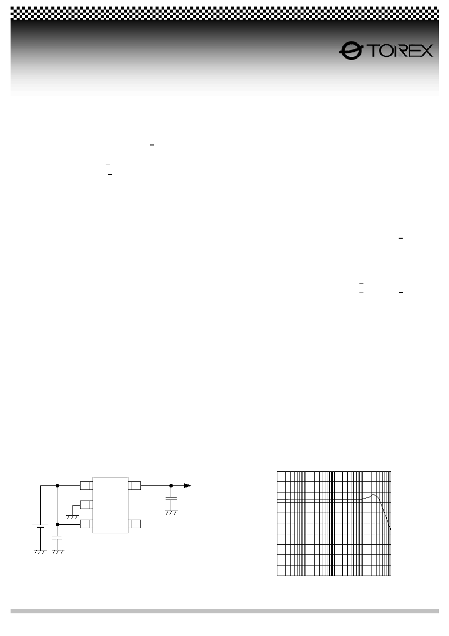
TYPICAL
APPLICATION
CIRCUIT
TYPICAL PERFORMANCE CHARACTERISTICS
Ripple Rejection Rate
SOT-25 (SOT-23-5)
VSS
1
2
3
4
5
VIN
VOUT
CE
NC
CIN
1�F
CL
1�F
0
10
20
30
40
50
60
70
80
90
100
0.01
0.1
1
10
100
Ripple Frequency f (kHz)
Ri
p
p
l
e
Re
j
e
c
t
i
o
n
Ra
t
e
RR (d
B
)
XC6219x302
VIN=3.0V, DC+1Vp-pAC
IOUT=50mA, CL=1uF (ceramics)
Data Sheet
2
R000026
XC6219 Series
High Speed LDO Regulators, Low ESR Cap. Compatible, ON/OFF Switch
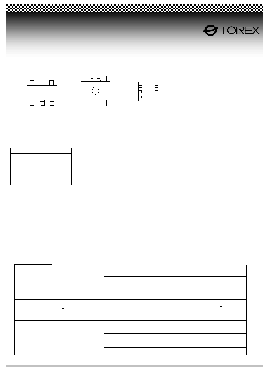
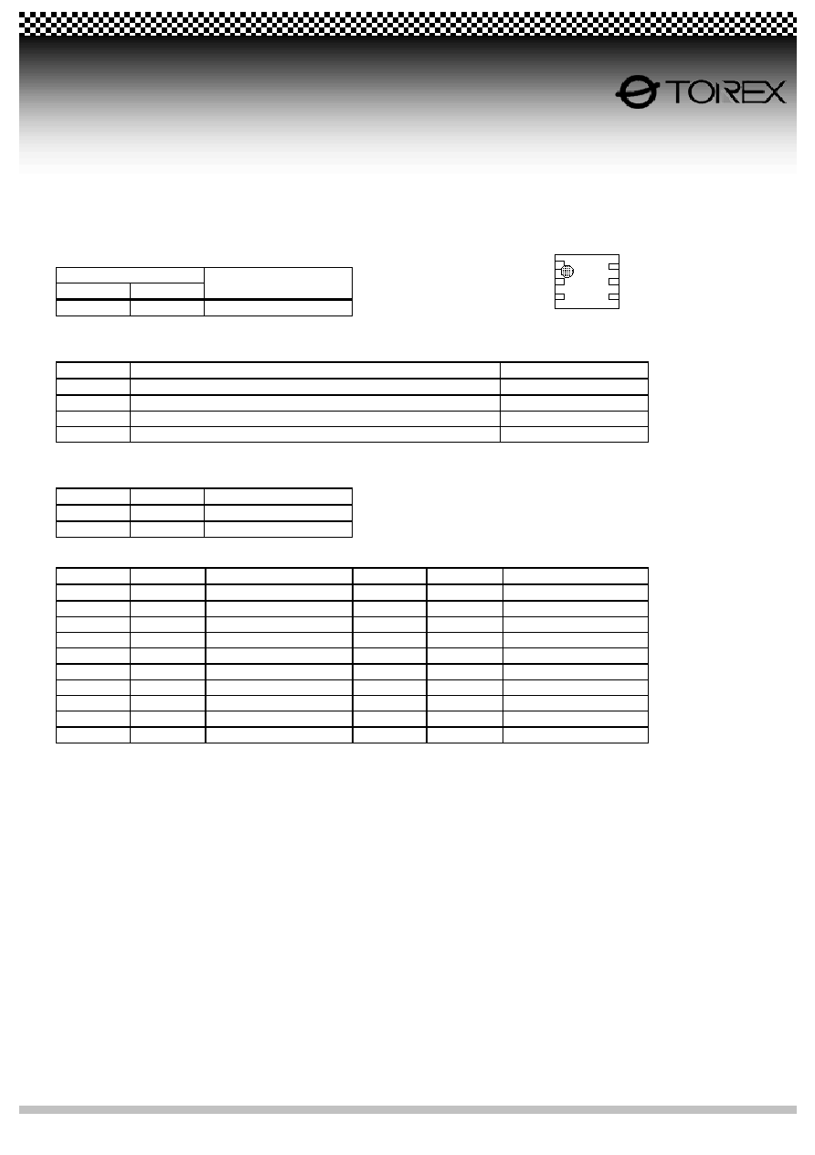
PIN CONFIGURATION
*Please use the circuit without connecting to the heat dissipation pad.
If the pad needs to be connected to other pins, it should be
noted that the pin configuration of the USP-6B package is
different depending on the IC series.
SOT-25 (SOT-23-5)
SOT-89-5
USP-6B
(TOP VIEW)
(TOP VIEW)
(BOTTOM VIEW)
PIN ASSIGNMENT
PIN NUMBER
SOT-25 SOT-89-5 USP-6B
PIN NAME
FUNCTIONS
1 4 1 VIN
Power
Input
2 2 5 VSS
Ground
3 3 6 CE ON
/
OFF
Control
4
1
2, 4
NC
No Connection
5 5 3 VOUT
Output
PRODUCT CLASSIFICATION
Selection Guide
The following options for the CE pin logic and internal pull-up/down are available:
High Active + no pull-down resistor built-in (standard)
High Active + 2.0M
pull-down resistor built-in <between CE-VSS> (semi-custom)
Low Active + no pull-up resistor built-in (semi-custom)
Low Active + 2.0M
pull-up resistor built-in <between VIN-CE> (semi-custom)
Note: *With the pull-up resistor or pull-down resistor built-in types, the supply current during operation will increase by VIN / 2.0M
(TYP.)
Ordering Information
XC6219
123456
DESIGNATOR DESCRIPTION
SYMBOL
DESCRIPTION
A
: High Active (ull-down resistor built in)
B
: High Active (no pull-down resistor built in)
C
: Low Active (pull-up resistor built in)
1
CE Pin Logic
D
: Low Active (no pull-up resistor built in)
2 3
Output Voltage
09 ~ 50
: e.g.
2
=3,
3
=0, 3.0V
Output Voltage, 100mV increments,
+2% accuracy
2
: e.g.
2
=2,
3
=8,
4
=2 2.80V, +2%
4
Output Voltage, 50mV increments,
+2% accuracy
A
: e.g.
2
=2,
3
=8,
4
=A 2.85V, +2%
M
: SOT-25 (SOT-23-5)
P :
SOT-89-5
5
Packages
D :
USP-6B
R
: Embossed tape, Standard feed
6
Taping Direction
L
: Embossed tape, Reverse feed
VOUT
5
VSS
2
VIN
4
1
NC
2
VSS
3
CE
6
5
4
1
2
3
VIN
NC
VOUT
CE
VSS
NC
4
2
5
1
3
CE
(NC)
V
IN
V
SS
V
OUT
Data Sheet
3
R000026
XC6219 Series
High Speed LDO Regulators, Low ESR Cap. Compatible, ON/OFF Switch
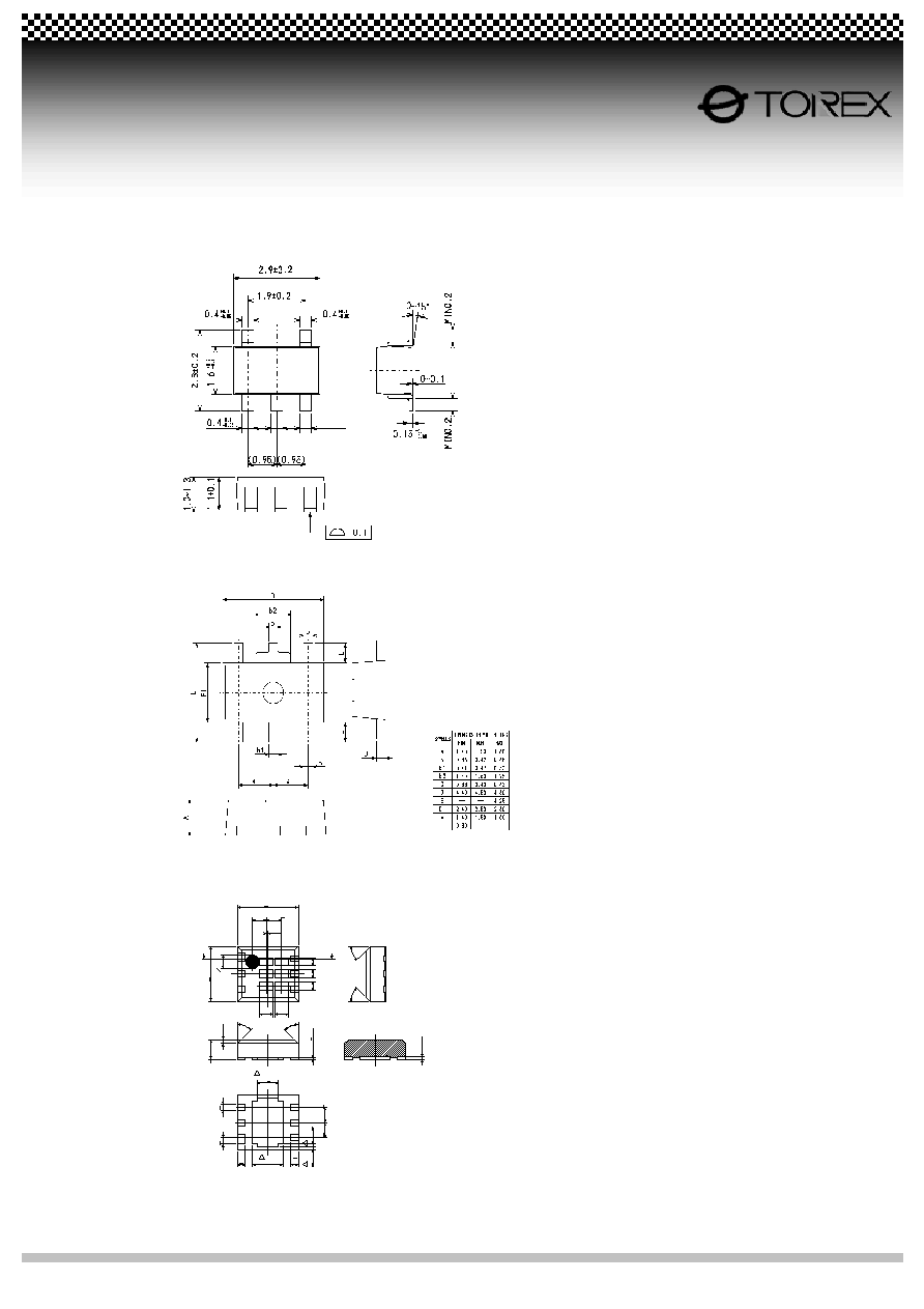
PACKAGING INFORMATION
SOT-25 (SOT-23-5)
SOT-89-5
USP-6B
* Pin no. 1 is thicker than other pins
45
45
6
5
4
1
2
3
A'
A
AA
A
A
A
4
5
6
3
2
1
2
45
45
2
2
2
O
O
A - A' cross-section
drawing
2.0 + 0.15
0.5+0.1
(0.45)
(0.05)
(0
.
2
7
)
(0
.
2
7
)
(0
.
2
7
)
(
0.45)
1.8 +
0.1
5
(0.45) (0.45)
O
0.005
+
0
.00
2
O
O
(
0
.1
25)
0.
6
5
+0.1
5
-0
.
0
5
0.
05
+0
.01
-
0
.005
0.2
+
0.
05
0.7 + 0.03
0.2
+
0.0
5
0.25+0.1 1.0+0.1
0.25+0.1
0
.
5+
0.1
0.
5
+
0.
1
0.
1+
0
.
03
0
.
1+
0
.
03
Data Sheet
4
R000026
XC6219 Series
High Speed LDO Regulators, Low ESR Cap. Compatible, ON/OFF Switch
MARKING RULE
SOT-25 (SOT-23-5)
1
Represents product series
MARK PRODUCT
SERIES
L XC6219xxxxMx
SOT-25 (TOP VIEW)
2
Represents type of regulator
MARK
VOUT 100mV STEPS
VOUT 50mV STEPS
VOUT:0.1~3.0V VOUT:3.1~6.0V
VOUT:0.15~3.05V
VOUT:3.15~6.05V
PRODUCT SERIES
V A E L
XC6219AxxxMx
X B F M
XC6219BxxxMx
Y C H N
XC6219CxxxMx
Z D K P
XC6219DxxxMx
3
Represents output voltage
MARK
OUTPUT VOLTAGE
MARK
OUTPUT VOLTAGE
0 -
3.1
-
3.15
F
1.6
4.6
1.65
4.65
1 -
3.2
-
3.25
H
1.7
4.7
1.75
4.75
2 -
3.3
-
3.35
K
1.8
4.8
1.85
4.85
3 -
3.4
-
3.45
L
1.9
4.9
1.95
4.95
4 -
3.5
-
3.55
M
2.0
5.0
2.05
5
- 3.6 - 3.65
N
2.1 2.15
6
- 3.7 - 3.75
P
2.2 2.25
7
- 3.8 - 3.85
R
2.3 2.35
8 0.9
3.9
0.95
3.95 S 2.4
2.45
9 1.0
4.0
1.05
4.05 T 2.5
2.55
A 1.1
4.1
1.15
4.15 U 2.6
2.65
B 1.2
4.2
1.25
4.25 V 2.7
2.75
C 1.3
4.3
1.35
4.35 X 2.8
2.85
D 1.4
4.4
1.45
4.45 Y 2.9
2.95
E 1.5
4.5
1.55
4.55 Z 3.0
3.05
4
Represents production lot number
0 to 9, A to Z, reverse character of 0 to 9, A to Z repeated. (G, I, J, O, Q, W excepted)
1234
Data Sheet
5
R000026
XC6219 Series
High Speed LDO Regulators, Low ESR Cap. Compatible, ON/OFF Switch
MARKING RULE (Continued)
USP-6B
1
2
Represents product series
MARK
1
2
PRODUCT SERIES
L XC6219xxxxDx
USP-6B (TOP VIEW)
3
Represents type of regulator
MAKR TYPE PRODUCT
SERIES
A
High Active, Pull-down resistor built-in (semi-custom)
XC6219AxxxMx
B
High Active, Pull-down resistor built-in (semi-custom)
XC6219BxxxMx
C
Low Active, Pull-up resistor built-in (semi-custom)
XC6219CxxxMx
D
Low Active, Pull-up resistor built-in (semi-custom)
XC6219DxxxMx
4
Represents product series
MARK VOLTAGE PRODUCT
SERIES
3 3.X XC6219x3xxDx
5 5.X XC6219x5xxDx
3
Represents output voltage
MARK
VOLTAGE
PRODUCT SERIES
MARK
VOLTAGE
PRODUCT SERIES
0 X.0 XC6219xx0xDx A X.05 XC6219xx0ADx
1 X.1 XC6219xx1xDx B X.15 XC6219xx1ADx
2 X.2 XC6219xx2xDx C X.25 XC6219xx2ADx
3 X.3 XC6219xx3xDx D X.35 XC6219xx3ADx
4 X.4 XC6219xx4xDx E X.45 XC6219xx4ADx
5 X.5 XC6219xx5xDx F X.55 XC6219xx5ADx
6 X.6 XC6219xx6xDx H X.65 XC6219xx6ADx
7 X.7 XC6219xx7xDx K X.75 XC6219xx7ADx
8 X.8 XC6219xx8xDx L X.85 XC6219xx8ADx
9 X.9 XC6219xx9xDx M X.95 XC6219xx9ADx
4
Represents production lot number
0 to 9, A to Z repeated. (G, I, J, O, Q, W excepted)
* No character inversion used.
6
5
4
1
2
3
1
23
4
56