Boosting Voltage Regulators
Series
347
3
General Description
Features
Applications
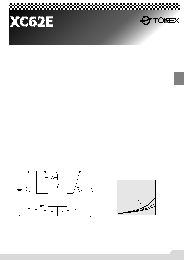
Typical Application Circuit
The XC62E series are a group of positive output voltage regulators that
can supply up to 1A of output current using an external transistor. Low
power and high accuracy are achieved through CMOS process and laser
trimming technologies.
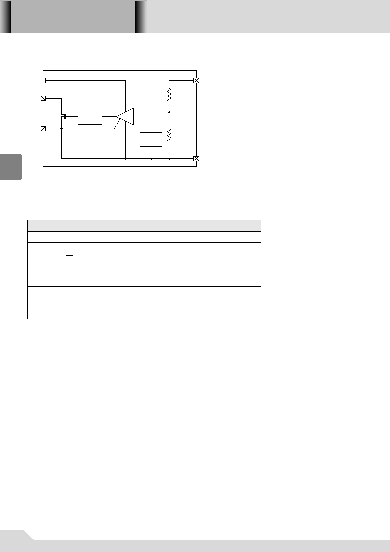
The series consists of a high precision voltage reference, an error
correction circuit and a short-circuit protected output driver.
In stand-by mode, supply current can be dramatically cut. Since the
input-output voltage differential is small, loss control efficiency is good.
The XC62E is particularly suited for use with battery operated portable
products, and products where supply current regulation is required.
The series comes in an ultra small SOT-25 package.
In connection with the CE function, apart from the negative logic
XC62EP series, a positive logic XC62ER series (custom) is also
available.
Ultra Small Input-Output Voltage Differential
: 100mA of output current is
available with a differential of 0.1V.
(Performance depends on the
external transistor characteristics.)
Maximum Output Current : 1000mA
Output Voltage Range :
1.5V ~ 6V in 0.1V increments
Highly Accurate
: Set-up voltage ±2%
Low Power Consumption : Typ.50
µA (V
OUT
=5.0V)
: Typ.0.2
µA (Stand-by)
Output Voltage Temperature Characteristics
: Typ.±100ppm/°C
Input Stability
: Typ.0.1%/V
Ultra Small Packages
: SOT-25 mini-mold
GPortable Cameras and Video Recorders
GBattery Powered Equipment
GPalmtops
GReference Voltage Sources
NCMOS Low Power Consumption
NSmall Input-Output Voltage Differential
: 0.1V @ 100mA
NMaximum Output Current : 1000mA
NOutput Voltage Range : 1.5V~6V
NOutput Voltage Accuracy : ±2%
P
V
IN
V
OUT
Vss
CE
R
BE
R
B
EXT
R
V
IN
PNP Tr
C
IN
Tantalum
C
L
Tantalum
0.0
0.4
0.6
0.8
1.0
0
200
1000
Input/Output Diff.:Vdif
V
Output Current:I
OUT
mA
XC62EP33023.3V
C
L
10
µFtantalum
0.2
400
600
800
Topr25
80
-30
Typical Performance
Characteristic
03S_09XC62E 02.9.12 3:07 PM 347
XC62E
Series
351
3
Electrical Characteristics
XC62EP3002
V
OUT
(T)=3.0V
(Note1)
1. V
OUT
(T)=Specified Output Voltage .
2. V
OUT
(E)=Effective Output Voltage (i.e. the output voltage when "V
OUT
(T)+1.0V" is provided at the V
IN
pin while maintaining a certain I
OUT
value).
3. Vdif= {V
IN
1
(Note5)
-V
OUT
1
(Note4)
}
4. V
OUT
1= A voltage equal to 98% of the Output Voltage whenever an amply stabilised I
OUT
{V
OUT
(T)+1.0V} is input.
5. V
IN
1= The Input Voltage when V
OUT
1 appears as Input Voltage is gradually decreased.
6. The characteristics for those parameters marked with an asterisk* are liable to vary depending on which transistor is used.
Please use a transistor with a low saturation voltage level and h
FE
equal to 100 or more.
7. The maximum output current value is not a value representing continuous output due to the limitations of the 2AS1213 transistor's power
dissipation.
Note:
PARAMETER
CONDITIONS
MIN
TYP
MAX
UNITS
SYMBOL
Output Voltage
I
OUT
=50mA
V
IN
=4.0V
2.940
1000
3.000
3.060
V
Load Stability*
V
IN
=4.0V
mA
I
OUT
max.
Maximum Output Current*
Input-OutputVoltage
Differential
(Note3)
V
IN
=4.0V
1mA
I
OUT
100mA
0.2
60
-60
mV
V
OUT
Supply Current1
I
OUT
=100mA
I
OUT
=50mA
4.0V
V
IN
8.0V
I
OUT
=10mA
30
°C Topr 80°C
100
mV
Vdif
Supply Current2
Input Stability*
EXT Output Voltage
EXT Leak Current
CE "High" Level Current
CE "Low" Level Current
Input Voltage
Output Voltage
Temperature Characteristics*
V
IN
=4.0V, V
CE
=V
SS
V
IN
=8.0V,V
CE
=V
IN
50
0.1
±100
0.05
0.6
0.3
8
0.5
0.1
0
µA
80
µA
%/V
V
ppm/
°C
V
8
µA
µA
µA
I
SS
1
I
SS
2
V
IN
V
EXT
I
LEAK
1.5
CE "High" Level Voltage
CE "Low" Level Voltage
0.25
V
V
V
CEH
V
CEL
I
CEH
I
CEL
V
CE
=V
IN
V
CE
=V
SS
V
OUT
V
IN ·
V
OUT
V
OUT
T
opr ·
V
OUT
Ta=25
°C
V
OUT
(E)
(Note2)
The characteristics for the XC62ER series are the same as above except for the CE operating logic which is the opposite.
03S_09XC62E 02.9.12 3:07 PM 351