Positive Voltage Regulators
Series
285
3
The XC62FP series is a group of positive voltage output, three-pin
regulators, that provide a high current even when the input/output
voltage differential is small. Low power consumption and high accuracy
is achieved through CMOS and laser trimming technologies.
The XC62FP consists of a high-precision voltage reference, an error
amplification circuit, and a current limited output driver. Transient
response to load variations have improved in comparison to the existing
series.
SOT-23 (150mW), SOT-89 (500mW) and TO-92 (300mW) packages are
available.
Maximum Output Current
: 250mA
(within max. power dissipation, V
OUT
= 5.0V)
Output Voltage Range
: 2.0V ~ 6.0V in 0.1V increments
(1.5V ~ 1.9V for custom products)
Highly Accurate: Output voltage ±2%
(±1% for semi-custom products)
Low Power Consumption
: Typ. 2.0
µA @ V
OUT
=5.0V
Output Voltage Temperature Characteristics
: Typ. ±100ppm/∞C
Input Stability
: Typ. 0.2%/V
Small Input-Output Differential
: I
OUT
= 100mA @ V
OUT
= 5.0V with a
0.12V differential.
Ultra Small Packages
: SOT-23 (150mW) mini-mold,
SOT-89 (500mW) mini-power mold
TO-92 (300mW)
GBattery Powered Equipment
GPalmtops
GPortable Cameras and Video Recorders
GReference Voltage Sources
NCMOS Low Power Consumption
NSmall Input-Output Voltage Differential
: 0.12V @ 100mA,
0.38V @ 200mA
NMaximum Output Current : 250mA (V
OUT
=5.0V)
NOutput Voltage Range
: 2.0V~6.0V
NHighly Accurate
: ±2% (±1%)
V
IN
V
IN
V
OUT
V
ss
R
L
C
IN
1
µF
Tantalum
C
L
1
µF
Tantalum
0
1
2
3
0
2
4
6
8
10
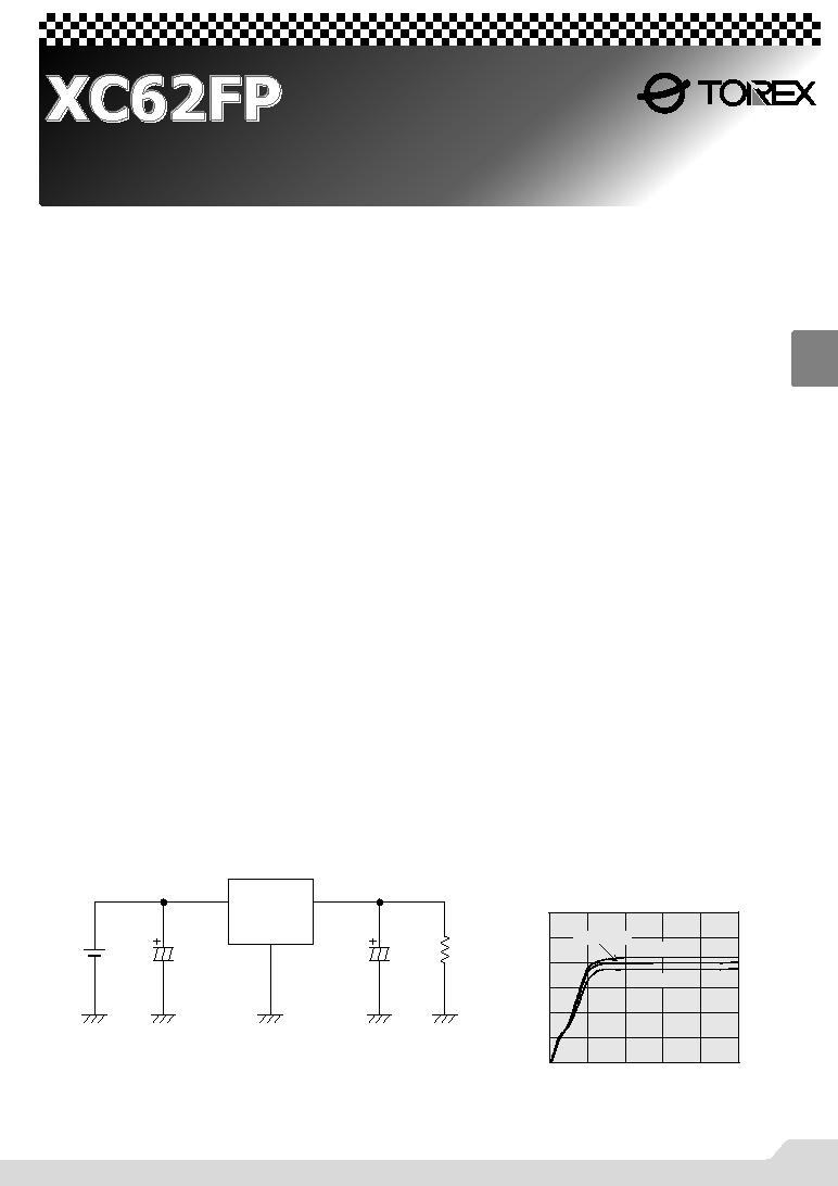
Topr=25
85
-40
XC62FP3002 (3V)
Supply Current:Iss (
µ
A)
Input Voltage:V
IN
(V)
General Description
Features
Applications
Typical Application Circuit
Typical Performance
Characteristic
03S_05XC62FP 02.10.7 5:18 PM 285
XC62FP
Series
286
3
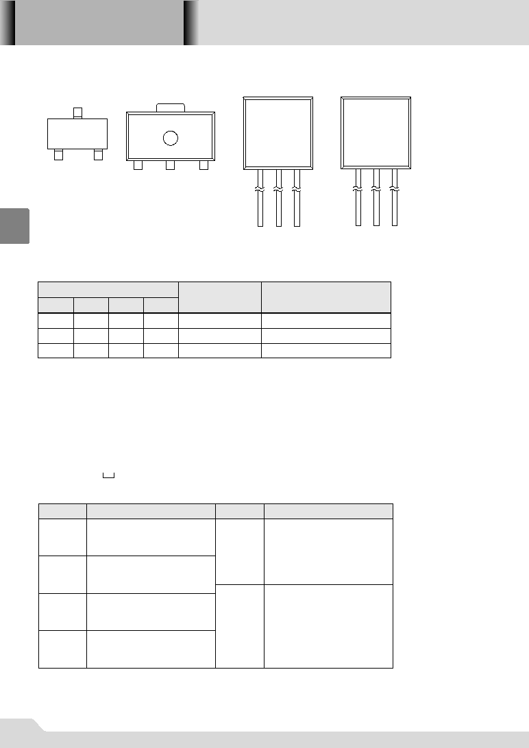
SOT-23
TOP VIEW
SOT-89
TOP VIEW
3
1
2
V
OUT
V
SS
SS
V
OUT
V
IN
V
IN
1
2
3
PIN NUMBER
SOT-23
SOT-89
FUNCTION
1
1
Supply voltage input
Ground
Regulated voltage output
3
2
2
3
TO-92 (L)
PIN NAME
2
1
3
TO-92 (T)
1
2
3
V
IN
V
SS
V
OUT
Product Classification
GOrdering Information
DESIGNATOR
a
e
f
b
c
d
DESCRIPTION
DESIGNATOR
DESCRIPTION
Polarity of Output Voltage:
P: + (Positive)
Temperature Coefficients:
0=
±100ppm (typical)
Output Voltage
30=3.0V
50=5.0V
Output Voltage Accuracy:
1=
±1.0% (Semi-custom)
2=
±2.0%
Package Type
M=SOT-23
P=SOT-89
T=TO-92 (Standard)
L=TO-92 (Custom pin configuration)
Device Orientation
R=Embossed Tape
(Standard Feed)
L=Embossed Tape
(Reverse Feed)
H=Paper Tape (TO-92)
B=Bag (TO-92)
X C 6 2 F X X X X X X X
a
b
c
d
e
f
1
2
3
TO-92T Type
TOP VIEW
V
IN
V
OUT
V
SS
1
2
3
TO-92 (L Type)
TOP VIEW
V
IN
V
SS
V
OUT
Pin Configuration
Pin Assignment
03S_05XC62FP 02.9.12 3:01 PM 286

GSOT-89
1.1±0.1
00.1
0.15
0.95
1.9±0.2
2.9±0.2
0.2min
2.8±0.2
+0.1
-0.05
0.4
+0.1
-0.05
1.6
+0.2
-0.1
4.5±0.1
0.4
2.5±0.1
0.8
min
4.25max
0.42±0.06
0.4
1.5±0.1
0.47±0.06
1.5±0.1
0.42±0.06
1.5±0.1
1.6
+0.15
-0.2
+0.03
-0.02
XC62FP
Series
287
3
Packaging Information
GSOT-23
03S_05XC62FP 02.9.12 3:01 PM 287

XC62FP
Series
288
3
Marking
GSOT-23, SOT-89
q Represents the integer of the Output Voltage
SYMBOL
VOLTAGE(V)
2
2.w
1
1.w
4
4.w
3
3.w
SYMBOL
VOLTAGE(V)
6
6.w
5
5.w
w Represents the decimal number of the Output Voltage
SYMBOL
VOLTAGE(V)
SYMBOL
VOLTAGE(V)
B
q.1
H
A
q.0
F
D
q.3
L
q.8
C
q.2
q.6
q.5
q.7
K
E
q.4
M
q.9
r Represents the assembly lot no.
Based on internal standards
SYMBOL
0
e Based on internal standards
SOT-23
TOP VIEW
SOT-89
TOP VIEW
1 2 3 4
1
2
3
4
GTO-92
3.7±0.3
10.0min
1.6±0.1
0.4±0.05
4.65
0.45±0.1
2.5
+0.4
-0.1
2.5
+0.4
-0.1
+0.35
-0.45
4.8
+0.4
-0.5
03S_05XC62FP 02.9.12 3:01 PM 288
Absolute Maximum Ratings
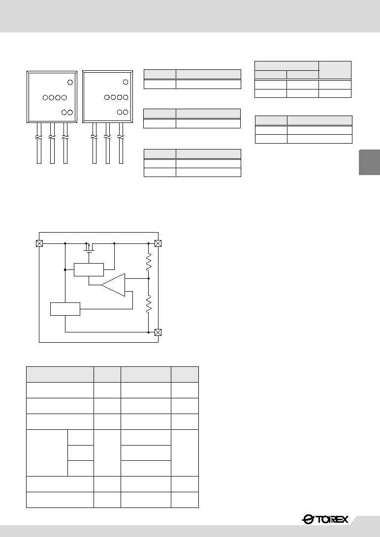
Block Diagram
V
OUT
V
IN
V
SS
+
-
Current
Limit
Voltage
Reference
PARAMETER
Input Voltage
Output Voltage
Output Current
SOT-23
Continuous
Total Power
Dissipation
SOT-89
Operating Ambient
Temperature
Storage Temperature
RATINGS
12
500
150
500
TO-92
300
≠40 ~ +85
≠40 ~ +125
UNITS
V
V
mA
mW
∞C
∞C
SYMBOL
V
IN
V
OUT
I
OUT
P
d
T
opr
T
stg
Ta=25
∞C
V
SS
-0.3 ~ V
IN
+0.3
GTO-92
2 3 4 5
6 7
1
TO-92L Type
(TOP VIEW)
62F
L
2 3 4 5
6 7
1
TO-92T Type
(TOP VIEW)
62F
q Represents the polarity of
Output Voltage
DESIGNATOR
CONFIGURATION
P
CMOS
we Represents the Detect Voltage
w
3
3.3
5
5.0
e
DESIGNATOR
VOLTAGEV
3
0
r Represents the temperature
characteristics
DESIGNATOR TEMPERATURE CHARACTERISTICS
0
TPY±100ppm
DESIGNATOR DETECT VOLTAGE ACCURACY
1
within ±1semi-custom
2
within ±2
t Represents the Detect
Voltage Accuracy
y Represents a least significant
digit of the produced year
DESIGNATOR
PRODUCED YEAR
0
2000
1
2001
u Denotes the production lot number
0 to 9, A to Z repeated (G.I.J.O.Q.W excepted)
XC62FP
Series
289
3
03S_05XC62FP 02.9.12 3:01 PM 289

XC62FP
Series
290
3
Electrical Characteristics
Ta=25
∞C
XC62FP5002 V
OUT
(T)=5.0V
(Note1)
PARAMETER
SYMBOL
CONDITIONS
Output Voltage
V
OUT
(E)
(Note2)
I
OUT
=40mA
V
IN
=6.0V
Load Stability
V
OUT
Input -Output
Voltage Differential
(Note3)
Maximum Output Current
I
OUT
max
V
IN
=6.0V, V
OUT
(E)
4.5V
V
IN
=6.0V
1mA
I
OUT
100mA
Ta=25
∞C
XC62FP4002 V
OUT
(T)=4.0V
(Note1)
PARAMETER
SYMBOL
CONDITIONS
Output Voltage
V
OUT
(E)
(Note2)
I
OUT
=40mA
V
IN
=5.0V
Load Stability
V
OUT
Input -Output
Voltage Differential
(Note3)
Maximum Output Current
I
OUT
max
V
IN
=5.0V, V
OUT
(E)
3.6V
V
IN
=5.0V
1mA
I
OUT
100mA
MIN
4.900
2.0
250
TYP
5.000
40
80
MAX
5.100
4.5
UNITS
V
mV
µA
mA
CIRCUIT
1
1
0.2
0.3
%/V
1
2
1
120
300
mV
1
Vdif1
I
OUT
=100mA
600
380
mV
1
Vdif2
I
OUT
=200mA
V
IN
=6.0V
Supply Current
I
SS
10
V
--
Input Voltage
V
IN
Input Stability
I
OUT
=40mA
6.0V
V
IN
10.0V
V
OUT
V
IN
∑
V
OUT
±100
ppm/
∞C
1
Output Voltage
Temperature Characteristics
I
OUT
=40mA
-40
∞C Topr 85∞C
V
OUT
Topr
∑
V
OUT
MIN
3.920
2.0
200
TYP
4.000
45
90
MAX
4.080
4.5
UNITS
V
mV
µA
mA
CIRCUIT
1
1
0.2
0.3
%/V
1
2
1
170
330
mV
1
Vdif1
I
OUT
=100mA
630
400
mV
1
Vdif2
I
OUT
=200mA
V
IN
=5.0V
Supply Current
I
SS
10
V
--
Input Voltage
V
IN
Input Stability
I
OUT
=40mA
5.0V
V
IN
10.0V
V
OUT
V
IN
∑
V
OUT
±100
ppm/
∞C
1
Output Voltage
Temperature Characteristics
I
OUT
=40mA
-40
∞C Topr 85∞C
V
OUT
Topr
∑
V
OUT
03S_05XC62FP 02.9.12 3:01 PM 290

Ta=25
∞C
XC62FP3002 V
OUT
(T)=3.0V
(Note1)
PARAMETER
SYMBOL
CONDITIONS
Output Voltage
V
OUT
(E)
(Note2)
I
OUT
=40mA
V
IN
=4.0V
Load Stability
V
OUT
Input -Output
Voltage Differential
(Note3)
Maximum Output Current
I
OUT
max
V
IN
=4.0V, V
OUT
(E)
2.7V
V
IN
=4.0V
1mA
I
OUT
80mA
Ta=25
∞C
XC62FP2002 V
OUT
(T)=2.0V
(Note1)
PARAMETER
SYMBOL
CONDITIONS
Output Voltage
V
OUT
(E)
(Note2)
I
OUT
=40mA
V
IN
=3.0V
Load Stability
V
OUT
Input -Output
Voltage Differential
(Note3)
Maximum Output Current
I
OUT
max
V
IN
=3.0V, V
OUT
(E)
1.8V
V
IN
=3.0V
1mA
I
OUT
60mA
MIN
2.940
2.0
150
TYP
3.000
45
90
MAX
3.060
4.5
UNITS
V
mV
µA
mA
CIRCUIT
1
1
0.2
0.3
%/V
1
2
1
180
360
mV
1
Vdif1
I
OUT
=80mA
700
400
mV
1
Vdif2
I
OUT
=160mA
V
IN
=4.0V
Supply Current
I
SS
10
V
--
Input Voltage
V
IN
Input Stability
I
OUT
=40mA
4.0V
V
IN
10.0V
V
OUT
V
IN
∑
V
OUT
±100
ppm/
∞C
1
Output Voltage
Temperature Characteristics
I
OUT
=40mA
-40
∞C
Topr
85∞C
V
OUT
Topr
∑
V
OUT
MIN
1.960
2.0
100
TYP
2.000
45
90
MAX
2.040
4.5
UNITS
V
mV
µA
mA
CIRCUIT
1
1
0.2
0.3
%/V
1
2
1
180
360
mV
1
Vdif1
I
OUT
=60mA
700
400
mV
1
Vdif2
I
OUT
=120mA
V
IN
=3.0V
Supply Current
I
SS
10
V
--
Input Voltage
V
IN
Input Stability
I
OUT
=40mA
3.0V
V
IN
10.0V
V
OUT
V
IN
∑
V
OUT
±100
ppm/
∞C
1
Output Voltage
Temperature Characteristics
I
OUT
=40mA
-40
∞C
Topr
85∞C
V
OUT
Topr
∑
V
OUT
1. V
OUT
(T)=Specified Output Voltage .
2. V
OUT
(E)=Effective Output Voltage (i.e. the output voltage when "V
OUT
(T)+1.0V" is provided at the V
IN
pin while maintaining a certain I
OUT
value).
3. Vdif= {V
IN
1
(Note4)
-V
OUT
(E)}
4. V
IN
1= The input voltage at the time 98% of V
OUT
(E) is output (input voltage has been gradually reduced).
Note:
XC62FP
Series
291
3
03S_05XC62FP 02.9.12 3:01 PM 291

XC62FP
Series
292
3
Typical Application Circuit
GStandard Circuit
Directions for use
V
IN
V
IN
V
OUT
V
ss
R
L
C
IN
1
µF
Tantalum
C
L
1
µF
Tantalum
GNotes on Use
1. Please use this IC within the stipulated absolute maximum ratings as the IC is liable to malfunction outside of such parameters.
2. There is a possibility that oscillation may occur as a result of the impedance present between the power supply and the IC's input. Where
impedance is 10
or more, please use a capacitor (C
IN
) of at least 1
µF.
With a large output current, operations can be stabilised by increasing capacitor size (C
IN
). If C
IN
is small and capacitor size (C
L
) is
increased, there is a possibility of oscillation due to input impedance.
In such cases, operations can be stabilised by either increasing the size of C
IN
or decreasing the size of C
L
.
3. Please ensure that output current (I
OUT
) is less than Pd ˜ (V
IN
-V
OUT
) and does not exceed the stipulated Continuous Total Power Dissipation
value (Pd) for the package.
4. Should you wish to increase output current (I
OUT
) and/or have the capability to exceed the stipulated Pd value, using a current boost circuit
(similar to the one shown below) is likely to lead to oscillation.
With such applications, we recommend use of a boost type voltage regulator, such as the Torex XC62EP series.
Current Boost Circuit : Poor Example
V
IN
V
OUT
V
ss
R
BE
IN
OUT
XC62FP
PNP Tr
C
IN
Tantalum
C
L
Tantalum
03S_05XC62FP 02.9.12 3:01 PM 292
Test Circuits
Circuit 1
V
IN
V
IN
V
SS
V
OUT
A
V
1F
Tantalum
1F
Tantalum
Circuit 2
V
IN
OPEN
V
IN
V
SS
V
OUT
A
XC62FP
Series
293
3
03S_05XC62FP 02.9.12 3:01 PM 293
XC62FP
Series
294
3
Typical Performance Characteristics
4.7
4.8
4.9
5.0
5.1
0
20
40
60
80 100 120 140 160 180
Topr=25
85
-40
2.7
2.8
2.9
3.0
3.1
0
20
40
60
80 100 120 140 160 180
Topr=25
85
-40
1.7
1.8
1.9
2.0
2.1
0
20
40
60
80
100
120
Topr=-40,25
85
3.7
3.8
3.9
4.0
4.1
0
20
40
60
80 100 120 140 160 180
Topr=25
85
-40
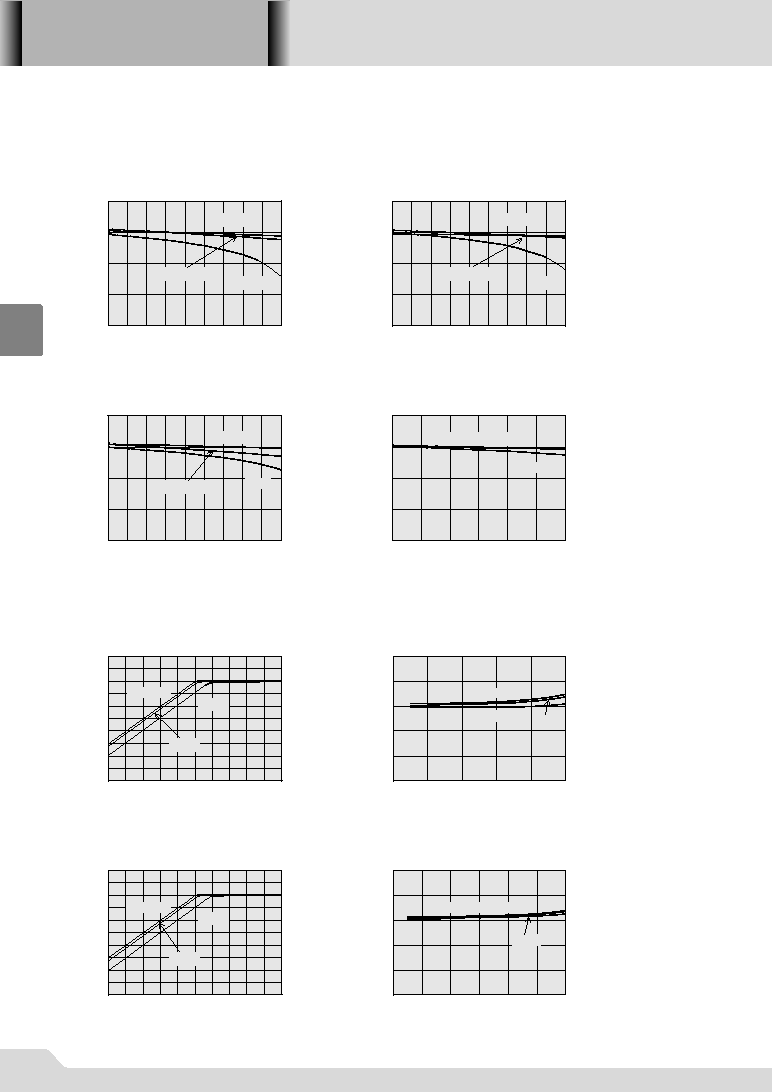
(1) OUTPUT VOLTAGE vs. OUTPUT CURRENT
XC62FP5002 (5V)
V
IN
=6V
C
IN
=1
µF(tantalum), C
L
=1
µF(tantalum)
XC62FP4002 (4V)
V
IN
=5V
C
IN
=1
µF(tantalum), C
L
=1
µF(tantalum)
Output Voltage:V
OUT
(V)
Output Voltage:V
OUT
(V)
XC62FP3002 (3V)
XC62FP2002 (2V)
C
IN
=1
µF(tantalum), C
L
=1
µF(tantalum)
V
IN
=4V
C
IN
=1
µF(tantalum), C
L
=1
µF(tantalum)
V
IN
=3V
Output Voltage:V
OUT
(V)
Output Voltage:V
OUT
(V)
Output Current:I
OUT
(mA)
Output Current:I
OUT
(mA)
Output Current:I
OUT
(mA)
Output Current:I
OUT
(mA)
3.2
3.4
3.6
3.8
4.0
4.2
3.5
4.0
4.5
Topr=25
I
OUT
=1mA
40mA
10mA
3.85
3.90
3.95
4.00
4.05
4.10
4
5
6
7
8
9
10
I
OUT
=1mA10mA
Topr=25
40mA
4.2
4.4
4.6
4.8
5.0
5.2
4.5
5.0
5.5
XC62FP5002 (5V)
Topr=25
40mA
10mA
4.85
4.90
4.95
5.00
5.05
5.10
5
6
7
8
9
10
I
OUT
=1mA
Topr=25
40mA
10mA
(2) OUTPUT VOLTAGE vs. INPUT VOLTAGE
XC62FP5002 (5V)
XC62FP4002 (4V)
XC62FP4002 (4V)
Output Voltage:V
OUT
(V)
Output Voltage:V
OUT
(V)
Output Voltage:V
OUT
(V)
Output Voltage:V
OUT
(V)
Input Voltage:V
IN
(V)
Input Voltage:V
IN
(V)
Input Voltage:V
IN
(V)
Input Voltage:V
IN
(V)
C
IN
=1
µF(tantalum), C
L
=1
µF(tantalum)
C
IN
=1
µF(tantalum), C
L
=1
µF(tantalum)
C
IN
=1
µF(tantalum), C
L
=1
µF(tantalum)
C
IN
=1
µF(tantalum), C
L
=1
µF(tantalum)
I
OUT
=1mA
03S_05XC62FP 02.9.12 3:01 PM 294
2.2
2.4
2.6
2.8
3.0
3.2
2.5
3.0
3.5
Topr=25
I
OUT
=1mA
40mA
10mA
2.85
2.90
2.95
3.00
3.05
3.10
3
4
5
6
7
8
9
10
I
OUT
=1mA
Topr=25
40mA
10mA
XC62FP3002 (3V)
XC62FP3002 (3V)
Output Voltage:V
OUT
(V)
Output Voltage:V
OUT
(V)
Input Voltage:V
IN
(V)
Input Voltage:V
IN
(V)
C
IN
=1
µF(tantalum), C
L
=1
µF(tantalum)
C
IN
=1
µF(tantalum), C
L
=1
µF(tantalum)
(2) OUTPUT VOLTAGE vs. INPUT VOLTAGE
(3) INPUT/OUTPUT VOLTAGE DIFFERENTIAL vs. OUTPUT CURRENT
1.85
1.90
1.95
2.00
2.05
2.10
2
3
4
5
6
7
8
9
10
1mA,10mA
I
OUT
=40mA
Topr=25
-0.2
0.0
0.2
0.4
0.6
0.8
1.0
0
20
40
60
80 100 120 140 160 180
Input/Output Voltage Diff.: Vdif (V)
Input/Output Voltage Diff.: Vdif (V)
Input/Output Voltage Diff.: Vdif (V)
Input/Output Voltage Diff.: Vdif (V)
Topr=25
85
-40
-0.2
0.0
0.2
0.4
0.6
0.8
1.0
0
20
40
60
80 100 120 140 160 180
Topr=25
85
-40
-0.2
0.0
0.2
0.4
0.6
0.8
1.0
0
20
40
60
80
100
120
Topr=25
85
-40
1.2
1.3
1.4
1.5
1.6
1.7
1.8
1.9
2.0
2.1
2.2
1.5
2.0
2.5
I
OUT
=40mA
1mA
10mA
Topr=25
-0.2
0.0
0.2
0.4
0.6
0.8
1.0
0
20
40
60
80 100 120 140 160 180
Topr=25
85
-40
XC62FP3002 (3V)
XC62FP2002 (2V)
XC62FP5002 (5V)
XC62FP4002 (4V)
XC62FP2002 (2V)
XC62FP2002 (2V)
Input Voltage:V
IN
(V)
Output Voltage:V
OUT
(V)
C
IN
=1
µF(tantalum), C
L
=1
µF(tantalum)
C
IN
=1
µF(tantalum), C
L
=1
µF(tantalum)
C
IN
=1
µF(tantalum), C
L
=1
µF(tantalum)
C
IN
=1
µF(tantalum), C
L
=1
µF(tantalum)
C
IN
=1
µF(tantalum), C
L
=1
µF(tantalum)
C
IN
=1
µF(tantalum), C
L
=1
µF(tantalum)
Output Current:I
OUT
(mA)
Output Current:I
OUT
(mA)
Output Current:I
OUT
(mA)
Output Current:I
OUT
(mA)
Input Voltage:V
IN
(V)
Output Voltage:V
OUT
(V)
XC62FP
Series
295
3
03S_05XC62FP 02.9.12 3:01 PM 295
XC62FP
Series
296
3
0
1
2
3
0
2
4
6
8
10
Topr=25
85
-40
1.50
1.75
2.00
2.25
2.50
3
4
5
6
7
8
9
10
Topr=25
85
-40
0
1
2
3
0
2
4
6
8
10
Topr=25
85
-40
1.50
1.75
2.00
2.25
2.50
4
5
6
7
8
9
10
Topr=25
85
-40
0
1
2
3
0
2
4
6
8
10
Topr=25
85
-40
1.50
1.75
2.00
2.25
2.50
5
6
7
8
9
10
Topr=25
85
-40
(4) SUPPLY CURRENT vs. INPUT VOLTAGE
XC62FP5002 (5V)
XC62FP5002 (5V)
XC62FP4002 (4V)
XC62FP4002 (4V)
XC62FP3002 (3V)
XC62FP3002 (3V)
Input Voltage:V
IN
(V)
Supply Current:Iss (
µ
A)
Supply Current:Iss (
µ
A)
Supply Current:Iss (
µ
A)
Supply Current:Iss (
µ
A)
Supply Current:Iss (
µ
A)
Supply Current:Iss (
µ
A)
Input Voltage:V
IN
(V)
Input Voltage:V
IN
(V)
Input Voltage:V
IN
(V)
Input Voltage:V
IN
(V)
Input Voltage:V
IN
(V)
1.50
1.75
2.00
2.25
2.50
2
4
6
8
10
Topr=25
-40
85
0
1
2
3
0
2
4
6
8
10
Topr=25
-40
85
XC62FP2002 (2V)
XC62FP2002 (2V)
Supply Current:Iss (
µ
A)
Supply Current:Iss (
µ
A)
Input Voltage:V
IN
(V)
Input Voltage:V
IN
(V)
03S_05XC62FP 02.9.12 3:01 PM 296

1.90
1.95
2.00
2.05
2.10
-40
-20
0
20
40
60
80
100
40mA
3.90
3.95
4.00
4.05
4.10
-40
-20
0
20
40
60
80
100
40mA
4.90
4.95
5.00
5.05
5.10
-40
-20
0
20
40
60
80
100
Ambient Temp.:Topr ()
Ambient Temp.:Topr ()
Ambient Temp.:Topr ()
Ambient Temp.:Topr ()
Ambient Temp.:Topr ()
Ambient Temp.:Topr ()
Ambient Temp.:Topr ()
Ambient Temp.:Topr ()
40mA
2.90
2.95
3.00
3.05
3.10
-40
-20
0
20
40
60
80
100
40mA
(5) OUTPUT VOLTAGE vs. AMBIENT TEMPERATURE
XC62FP5002 (5V)
XC62FP4002 (4V)
XC62FP2002 (2V)
XC62FP3002 (3V)
V
IN
=6V
V
IN
=6V
V
IN
=4V
V
IN
=3V
C
IN
=1
µF(tantalum), C
L
=1
µF(tantalum)
C
IN
=1
µF(tantalum), C
L
=1
µF(tantalum)
C
IN
=1
µF(tantalum), C
L
=1
µF(tantalum)
C
IN
=1
µF(tantalum), C
L
=1
µF(tantalum)
Output Voltage:V
OUT
(V)
Output Voltage:V
OUT
(V)
Output Voltage:V
OUT
(V)
Output Voltage:V
OUT
(V)
I
OUT
=10mA
I
OUT
=10mA
I
OUT
=10mA
I
OUT
=10mA
1.0
1.5
2.0
2.5
3.0
-40
-20
0
20
40
60
80
100
1.0
1.5
2.0
2.5
3.0
-40
-20
0
20
40
60
80
100
1.0
1.5
2.0
2.5
3.0
-40
0
-20
20
40
60
80
100
1.0
1.5
2.0
2.5
3.0
-40
-20
0
20
40
60
80
100
(6) SUPPLY CURRENT vs. AMBIENT TEMPERATURE
XC62FP5002 (5V)
XC62FP4002 (4V)
V
IN
=5V
V
IN
=6V
Supply Current:Iss (
µ
A)
Supply Current:Iss (
µ
A)
Supply Current:Iss (
µ
A)
Supply Current:Iss (
µ
A)
XC62FP2002 (2V)
XC62FP3002 (3V)
V
IN
=4V
V
IN
=3V
XC62FP
Series
297
3
03S_05XC62FP 02.9.12 3:01 PM 297

XC62FP
Series
298
3
(7) INPUT TRANSIENT RESPONSE 1
-8
-6
-4
-2
0
2
4
6
8
Time(0.4msec/div)
0
1
2
3
4
5
6
7
8
Output Voltage
Input Voltage
-8
-6
-4
-2
0
2
4
6
8
Time(0.4msec/div)
0
1
2
3
4
5
6
7
8
Input Voltage:V
IN
(V)
Input Voltage:V
IN
(V)
Output Voltage:V
OUT
(V)
Output Voltage:V
OUT
(V)
XC62FP5002 (5V)
XC62FP5002 (5V)
I
OUT
=1mA, C
L
=1
µF(tantalum)
I
OUT
=10mA, C
L
=1
µF(tantalum)
-6
-4
-2
0
2
4
6
Time(0.4msec/div)
0
1
2
3
4
5
6
-8
-6
-4
-2
0
2
4
6
8
Time(0.4msec/div)
0
1
2
3
4
5
6
7
8
-8
-6
-4
-2
0
2
4
6
8
Time(0.4msec/div)
0
1
2
3
4
5
6
7
8
-6
-4
-2
0
2
4
6
Time(0.4msec/div)
0
1
2
3
4
5
6
-6
-4
-2
0
2
4
6
Time(0.4msec/div)
0
1
2
3
4
5
6
-6
-4
-2
0
2
4
6
Time(0.4msec/div)
0
1
2
3
4
5
6
XC62FP4002 (4V)
XC62FP4002 (4V)
I
OUT
=10mA, C
L
=1
µF(tantalum)
I
OUT
=1mA, C
L
=1
µF(tantalum)
XC62FP3002 (3V)
XC62FP3002 (3V)
XC62FP2002 (2V)
XC62FP2002 (2V)
I
OUT
=10mA, C
L
=1
µF(tantalum)
I
OUT
=1mA, C
L
=1
µF(tantalum)
I
OUT
=1mA, C
L
=1
µF(tantalum)
I
OUT
=10mA, C
L
=1
µF(tantalum)
Input Voltage:V
IN
(V)
Output Voltage:V
OUT
(V)
Input Voltage:V
IN
(V)
Output Voltage:V
OUT
(V)
Input Voltage:V
IN
(V)
Output Voltage:V
OUT
(V)
Input Voltage:V
IN
(V)
Output Voltage:V
OUT
(V)
Output Voltage:V
OUT
(V)
Input Voltage:V
IN
(V)
Output Voltage:V
OUT
(V)
Input Voltage:V
IN
(V)
Output Voltage
Input Voltage
Output Voltage
Input Voltage
Output Voltage
Input Voltage
Output Voltage
Input Voltage
Output Voltage
Input Voltage
Output Voltage
Input Voltage
Output Voltage
Input Voltage
03S_05XC62FP 02.9.12 3:01 PM 298

(8) INPUT TRANSIENT RESPONSE 2
1
2
3
4
5
6
2.5
3.0
3.5
4.0
4.5
5.0
3
4
5
6
7
8
4.5
5.0
5.5
6.0
6.5
7.0
1
2
3
4
5
6
2.5
3.0
3.5
4.0
4.5
5.0
2
3
4
5
6
7
3.5
4.0
4.5
5.0
5.5
6.0
2
3
4
5
6
7
3.5
4.0
4.5
5.0
5.5
6.0
3
4
5
6
7
8
4.5
5.0
5.5
6.0
6.5
7.0
Time (1msec/div)
Time (1msec/div)
Time (1msec/div)
Time (1msec/div)
Time (1msec/div)
Time (1msec/div)
XC62FP5002 (5V)
XC62FP5002 (5V)
XC62FP4002 (4V)
XC62FP4002 (4V)
XC62FP3002 (3V)
XC62FP3002 (3V)
I
OUT
=1mA,C
L
=1
µF(tantalum)
I
OUT
=10mA,C
L
=1
µF(tantalum)
Output
Voltage:V
OUT
(V)
Input Voltage:V
IN
(V)
Output
Voltage:V
OUT
(V)
Input Voltage:V
IN
(V)
Output
Voltage:V
OUT
(V)
Input Voltage:V
IN
(V)
Output
Voltage:V
OUT
(V)
Input Voltage:V
IN
(V)
Output
Voltage:V
OUT
(V)
Input Voltage:V
IN
(V)
Output
Voltage:V
OUT
(V)
Input Voltage:V
IN
(V)
Output
Voltage:V
OUT
(V)
Input Voltage:V
IN
(V)
Output
Voltage:V
OUT
(V)
Input Voltage:V
IN
(V)
I
OUT
=10mA,C
L
=1
µF(tantalum)
I
OUT
=10mA,C
L
=1
µF(tantalum)
I
OUT
=1mA,C
L
=1
µF(tantalum)
I
OUT
=1mA,C
L
=1
µF(tantalum)
0
1
2
3
4
5
1.5
2.0
2.5
3.0
3.5
4.0
0
1
2
3
4
5
1.5
2.0
2.5
3.0
3.5
4.0
XC62FP2002 (2V)
XC62FP2002 (2V)
Time (1msec/div)
Time (1msec/div)
I
OUT
=1mA,C
L
=1
µF(tantalum)
I
OUT
=10mA,C
L
=1
µF(tantalum)
Output Voltage
Input Voltage
Output Voltage
Input Voltage
Output Voltage
Input Voltage
Output Voltage
Input Voltage
Output Voltage
Input Voltage
Output Voltage
Input Voltage
Output Voltage
Input Voltage
Output Voltage
Input Voltage
XC62FP
Series
299
3
03S_05XC62FP 02.9.12 3:01 PM 299

XC62FP
Series
300
3
-1
0
1
2
3
4
0
40
80
120
160
200
1mA
40mA
0
1
2
3
4
5
0
40
80
120
160
200
1mA
40mA
1
2
3
4
5
6
0
40
80
120
160
200
1mA
40mA
2
3
4
5
6
7
0
40
80
120
160
200
Output Voltage
Output Current
Output Voltage
Output Current
Output Voltage
Output Current
Output Voltage
Output Current
1mA
40mA
XC62FP4002 (4V)
XC62FP5002 (5V)
XC62FP2002 (2V)
XC62FP3002 (3V)
Output Voltage:V
OUT
(V)
Output Current:I
OUT
(mA)
Output Voltage:V
OUT
(V)
Output Current:I
OUT
(mA)
Output Voltage:V
OUT
(V)
Output Current:I
OUT
(mA)
Output Voltage:V
OUT
(V)
Output Current:I
OUT
(mA)
Time (2msec/div)
Time (2msec/div)
Time (2msec/div)
Time (2msec/div)
V
IN
=4V, C
L
=1
µF(tantalum)
V
IN
=3V, C
L
=1
µF(tantalum)
V
IN
=5V, C
L
=1
µF(tantalum)
V
IN
=6V, C
L
=1
µF(tantalum)
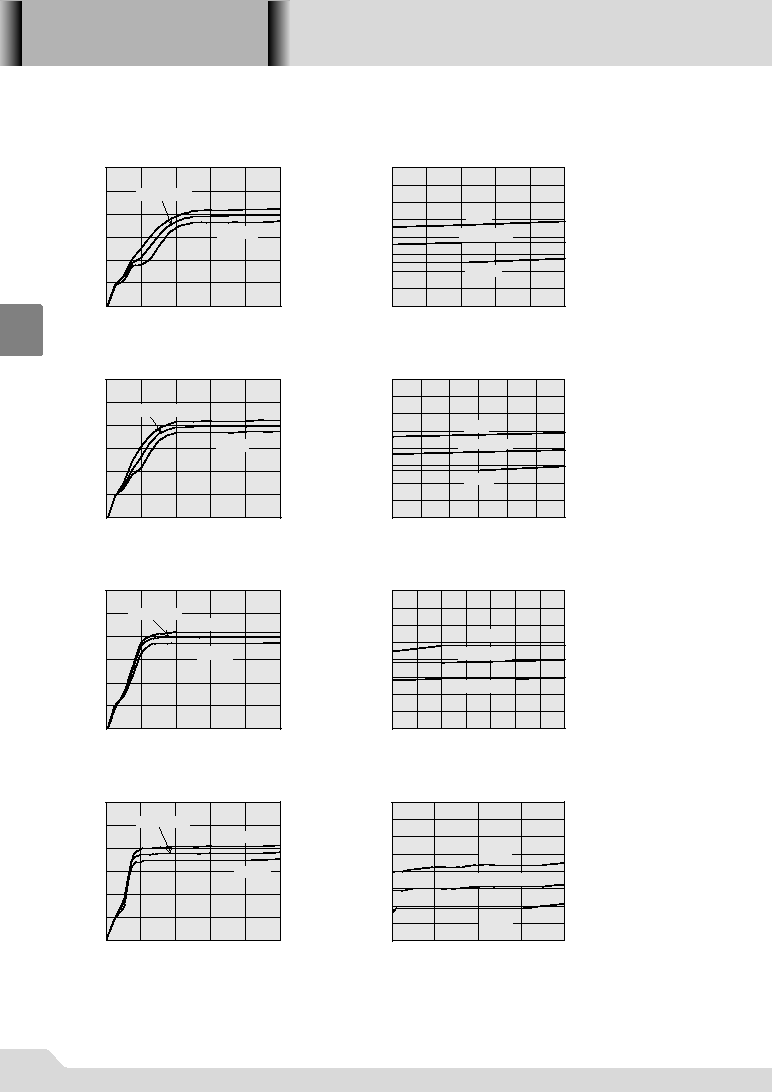
(9) LOAD TRANSIENT RESPONSE
0
10
20
20
30
40
50
60
0.01
0.1
1
10
0
10
20
30
40
50
60
0.01
0.1
1
10
0
10
30
40
50
60
0.01
0.1
1
10
0
10
20
30
40
50
60
0.01
0.1
1
10
(10) RIPPLE REJECTION RATE
XC62FP5002 (5V)
XC62FP4002 (4V)
V
IN
=5V
DC
+1Vp-pAC
I
OUT
=40mA, C
L
=1
µF(tantalum)
V
IN
=6V
DC
+1Vp-pAC
I
OUT
=40mA, C
L
=1
µF(tantalum)
V
IN
=3V
DC
+1Vp-pAC
V
IN
=4V
DC
+1Vp-pAC
I
OUT
=40mA, C
L
=1
µF(tantalum)
I
OUT
=40mA, C
L
=1
µF(tantalum)
XC62FP2002 (2V)
XC62FP3002 (3V)
Ripple Rejection Rate:RR (dB)
Ripple Rejection Rate:RR (dB)
Ripple Rejection Rate:RR (dB)
Ripple Rejection Rate:RR (dB)
Ripple Frequency:f (kHz)
Ripple Frequency:f (kHz)
Ripple Frequency:f (kHz)
Ripple Frequency:f (kHz)
03S_05XC62FP 02.9.12 3:01 PM 300