w
-44
s
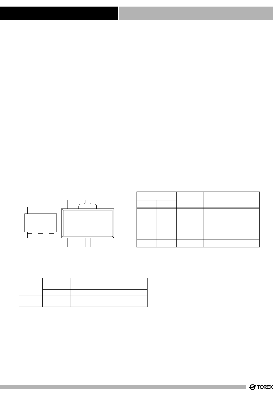
Pin Configuration
x
CMOS Low Power Consumption
x
Small Input-Output Voltage Differential:
0.18V at 60mA, 0.58V at 160mA
x
Maximum Output Current: 165mA (V
OUT
=3.0V)
x
Highly Accurate:
±
2%(
±
1%)
x
Output Voltage Range: 2.0V~6.0V
x
Standby Supply Current 0.1
µ
A(V
OUT
=3.0V)
x
SOT-25/SOT-89-5 Package
s
Applications
q
Battery Powered Instruments
q
Voltage supplies for cellular phones
q
Cameras and Video Recorders
q
Palmtops
s
Pin Assignment
XC62HR Series
Positive Voltage Regulators
CE
V
IN
V
SS
V
OUT
(NC)
V
OUT
(NC)
V
IN
CE
V
SS
4
5
5
4
3
2
1
1
2
3
SOT-89-5
(TOP VIEW)
SOT-25
(TOP VIEW)
Preliminary
Output On/Off Control
s
Function
H=High, L=Low
SERIES
CE
VOLTAGE OUTPUT
XC62HR
H
ON
L
OFF
XC62HP
H
OFF
L
ON
PIN NUMBER
SOT-25
SOT-89-5
PIN NAME
FUNCTION
1
4
No Connection
Supply Voltage Input
Chip Enable
2
2
3
3
(NC)
V
IN
CE
Ground
Regulated Output Voltage
4
1
5
5
V
SS
V
OUT
s
General Description
The XC62H series are highly precise, low power consumption, positive
voltage regulators, manufactured using CMOS and laser trimming
technologies. The series consists of a high precision voltage reference, an
error correction circuit, and an output driver with current limitation.
By way of the CE function, with output turned off, the series enters stand-
by. In the stand-by mode, power consumption is greatly reduced.
SOT-25 (150mW) and SOT-89-5 (500mW) packages are available.
In relation to the CE function, as well as the positive logic XC62HR series,
a negative logic XC62HP series (custom) is also available.
s
Features
Maximum Output Current: 165mA (within Maximum power dissipation,
V
OUT
=3.0V)
Output Voltage Range: 2.0V ~ 6.0V in 0.1V increments
(1.1V to 1.9V semi-custom)
Highly Accurate: Set-up Voltage
±
2% (
±
1% for semi-custom products)
Low power consumption: TYP 3.0
µ
A (V
OUT
=3.0, Output enabled)
TYP 0.1
µ
A (Output disabled)
Output voltage temperature characteristics: TYP
±
100ppm/
:
Input stability: TYP 0.2%/V
Ultra small package: SOT-25 (150mW) mini-mold
SOT-89-5 (500mW) mini-power mold
HP010199
75

s
Block Diagram
V
IN
V
OUT
V
SS
CE
Voltage
Reference
Output
Control
Current
Limit
+
--
s
Absolute Maximum Ratings
s
Standard Circuit
Ta=25
:
PARAMETER
RATINGS
UNITS
SYMBOL
Input Voltage
12
V
V
IN
Output Current
500
mA
I
OUT
Output Voltage
VSS-0.3 ~ V
IN
+0.3
V
V
OUT
CE Input Voltage
VSS-0.3 ~ V
IN
+0.3
V
VCE
Continuous Total
Power Dissipation
150
Pd
500
mW
Pd
SOT-25
SOT-89-5
Operating Ambient Temperature
-30 ~ +80
:
Topr
Storage Temperature
-40 ~ +25
:
Tstg
Note: I
OUT
must be less than Pd / (V
IN
-V
OUT
).
V
SS
CE
V
IN
V
IN
R
L
C
L
1
µ
F
(Tantalum)
C
IN
1
µ
F
(Tantalum)
V
OUT
w
-45
XC62HR Series
Positive Voltage Regulators
76

s
Electrical Characteristics
Ta=25
:
XC62HR2002 V
OUT
(T)=2.0V(Note1)
PARAMETER
SYMBOL
CONDITIONS
Output Voltage
V
OUT
(E)
(Note2)
I
OUT
=40mA
V
IN
=3.0V
Load Stability
V
OUT
Input -Output
Voltage Differential (Note3)
Maximum Output Current
I
OUT
max
V
IN
=3.0V, V
OUT
(E)
1.8V
CE "High" Current
ICEH
V
CE
=V
IN
CE "Low" Current
ICEL
V
CE
=V
SS
V
IN
=3.0V
1mA
I
OUT
60mA
w
-46
MIN
1.960
2.9
115
TYP
2.000
45
90
-0.05
MAX
2.040
7.9
5.0
0
UNITS
V
mV
µ
A
mA
µ
A
µ
A
CIRCUIT
1
1
0.2
0.3
%/V
1
2
1
2
2
180
360
mV
1
Vdif1
I
OUT
=40mA
880
580
mV
1
Vdif2
I
OUT
=100mA
V
IN
=V
CE
=3.0V
Supply Current1
ISS1
10.0
V
--
Input Voltage
V
IN
0.1
µ
A
2
V
IN
=3.0V, V
CE
=V
SS
Supply Current2
ISS2
-0.2
1.5
V
1
CE "High" Voltage
VCEH
0.25
V
1
CE "Low" Voltage
VCEL
Input Stability
I
OUT
=40mA
3.0V
V
IN
10.0V
V
OUT
V
IN
∑
V
OUT
±
100
ppm/
:
1
Output Voltage
Temperature Characteristics
I
OUT
=40mA
-30
:
Topr
80
:
V
OUT
Topr
∑
V
OUT
1. V
OUT
(T)=Specified Output Voltage .
2. V
OUT
(E)=Effective Output Voltage (i.e. the output voltage when "V
OUT
(T)+1.0V" is provided at the V
IN
pin while maintaining a ceratain I
OUT
value).
3. Vdif= {V
IN
1 (Note5)-V
OUT
1 (Note4)}
4. V
OUT
1= A voltage equal to 98% of the Output Voltage whenever an amply stabilised I
OUT
{V
OUT
(T)+1.0V} is input.
5. V
IN
1= The Input Voltage when V
OUT
1 appears as Input Voltage is gradually decreased.
Note:
77

s
Electrical Characteristics
Ta=25
:
XC62HR3002 V
OUT
(T)=3.0V(Note1)
PARAMETER
SYMBOL
CONDITIONS
Output Voltage
V
OUT
(E)
(Note2)
I
OUT
=40mA
V
IN
=4.0V
Load Stability
V
OUT
Input -Output
Voltage Differential (Note3)
Maximum Output Current
I
OUT
max
V
IN
=4.0V, V
OUT
(E)
2.7V
CE "High" Current
ICEH
V
CE
=V
IN
CE "Low" Current
ICEL
V
CE
=V
SS
V
IN
=4.0V
1mA
I
OUT
80mA
w
-47
XC62HR Series
Positive Voltage Regulators
MIN
2.940
3.0
165
TYP
3.000
45
90
-0.05
MAX
3.060
8.0
5.0
0
UNITS
V
mV
µ
A
mA
µ
A
µ
A
CIRCUIT
1
1
0.2
0.3
%/V
1
2
1
2
2
180
360
mV
1
Vdif1
I
OUT
=60mA
880
580
mV
1
Vdif2
I
OUT
=160mA
V
IN
=V
CE
=4.0V
Supply Current1
ISS1
10.0
V
--
Input Voltage
V
IN
0.1
µ
A
2
V
IN
=4.0V, V
CE
=V
SS
Supply Current2
ISS2
-0.2
1.5
V
1
CE "High" Voltage
VCEH
0.25
V
1
CE "Low" Voltage
VCEL
Input Stability
I
OUT
=40mA
4.0V
V
IN
10.0V
V
OUT
V
IN
∑
V
OUT
±
100
ppm/
:
1
Output Voltage
Temperature Characteristics
I
OUT
=40mA
-30
:
Topr
80
:
V
OUT
Topr
∑
V
OUT
1. V
OUT
(T)=Specified Output Voltage .
2. V
OUT
(E)=Effective Output Voltage (i.e. the output voltage when "V
OUT
(T)+1.0V" is provided at the V
IN
pin while maintaining a ceratain I
OUT
value).
3. Vdif= {V
IN
1 (Note5)-V
OUT
1 (Note4)}
4. V
OUT
1= A voltage equal to 98% of the Output Voltage whenever an amply stabilised I
OUT
{V
OUT
(T)+1.0V} is input.
5. V
IN
1= The Input Voltage when V
OUT
1 appears as Input Voltage is gradually decreased.
6. Semi-custom.
Note:
78

s
Electrical Characteristics
Ta=25
:
XC62HR4002 V
OUT
(T)=4.0V(Note1)
PARAMETER
SYMBOL
CONDITIONS
Output Voltage
V
OUT
(E)
(Note2)
I
OUT
=40mA
V
IN
=5.0V
Load Stability
V
OUT
Input -Output
Voltage Differential (Note3)
Maximum Output Current
I
OUT
max
V
IN
=5.0V, V
OUT
(E)
3.6V
CE "High" Current
ICEH
V
CE
=V
IN
CE "Low" Current
ICEL
V
CE
=V
SS
V
IN
=5.0V
1mA
I
OUT
100mA
w
-48
MIN
3.920
3.1
200
TYP
4.000
45
90
-0.05
MAX
4.080
8.1
5.0
0
UNITS
V
mV
µ
A
mA
µ
A
µ
A
CIRCUIT
1
1
0.2
0.3
%/V
1
2
1
2
2
170
340
mV
1
Vdif1
I
OUT
=80mA
840
560
mV
1
Vdif2
I
OUT
=180mA
V
IN
=V
CE
=5.0V
Supply Current1
ISS1
10.0
V
--
Input Voltage
V
IN
0.1
µ
A
2
V
IN
=5.0V, V
CE
=V
SS
Supply Current2
ISS2
-0.2
1.5
V
1
CE "High" Voltage
VCEH
0.25
V
1
CE "Low" Voltage
VCEL
Input Stability
I
OUT
=40mA
5.0V
V
IN
10.0V
V
OUT
V
IN
∑
V
OUT
±
100
ppm/
:
1
Output Voltage
Temperature Characteristics
I
OUT
=40mA
-30
:
Topr
80
:
V
OUT
Topr
∑
V
OUT
1. V
OUT
(T)=Specified Output Voltage .
2. V
OUT
(E)=Effective Output Voltage (i.e. the output voltage when "V
OUT
(T)+1.0V" is provided at the V
IN
pin while maintaining a ceratain I
OUT
value).
3. Vdif= {V
IN
1 (Note5)-V
OUT
1 (Note4)}
4. V
OUT
1= A voltage equal to 98% of the Output Voltage whenever an amply stabilised I
OUT
{V
OUT
(T)+1.0V} is input.
5. V
IN
1= The Input Voltage when V
OUT
1 appears as Input Voltage is gradually decreased.
6. Semi-custom.
Note:
79