Äîêóìåíòàöèÿ è îïèñàíèÿ www.docs.chipfind.ru

Charge Pump Voltage Inverter IC
Series
627
8
The XC6351A series are charge pump voltage inverter ICs that have 4
MOSFETs built in. Since highly efficient negative voltages can be
generated with only 2 external capacitors connected, GaAs bias power
supplies & OpAmp's negative power supplies etc., can be easily
accomodated on a standard PCB.
A mini-molded, 6 pin, SOT-26 package provides for space saving and
makes high density mounting possible.
Low power consumption and high efficiency make this series perfect for
use with battery operated applications.
Since the IC's operations stop when output is shutdown via the CE (chip
enable) function, total power consumption reduction is possible in
applications which use this IC.
General Description
Operating Voltage Range : 1.2V ~ 5.0V
Oscillator Frequency
: 120kHz
: 35kHz ( custom )
Low Supply Current
: 310
µA ( TYP )
: 100
µA ( TYP ; 35kHz )
High Efficiency
: 90% (typ) ( RL = 2k
)
Stand-by Current
: 2.0
µA (max.)
Ultra Small Package
: SOT-26 mini mold
GCellular and portable phones
GMiniature LCD panels
GPalmtop computers, PDAs
GVarious battery powered systems
Features
Applications
NOperating Voltage Range : 1.2V ~ 5.0V
NHighly Efficient
: 90%
NLow Power Consumption : 310µA ( 120kHz )
NCE ( Chip Enable ) function
NSOT-26 Package
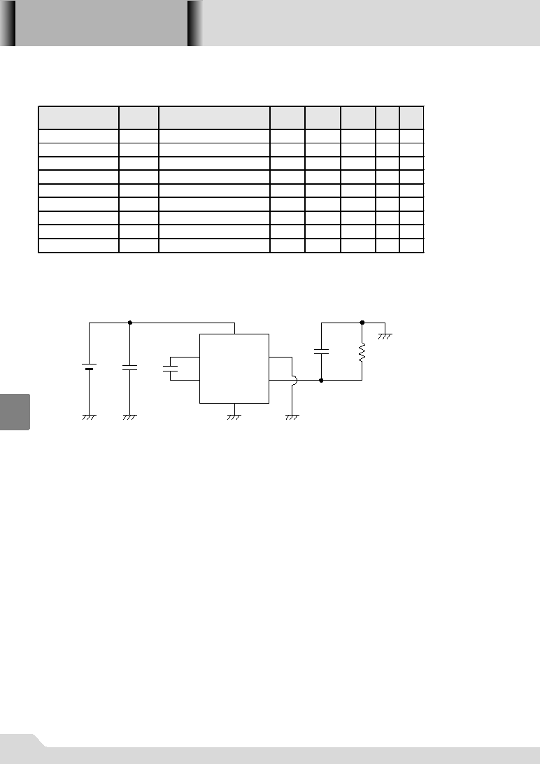
Typical Application Circuit
Typical Performance
Characteristic
+
C
IN
V
IN
+
C1
V
OUT
GND
CE/
V
DD
C+
C-
+
C2
R
L
0
20
40
60
80
100
0
2
4
6
8
10
XC6351A120MR (120kHz)
C
IN
=1.0
µF(ceramic)
V
IN
=3.0V,C
1
=C
2
=1.0
µF(ceramic)
Output Current:I
OUT
(mA)
Efficiency:EFFI (%)
08S_02XC6351A 02.09.12 15:31 627

XC6351A
Series
628
8
Packaging Information
GSOT-26
Pin Configuration
Pin Assignment
Product Classification
GOrdering Information
5
6
4
2
1
3
GND
CE/
C1+
C1-
SOT-26
(TOP VIEW)
PIN NUMBER
SYMBOL
FUNCTION
GND
C1+
Reverse Output
Power Supply
C1-
External Capacitor +Pin
Chip Enable (Low Active)
V
OUT
V
IN
CE/
V
IN
V
OUT
External Capacitor -Pin
Ground
SYMBOL
120
Oscillation frequency 120kHz
Oscillation frequency 35kHz (custom)
035
M
R
Embossed Tape Standard feed
Embossed Tape Reverse feed
L
DESCRIPTION
Package SOT-26
qwert
qwe
r
t
0.95
0.5
1.9±0.2
2.9±0.2
1.1±0.1
00.1
0.15
0.2min
+0.1
-0.05
0.4
+0.1
-0.05
2.8±0.2
1.6
+0.2
-0.1
0.4
+0.1
-0.05
08S_02XC6351A 02.09.12 15:31 628

XC6351A
Series
629
8
Marking
1
2
3
4
SOT-26
(TOP VIEW)
DESIGNATOR
PRODUCTNAME
A
XC6351AM
q Represents the product series
w, e Represents the Oscillator frequency
0
DESIGNATOR
XC6351A035M
XC6351A120M
PRODUCT NAME
35kHz
120kHz
Oscillator
frequency
3
2
1
r Denotes the production lot number
0 to 9, A to Z repeated(G.I.J.O.Q.W excepted)
C1+
C1-
V
IN
CE/
Buffer
Oscillator
Chip
Enable
GND
P1
N2
N4
N3
V
OUT
1. In operation, the following conditions will be repeated alternately :
P1 & N3 ON : N2 & N4 OFF
P1 & N3 OFF : N2 & N4 ON
2. In standby mode, P1, N3 & N4 will be ON and N2 will be OFF.
The output pin V
OUT
will be connected to GND.
Note :
PARAMETER
SYMBOL
RATINGS
UNITS
V
IN
input voltage
V
IN
6
V
V
OUT
pin voltage
V
OUT
-6 0.3
V
C1+ pin voltage
C1+
-0.3 V
IN
+ 0.3
V
C1- pin voltage
C1-
V
OUT
- 0.3 0.3
V
CE/ pin voltage
CE/
-0.3 V
IN
+ 0.3
V
OUT pin current
I
OUT
50
mA
Continuous Total
Power Dissipation
Pd
150
mW
Ambient Operating Temperature
Topr
-30 80
°C
Storage Temperature
Tstg
-40 125
°C
Ta = 25
°C, GND = 0V
Block Diagram
Absolute Maximum Ratings
08S_02XC6351A 02.09.12 15:31 629
XC6351A
Series
630
8
FOSC120kHz
Ta25
°C
PARAMETER
SYMBOL
CONDITIONS
MIN
TYP
MAX
UNITS CIRCUIT
Supply Current
I
DD
310
520
µA
1
Operating Voltage Range
V
IN
R
L
5k
1.2
5.0
V
2
Oscillation Frequency
F
OSC
75
120
192
kHz
1
Power Transition Efficiency
EFFI
R
L
2k
90
%
2
Voltage Transition Efficiency
VEFFI
R
L
95
%
2
Output Impedence
R
OUT
R
L
5k
45
90
2
Stand -By Current
I
STB
CE/V
IN
2.0
µA
3
CE/ 'H' Level Voltage
V
CEH
0.9
V
3
CE/ 'L' Level Voltage
V
CEL
0.25
V
3
Measuring Conditions : Unless otherwise stated, V
IN
= 5.0V, CE/ = 0V
Electrical Characteristics
+
C
IN
V
IN
+
C1
V
OUT
GND
CE/
V
DD
C+
C-
+
C2
R
L
Peripherals :
C
IN
= 1
µF (ceramic capacitor)
C1 = C2 = 1
µF (ceramic capacitor)*
* With the custom 35kHz frequency, C1 = C2 = 3.3
µF
Please use the IC & peripherals within the specified electrical characteristic ranges and ensure that absolute maximum
ratings are not exceeded.
For C1 & C2, please use a capacitor with as small an ESR value as possible.
In order to reduce impedance between the IC's input pin and the power supply, we recommend that a capacitor (C
IN
)
be connected to the input side.
If an external power supply is applied to the output pin in order to have V
OUT
connected to GND during standby, large
current flows through the IC are a possibility.
Further, do not use a capacitor at C2 that has a large capacitance value.
Typical Application Circuit
GStandard Circuit
Directions for use
GNotes on Use
08S_02XC6351A 02.09.12 15:31 630

waveform
measurement
V
OUT
GND
CE/
V
DD
C+
C-
+
C
IN
V
IN
A
waveform
measurement
V
OUT
GND
CE/
V
DD
C+
C-
+
A
C
IN
V
IN
CE/
+
C
IN
V
IN
A
+
C1
V
OUT
GND
CE/
V
DD
C+
C-
+
C2
A
V
R
L
Circuit 1
Circuit 2
Circuit 3
Peripherals :
C
IN
= 1
µF (ceramic capacitor)
C
1
= C
2
= 1
µF (ceramic capacitor)*
* With the custom 35kHz frequency, C1 = C2 = 3.3
µF
Test Circuits
XC6351A
Series
631
8
08S_02XC6351A 02.09.12 15:31 631