PWM Controlled StepUp DC/DC Controllers/Converters
Series
437
4
General Description
Features
Applications
NCMOS Low Power Consumption
NOperating Voltage
: 0.9V~10.0V
NOutput Voltage Range
: 2.0V~7.0V
NOutput Voltage Accuracy: ±2.5%
NSelectable Oscillator Frequency
: 50kHz, 100kHz,
180kHz
The XC6371 series are a group of PWM controlled step-up DC/DC
converters.
On-chip proprietary phase compensation and soft start-up circuits ensure
excellent transient response and improved performance.
Output voltage can be selected from 2.0V to 7.0V in 0.1V increments
(accuracy: ±2.5%). Oscillator frequency is also selectable from three
frequencies; 50, 100, and 180kHz (accuracy: ±15%).
Every built-in switching transistor type enables a step-up circuit to be
configured using only three external components; a coil, a diode, and a
capacitor.
External transistor versions are available to accommodate high output
current applications.
5-pin packages, which are provided with either a CE (chip enable)
function that reduces power consumption during shut-down mode, or a
V
DD
pin (separated power and voltage detect pins) are available.
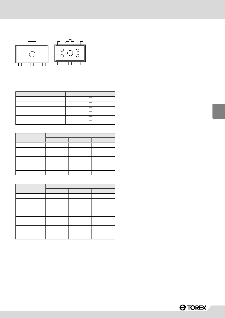
SOT-89 small package.
Operating (start-up) voltage range
: 0.9V~10V
Output voltage range : 2.0V~7.0V in 0.1V increments
Highly accurate
: Set-up voltage ±2.5%
Oscillator frequency
: 50kHz, 100kHz, 180khz (±15%)
selectable
Maximum output currents (Tr built-in)
: Typ.100mA @ V
IN
=3.0,
V
OUT
=5.0V .....Note(1)
Highly efficient (Tr built-in)
: Typ.85% @ V
IN
=3.0,
V
OUT
=5.0V .....Note(1)
Built-in switching transistor type and an external Tr type are
available.
Five-lead packaged units offer either Chip Enable or
independent V
OUT
pin option.
Phase compensation and soft start-up circuits built-in Small
package
: SOT-89 mini-power mold (3-pin, 5-pin)
Note(1): Performance depends on external components and
PCB layout.
GCellular phones, Pagers
GPalmtops
GCameras, Video recorders
GPortable products
Typical Application Circuit
Typical Performance
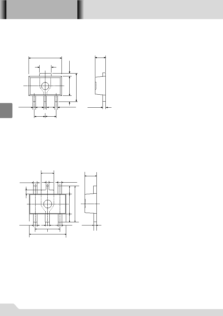
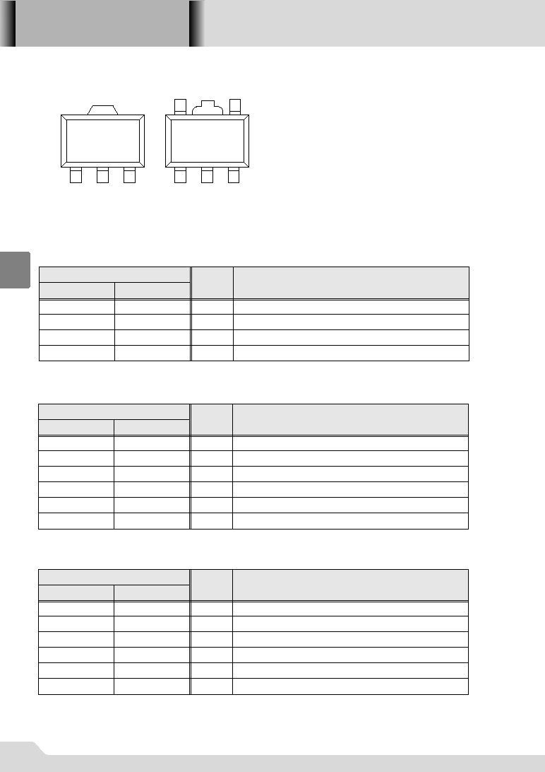
Characteristic
SOT-89
(TOP VIEW)
1
2
3
GND
V
OUT
C
L
Tantalum
L
SD
V
IN
C
IN
0.1
1
10
100
1000
L100HCR54
C
L
47FTantalum
Output Voltage:I
OUT
mA
XC6371A301PR
100
80
60
40
20
0
Efficiency:EFFI (%)
1.2V
1.5V
1.8V
2.7V
V
IN
=0.9V
04S_04XC6371 02.09.12 14:44 437
XC6371
Series
438
4
Pin Configuration
Pin Assignment
(XC6371A,XC6371B)
PIN NUMBER
XC6371A
XC6371B
PIN NAME
FUNCTION
1
1
V
SS
Ground
2
2
V
OUT
Output voltage monitor / IC internal power supply
3
Lx
Switch
3
EXT
External switch transistor drive
(XC6371C,XC6371D)
PIN NUMBER
XC6371C
XC6371D
PIN NAME
FUNCTION
5
5
V
SS
Ground
2
2
V
OUT
Output voltage monitor / IC internal power supply
4
Lx
Switch
4
EXT
External switch transistor drive
3
3
CE
Chip Enable
1
1
NC
No Connection
(XC6371E,XC6371F)
PIN NUMBER
XC6371E
XC6371F
PIN NAME
FUNCTION
5
5
V
SS
Ground
2
2
V
DD
IC internal power supply
4
Lx
Switch
4
EXT
External switch transistor drive
3
3
V
OUT
Output voltage monitor
1
1
NC
No Connection
SOT-89
(TOP VIEW)
1
2
3
SOT-89-5
(TOP VIEW)
1
2
3
4
5
04S_04XC6371 02.09.12 14:44 438
XC6371
Series
439
4
Product Classification
GSelection Guide
PART TYPE
PACKAGE
FEATURES
OPERATION
MODE
SWITCHING
RELATED
ADDITIONAL
FUNCTION
XC6371A
SOT-89
·
Switching transistor incorporated standard type.
·
Low ripple and highly efficient from low current
to high current.
Built-in Transistor
"Lx"lead
XC6371B
SOT-89
·
External switching transistor standard type.
·
Adding external transistor can improve the
output capability up to several hundred mA.
External Transistor
"EXT"lead
XC6371C
SOT-89-5
·
Stand-by (CE)function added version to the
XC6371A.
·
Stand-by current: 0.5
µA max.
Built-in Transistor
"Lx"lead
XC6371D
SOT-89-5
------------
------------
Chip Enable(CE)
Chip Enable(CE)
·
Stand-by (CE)function added version to the
XC6371B.
·
Stand-by current: 0.5
µA max.
External Transistor
"EXT"lead
XC6371E
SOT-89-5
·
Individual power supply and set-up voltage
sensing leads are available.
Built-in Transistor
"Lx"lead
Separated
"V
DD
"and"V
OUT
"leads
XC6371F
PWM
PWM
PWM
PWM
PWM
PWM
SOT-89-5
·
Individual power supply and set-up voltage
sensing leads are available.
External Transistor
"EXT"lead
Separated
"V
DD
"and"V
OUT
"leads
r
t
y
P
R
L
w
e
A
B
C
D
E
F
0
3-pin. Built-in switching transistor
3-pin. External switching transistor
Stand-by capability. Built-in switching transistor
Stand-by capability. External switching transistor
Separated V
DD
and V
OUT
. Built-in switching transistor
Separated V
DD
and V
OUT
. External switching transistor
OSC Frequency 50kHz
Output Voltage
e.g.,V
OUT
=3.5V
w=3, e=5
1
2
OSC Frequency 100kHz
OSC Frequency 180kHz
Embossed tape: Standard Feed
Embossed tape: Reverse Feed
Package q=A ~ B
SOT-89
q=C ~ F
SOT-89-5
XC6371 Series PWM Controlled
XC6371qwerty
q
GOrdering Information
04S_04XC6371 02.09.12 14:44 439
XC6371
Series
441
4
Marking
SOT-89
(TOP VIEW)
q
w
e
r
2
1
4
3
SOT-89-5
(TOP VIEW)
q Represents the Product Classification
XC6371F
DESIGNATOR
XC6371E
XC6371D
XC6371C
XC6371B
XC6371A
w Represents the integer of the Output Voltage and Oscillator Frequency
1
50
OSCILLATOR FREQUENCYkHz
INTEGER OF THE
OUTPUT VOLTAGE
B
180
1
100
1
5
4
3
2
r Denotes the production lot number
0 to 9, A to Z repeated(G.I.J.O.Q.W excepted)
PRODUCT NAME
C
2
2
D
3
3
E
4
4
F
5
5
6
H
6
6
7
K
7
7
A
B
A
B
S
X
e Represents the decimal number of the Output Voltage and Oscillator Frequency
0
9
50
OSCILLATOR FREQUENCYkHz
THE DECIMAL NUMBER OF
OUTPUT VOLTAGE
180
A
100
8
7
6
1
B
H
K
L
M
5
4
3
2
0
9
8
7
6
1
5
4
3
2
0
9
8
7
6
1
5
4
3
2
C
D
E
F
04S_04XC6371 02.09.12 14:44 441