PFM Controlled, StepUp DC/DC Converters (Duty Ratio 75%)
Series
487
4
General Description
Features
Applications
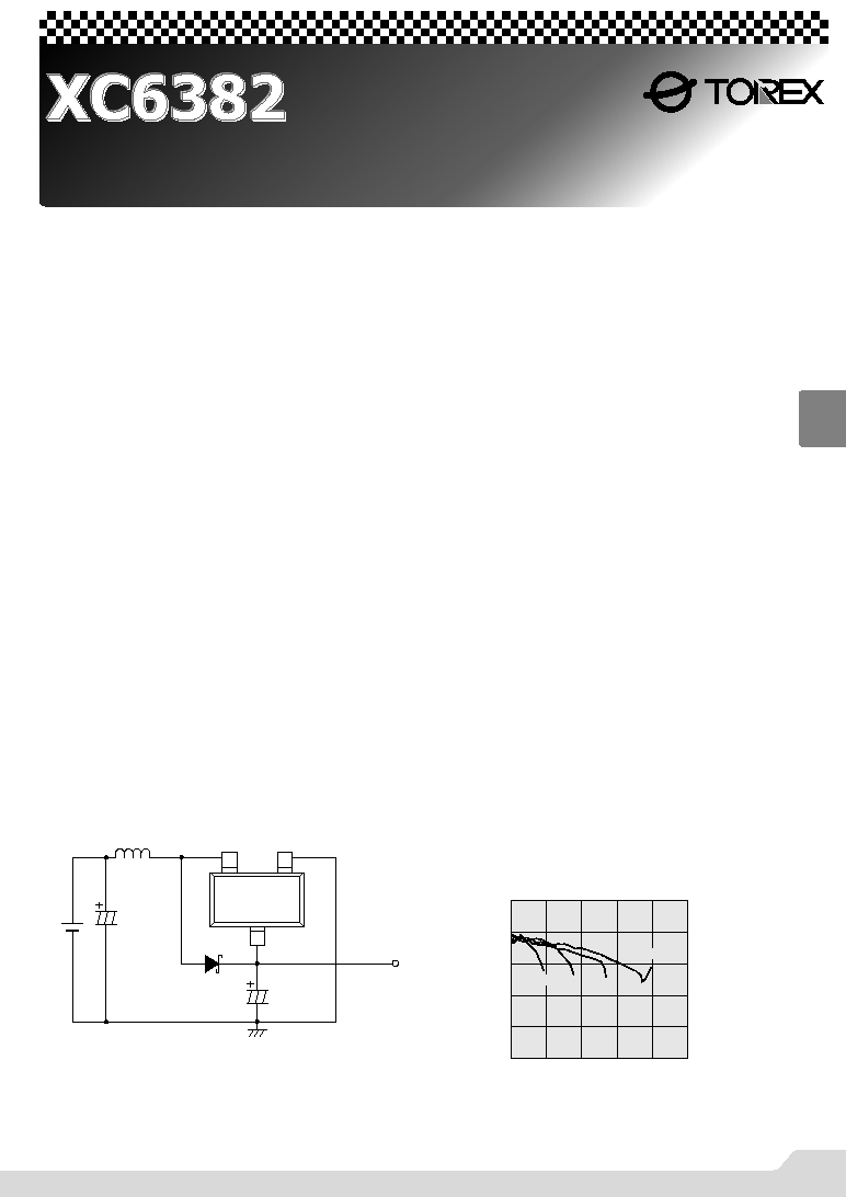
Typical Application Circuit
Typical Performance
Characteristic
NDuty 75%
NCMOS Low Power Consumption
NOperating Voltage
: 0.9V~10.0V
NOutput Voltage Range
: 2.0V~7.0V
NOutput Voltage Accuracy: ±2.5%
The XC6382 series is a group of PFM controlled step-up DC/DC
converters.
The XC6382 series employs CMOS process and laser trimming
technologies so as to attain low power and high accuracy.
Max. oscillator frequency is trimmed to 100kHz (accuracy: ±15%)
Every built-in switching transistor type enables a step-up circuit to be
configured using only three external components ; a coil, a diode, and a
capacitor.
External transistor versions are available to accommodate high output
current applications.
Both built-in and external transistor types include 5-pin and 3-pin
packages, which are provided with either a CE (chip enable) function that
reduces power consumption during shut-down mode, or a V
DD
pin
function (separating power and voltage detect pins).
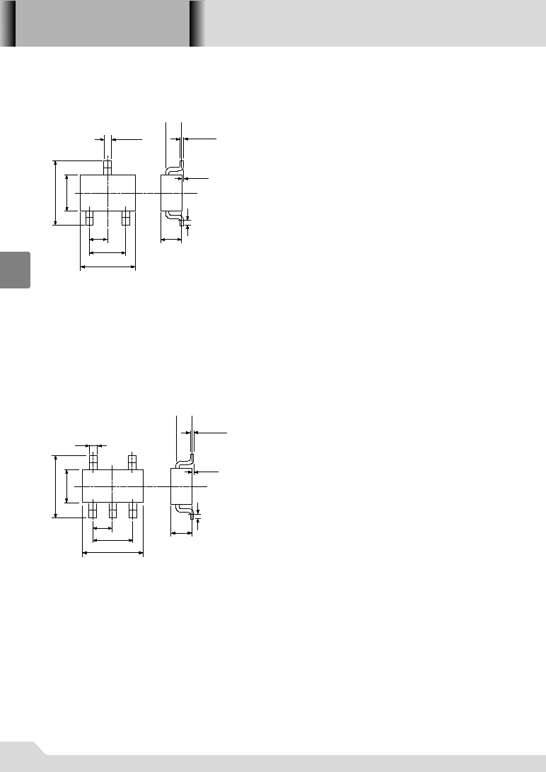
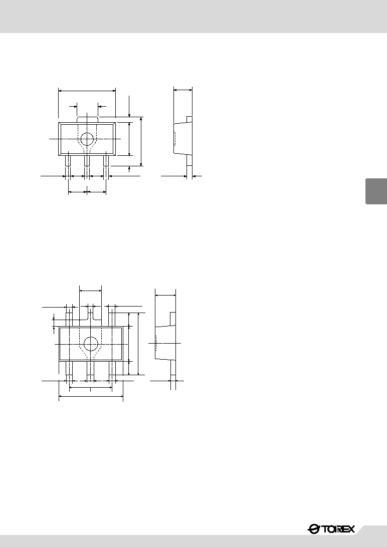
SOT-23, SOT-25 and SOT-89-5 super mini-mold packages.
Operating (start-up) voltage range
: 0.9V~10V
Output voltage range : 2.0V~7.0V in 0.1V increments
Highly accurate
: Set-up voltage ±2.5%
Maximum oscillator frequency
: 100kHz (±15%)
Duty ratio
: 75%(±5%)
Both switching transistor built-in and external types are
available.
Five-lead packaged units offer either Chip Enable or
independent V
OUT
pin option.
Small package
: SOT-23, 25 mini-mold (3-pin, 5-pin)
SOT-89, 89-5 mini-power mold
(3-pin, 5-pin)
GCellular phones, pagers
GPalmtops
GCameras, video recorders
GPortable equipment
2
1
(TOP VIEW)
SOT-23
3
V
OUT
SD
GND
C
L
Tantalum
L
V
IN
C
IN
XC6382A301
L=100H,C=47FTantalum
0
20
40
60
80
100
Output Current:I
OUT
mA
Efficiency:EFFI
100
80
60
40
20
0
1.5V
1.2V
0.9V
V
IN
=1.8V
04S_09XC6382 02.09.12 14:53 487
XC6382
Series
488
4
Pin Configuration
Pin Assignment
(XC6382A, XC6382B)
FUNCTION
Ground
Output voltage monitor, IC internal power supply
PIN NUMBER
Switch
XC6382A
SOT-23
SOT-89
SOT-23
SOT-89
PIN NAME
V
SS
V
OUT
Lx
1
1
1
1
3
2
3
2
2
3
XC6382B
EXT
2
3
External switch transistor drive
(XC6382C, XC6382D)
FUNCTION
Ground
Output voltage monitor, IC internal power supply
PIN NUMBER
Switch
XC6382C
SOT-25
SOT-89-5
SOT-25
SOT-89-5
PIN NAME
V
SS
V
DD
Lx
EXT
CE
NC
4
5
4
5
2
2
2
2
1
3
1
3
3
1
3
1
5
4
5
4
XC6382D
External switch transistor drive
Chip enable
No connection
(XC6382E, XC6382F)
FUNCTION
Ground
IC internal power supply
PIN NUMBER
Switch
XC6382E
SOT-25
SOT-89-5
SOT-25
SOT-89-5
PIN NAME
V
SS
V
DD
Lx
EXT
V
OUT
NC
4
5
4
5
2
2
2
2
1
3
1
3
3
1
3
1
5
4
5
4
XC6382F
External switch transistor drive
Output voltage monitor
No connection
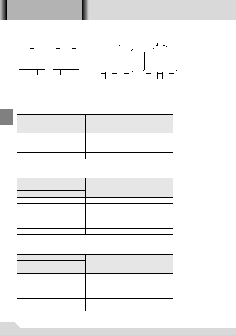
1
2
SOT-23
(TOP VIEW)
3
1
3
SOT-25
(TOP VIEW)
5
4
2
SOT-89
(TOP VIEW)
1
2
3
SOT-89-5
(TOP VIEW)
1
2
3
4
5
04S_09XC6382 02.09.12 14:53 488
XC6382
Series
489
4
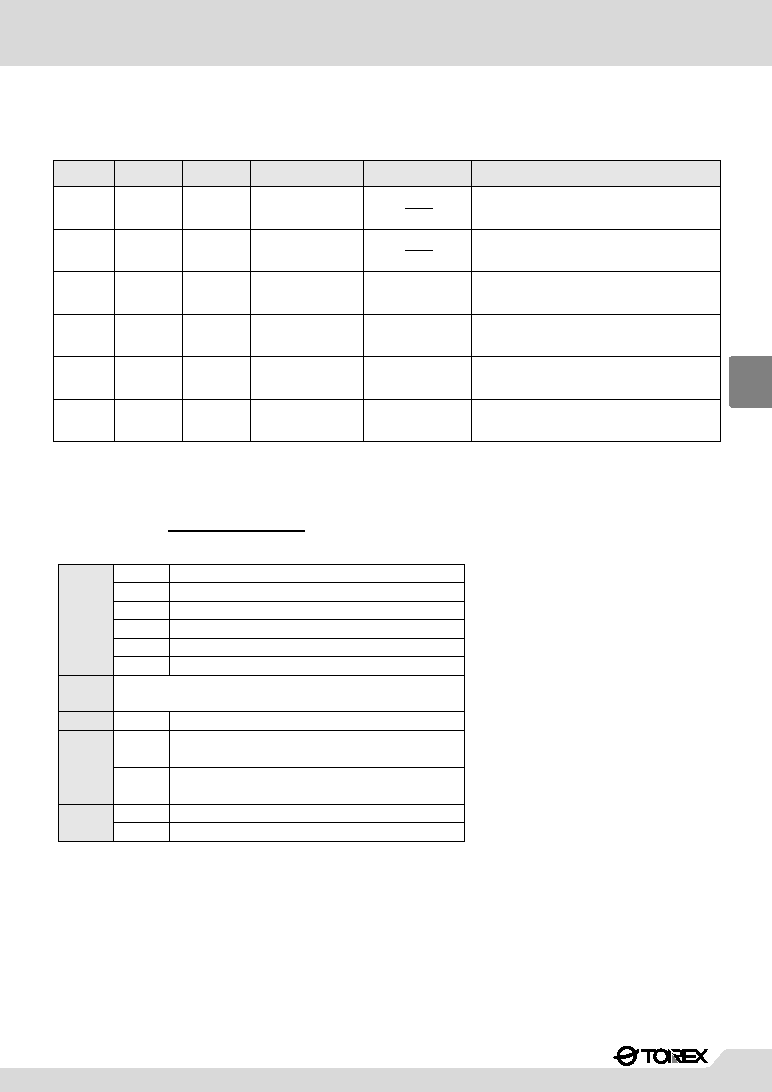
Product Classification
GSelection Guide
GOrdering Information
PART TYPE
PACKAGE
FEATURES
XC6382A
SOT-23,
SOT-89
SOT-23,
SOT-89
SOT-25,
SOT-89-5
SOT-25,
SOT-89-5
SOT-25,
SOT-89-5
SOT-25,
SOT-89-5
XC6382B
·
Accommodates a duty ratio of 75%.
·
Adding an external transistor can improve the output
capability by up to several hundred mA.
·
Accommodates a duty ratio of 75%.
XC6382C
·
Stand-by (CE) function added version to the
XC6382A.
·
Stand-by current: 0.5
µA max.
XC6382D
·
Stand-by (CE) function added version to the
XC6382B.
·
Stand-by current: 0.5
µA max.
XC6382E
·
Independent power supply and set-up voltage
sensing leads allow designing of PFM controllers.
XC6382F
·
Independent power supply and set-up voltage
sensing leads allow designing of PFM controllers.
ADDITIONAL
FUNCTION
Chip Enable(CE)
Chip Enable(CE)
Separated
"V
DD
" and "V
OUT
" leads
Separated
"V
DD
" and "V
OUT
" leads
DUTY
RATIO
75%
75%
75%
75%
75%
75%
SWITCHING
RELATED
Built-in Transistor
"Lx" lead
External Transistor
"EXT" lead
Built-in Transistor
"Lx" lead
External Transistor
"EXT" lead
Built-in Transistor
"Lx" lead
External Transistor
"EXT" lead
P
R
L
A
B
C
D
E
F
1
3-pin. Built-in switching transistor
3-pin. External switching transistor
Stand-by capability. (5-pin) Built-in switching transistor
Stand-by capability. (5-pin) External switching transistor
Separated V
DD
and V
OUT
. (5-pin) Built-in switching transistor
Separated V
DD
and V
OUT
. (5-pin) External switching transistor
Maximum Oscillator Frequency 100kHz
Output Voltage
e.g.V
OUT
=3.5V
w=3, e=5
M
Package
q=A~B
SOT-23
q=C~F
SOT-25
Package
q=A~B
SOT-89
q=C~F
SOT-89-5
Embossed tape : Standard Feed
Embossed tape : Reverse Feed
XC6382 Series
PFM Controlled Duty 75%
XC6382qwerty
q
w
e
r
t
y
04S_09XC6382 02.09.12 14:53 489