XC6401 Series
Dual LDO Regulators, Low ESR Cap. Compatible
November 7, 2003 Ver. 4
Preliminary
!
Low Power Consumption
: 25
µ
A (TYP)
!
APPLICATIONS
!
Dropout Voltage
: 30mV @ 30mA
"
Mobile phones (PDC, GSM, CDMA, IMT2000 etc.)
: 100mV @ 100mA
"
Cordless phones and radio communication equipment
!
Output Voltage Range
: 0.8 V to 5.0 V
"
Portable games
!
Output Current
: More than 150 mA (300mA limit)
"
Cameras, Video recorders
!
High Ripple Rejection Rate
: 70 dB @ 1kHz
"
Portable AV equipment
!
Low Output Noise
"
PDAs
!
Low ESR capacitor compatible
!
GENERAL DESCRIPTION
!
FEATURES
Maximum Output Current
: 150mA or more (300mA limit)
Dropout Voltage
: 100mV (IOUT=100mA)
Operating Voltage Range
: 1.5V ~ 6.0V
Output Voltage Range
: 0.8V ~ 5.0V (50mV Step)
Highly Accurate
: ±2% (VOUT>1.5V)
: ±30mV (VOUT
1.5V)
Low Power Consumption
: 25 mA (TYP.)
Standby Current
: Less than 0.1
µ
A (TYP.)
High Ripple Rejection
: 70dB (1kHz)
Operating Temperature Range
: -40
O
C ~ +85
O
C
Low ESR Capacitor Compatible
: Ceramic capacitor
Ultra Small Packages
: SOT-26W
USP-6B
!
TYPICAL APPLICATION CIRCUITS
!
TYPICAL PERFORMANCE CHARACTERISTICS
#
Cross Talk
V
IN
1
2
3
4
6
V
SS
V
OUT1
V
OUT2
EN1
EN2
5
C
IN
1uF
C
L2
1uF
C
L1
1uF
6
V
OUT2
V
OUT1
V
SS
EN2
V
IN
EN1
5
4
1
2
3
C
IN
1uF
C
L1
1uF
C
L2
1uF
The XC6401 series are highly accurate, Dual, low noise, CMOS LDO
voltage regulators. Performance features of the series includes low
output noise, high ripple rejection ratio, low dropout and very fast
turn-on times.
The XC6401 includes a reference voltage source, error amplifiers,
driver transistors, current limiters and phase compensators internally.
The XC6401's current limiters' foldback circuit also operates as a
short protect for the output current limiter.
The output voltage for each regulator is set independently by laser
trimming. Voltages are selectable in 50mV steps within a range of
0.8V to 5.0V. The XC6401 series is also fully compatible with low
ESR ceramic capacitors, reducing cost and improving output stability.
This high level of output stability is maintained even during frequent
load fluctuations, due to the excellent transient response
performance and high PSRR achieved across a broad range of
frequencies.
The EN function allows the output of each regulator to be turned off
independently, resulting in greatly reduced power consumption.
The XC6401 series is available in the SOT-26W or USP-6B `chip-
scale' package.
2.6
2.7
2.8
2.9
3.0
3.1
Time (40usec/div)
Output Voltage VOUT (V)
0
100
200
300
400
500
Output Current 1 IOUT (mA)
10mA
100mA
XC6401 (VR1:3.0V, VR2:2.85V)
VIN=4.0V, CIN= CL=1uF (ceramics)
VR1 Output Voltage (3.0V)
VR2 Output Voltage (2.85V)
VR1 Output Current
Semiconductor Ltd.
Data Sheet
1

XC6401 Series
Dual LDO Regulators, Low ESR Cap. Compatible
Preliminary
!
PIN CONFIGURATION
!
PIN ASSIGNMENT
*
A Pin number 1 is under the marking of the leftmost of 4 digits.
!
PRODUCT CLASSIFICATION
"
SELECTION GUIDE
The following options for the Regulator 1, 2, the EN pin logic, internal pull-up / down are available.
"
ORDERING INFORMATION
XC6401
123456
Regulator 1, EN type
Active 'High'
(Pull-down resistor built in)
Active 'High'
Regulator 1 Output Voltage Range :
(No pull-down, resistor built in)
0.8 ~ 5.0 V
Active 'Low'
Regulator 2 Output Voltage Range :
(Pull-down resistor built in)
0.8 ~ 5.0 V
Active 'Low'
Both 1 and 2 can be set 50 mV steps
(No pull-down, resistor built in)
Packaging Types
Regulator 2, EN type
Active 'High'
(Pull-down resistor built in)
Active 'High'
(No pull-down, resistor built in)
Device Orientation
Active 'Low'
(Pull-down resistor built in)
Active 'Low'
(No pull-down, resistor built in)
DESCRIPTION
34
01 ~
USP-6B
Internally set sequential number relating
output voltage of each regulators
SOT-26W
Embossed Tape: Standard Feed
Embossed Tape: Reverse Feed
DESCRIPTION
DESIGNATOR SYMBOL
5
D
M
6
DESIGNATOR SYMBOL
1
2
E
F
G
H
H
E
R
L
PIN NUMBER
PIN NAME
FUNCTION
ON/OFF Control 1
3
1
6
Power Input
ON/OFF Control 2
Output 2
4
USP-6B
3
2
SOT-26W
1
2
EN1
VIN
EN2
VOUT2
F
G
Ground
6
5
VOUT1
Output 1
4
VSS
5
SOT-26W
(TOP VIEW)
USP-6B
(TOP VIEW)
VOUT2
VOUT1
VSS
EN2
VIN
EN1
1
2
3
4
5
6
EN2
VIN
EN1
VSS
VOUT1
1
2
3
4
5
6
VOUT2
Semiconductor Ltd.
Data Sheet
2

XC6401 Series
Dual LDO Regulators, Low ESR Cap. Compatible
Preliminary
!
ABSOLUTE MAXIMUM RATINGS
Ta = 25
O
C
!
ELECTRICAL CHARACTERISTICS
XC6401FFxx
Regulator 1, Regulator 2
Ta=25
O
C
NOTE
(NOTE 1) VOUT(T)=Specified Output Voltage
(NOTE 2) VOUT(E)=Effective Output Voltage
(I.e. the output voltage when "VOUT(T)+1.0V" is provided at the VIN pin while maintaining a certain IOUT value).
(NOTE 3) Vdif={VIN1
(NOTE5)
-VOUT1
(NOTE4)
}
(NOTE 4) VOUT1=A voltage equal to 98% of the Output Voltage whenever an amply stabilized IOUT {VOUT(T)+1.0V} is input.
(NOTE 5) VIN1=The Input Voltage when VOUT1 appears as Input Voltage is gradually decreased.
(NOTE 6) Unless otherwise stated, VIN=VOUT(T)+1.0V
(NOTE 7)
If VOUT (T)
1.45V, MIN VOUT (T) - 30mV
MAX VOUT (T) + 30mV
µ
A
0.10
µ
A
V
0.25
V
4
4
VEN
VSS -0.3 ~ VIN +0.3
V
IOUT1 + IOUT2
VOUT
Supply Current
ISS
VIN=VEN=VOUT (T) + 1.0V,
IOUT=0mA
Output Voltage (Note 7)
VOUT (E)
Load Regulation
Dropout Voltage
VOUT
VIN=VOUT (T) + 1.0V
Ilim
Input Voltage
Temperature Characteristics
Topr
VOUT
VIN=VOUT (T) + 1.0V,
VEN=VSS
IOUT=30mA, f=1kHz
-40
O
C
Topr
85
O
C
EN "Low" Current
IENL
Storage Temperature
EN "High" Current
IENH
EN "Low" Voltage
VENL
Current Limiter
Short-circuit Current
Line Regulation
Vdif1
E-1
Operating Ambient Temperature
-55 ~ +125
CONDITIONS
Tstg
-40 ~ +85
Topr
IOUT=30mA
VIN=VOUT (T) + 1.0V
IOUT=30mA
VOUT /
IOUT=30mA
IOUT=100mA
6.0
0.20
VIN
VOUT
VOUT /
VIN
VOUT(T)+1.0V
VIN
6.0V
IOUT=30mA
25
45
0.01
◊
0.98
2
1
1.5
µ
A
V
% / V
E-2
60
MAX
V
TYP
VOUT(T)
◊
1.02
UNITS
Standby Current
ISTB
150
Maximum Output Current
IOUTMAX
1mA
IOUT
100mA
Vdif2
15
VIN=VEN=VOUT (T) + 1.0V, VEN=VSS
mA
1
4
0.10
VIN=VEN=VOUT (T) + 1.0V
VIN=VOUT (T) + 1.0V, VEN=VIN
30
-0.10
4
-0.10
300
1.60
Output Voltage
Ripple Rejection Rate
PSRR
EN "High" Voltage
VENH
Ishort
VIN=VOUT (T) + 1.0V, VEN=VIN
70
mV
mV
1
dB
5
mA
VIN
µ
A
1
±
100
1
3
ppm/
O
C
0.01
0.10
PARAMETER
SYMBOL
1
mV
mA
1
CIRCUIT
1
MIN
O
C
mW
O
C
EN Pin Voltage
Power Dissipation
SOT-26W
USP-6B
Pd
100
250
V
mA
700
VSS -0.3 ~ VIN +0.3
Output Current
Output Voltage
UNITS
PARAMETER
Input Voltage
RATINGS
V
6.5
VIN
SYMBOL
Semiconductor Ltd.
Data Sheet
3

XC6401 Series
Dual LDO Regulators, Low ESR Cap. Compatible
Preliminary
!
DROPOUT VOLTAGE
55
110
160
65
140
180
40
60
120
170
100
165
250
50
75
150
200
55
300
200
400
60
200
180
300
65
500
270
600
80
400
240
500
100
800
200
600
350
700
700
400
2.95
2.891
3.009
2.90
2.842
2.958
35
2.85
2.793
2.907
2.80
2.744
2.856
2.75
2.695
2.805
2.70
2.646
2.754
2.65
2.597
2.703
2.60
2.548
2.652
2.55
2.499
2.601
2.50
2.450
2.550
2.45
2.401
2.499
2.40
2.352
2.448
2.35
2.303
2.397
2.30
2.254
2.346
2.25
2.205
2.295
2.20
2.156
2.244
2.15
2.107
2.193
2.10
2.058
2.142
2.05
2.009
2.091
2.00
1.960
2.040
1.95
1.911
1.989
1.90
1.862
1.938
45
1.85
1.813
1.887
1.80
1.764
1.836
1.75
1.715
1.785
1.70
1.666
1.734
1.65
1.617
1.683
1.60
1.568
1.632
1.55
1.519
1.581
1.50
1.470
1.530
1.45
1.420
1.480
1.40
1.370
1.430
1.35
1.320
1.380
1.30
1.270
1.330
1.25
1.220
1.280
1.20
1.170
1.230
1.15
1.120
1.180
1.10
1.070
1.130
1.05
1.020
1.080
1.00
0.970
1.030
0.95
0.920
0.980
0.90
0.870
0.930
0.85
0.820
0.880
300
0.770
0.830
SETTING OUTPUT VOLTAGE
(V)
VOUT (T)
0.80
VOUT
Vdif 1
Vdif 2
OUTPUT VOLTAGE
(V)
DROPOUT VOLTAGE 1
E-1 (mV)
DROPOUT VOLTAGE 2
E-2 (mV)
MIN.
MAX.
MIN.
MAX.
MIN.
MAX.
Semiconductor Ltd.
Data Sheet
4

XC6401 Series
Dual LDO Regulators, Low ESR Cap. Compatible
Preliminary
!
DROPOUT VOLTAGE
30
4.95
4.851
5.049
5.00
4.900
5.100
4.85
4.753
4.947
4.90
4.802
4.998
4.845
4.80
4.704
4.896
150
4.65
4.557
4.743
4.70
4.606
4.794
4.55
4.75
4.655
4.459
4.641
4.60
4.508
4.692
4.45
4.361
4.539
4.50
4.410
4.590
4.35
4.263
4.437
4.40
4.312
4.488
4.25
4.165
4.335
4.30
4.214
4.386
4.15
4.067
4.233
4.20
4.116
4.284
4.05
3.969
4.131
4.10
4.018
4.182
3.95
3.871
4.029
4.00
3.920
4.080
3.85
3.773
3.927
3.90
3.822
3.978
3.75
3.675
3.825
3.80
3.724
3.876
3.65
3.577
3.723
3.70
3.626
3.774
3.55
3.479
3.621
3.60
3.528
3.672
3.45
3.381
3.519
3.50
3.430
3.570
3.35
3.283
3.417
3.40
3.332
3.468
3.25
3.185
3.315
3.30
3.234
3.366
3.15
3.087
3.213
3.20
3.136
3.264
3.05
2.989
3.111
3.10
3.038
3.162
MAX.
3.00
2.940
3.060
VOUT (T)
MIN.
MAX.
MIN.
45
100
SETTING OUTPUT VOLTAGE
OUTPUT VOLTAGE
DROPOUT VOLTAGE 1
DROPOUT VOLTAGE 2
(V)
E-1 (mV)
E-2 (mV)
(V)
VOUT
Vdif 1
Vdif 2
MAX.
MIN.
Semiconductor Ltd.
Data Sheet
5
XC6401 Series
Dual LDO Regulators, Low ESR Cap. Compatible
Preliminary
!
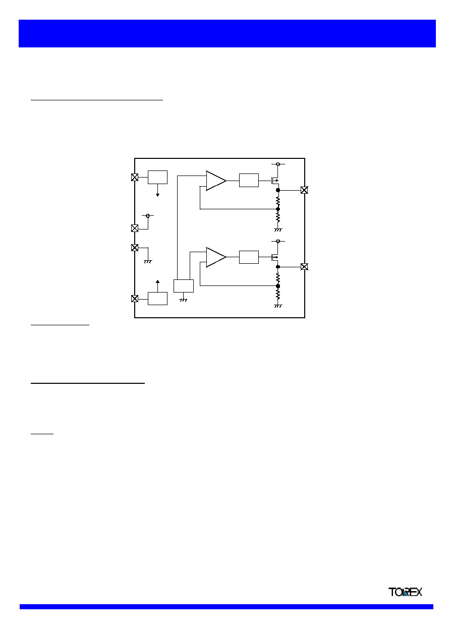
OPERATIONAL EXPLANATION
Output voltage control with the XC6401 series:
Low ESR Capacitors
Current Limiter, Short-Circuit Protection
EN Pins
!
NOTE ON USE
1
Please use this IC within the stated absolute maximum ratings.
The IC is liable to malfunction should the ratings be exceeded.
2
Where wiring impedance is high, operations may become unstable due to noise and/or phase lag
depending on output current. Please keep the resistance low between VIN and VSS wiring in particular.
3
Please wire the input capacitor (CIN) and the output capacitors (CL1, CL2) as close to the IC as possible.
The IC's internal circuitry can be shutdown via the signal from the EN1 and EN2 pins with the XC6401 series. In shutdown mode, output at the
VOUT1 and VOUT2 pins will be pulled down to the VSS level via R11 & R12 and R21 & R22. The operational logic of the IC's EN1 and EN2
pins are selectable (please refer to the selection guide on page 2). Note that as the standard XC6401FF type's regulator 1 and 2 are both ' High
Active/No Pull Down', operations will become unstable with the EN1 or EN2 pins open. Although the EN1 and EN2 pins are equal to an inverter
input with CMOS hysteresis, with either the pull-up or pull-down options, the EN1 and EN2 pins input current will increase when the IC is in
operation. We suggest that you use this IC with either a VIN voltage or a VSS voltage input at the EN1 and EN2 pins. If this IC is used with the
correct specifications for the EN1 and EN2 pins, the operational logic is fixed and the IC will operate normally. However, supply current may
increase as a result of through current in the IC's internal circuitry.
The voltage divided by resistors R1 & R2 is compared with the internal reference voltage by the error amplifier. The P-Channel MOSFETs,
which are connected to the VOUT1 and VOUT2 pins, are then driven by the subsequent output signal. The output voltages at the VOUT1 and
VOUT2 pins are controlled and stabilized by a system of negative feedback. The current limit circuit and short protect circuit operate in relation
to the level of output current. Further, the IC's internal circuitry can be shutdown via the EN pin's signal.
With the XC6401 series, a stable output voltage is achievable even if used with low ESR capacitors as a phase compensation circuit is built-in.
In order to ensure the effectiveness of the phase compensation, we suggest that output capacitors (CL1, CL2) is connected as close as
possible to the output pins (VOUT1 and VOUT2) and the VSS pin. Please use an output capacitor with a capacitance value of at least 1
µ
F. Also,
please connect an input capacitor (CIN) of 0.1
µ
F between the VIN pin and the VSS pin in order to ensure a stable power input.
The XC6401 series includes a combination of a fixed current limiter circuit & a foldback circuit which aid the operations of the current limiter and
circuit protection. When the load current reaches the current limit level, the fixed current limiter circuit operates and output voltage drops. As a
result of this drop in output voltage, the foldback circuit operates, output voltage drops further and output current decreases. When the output
pin is shorted, a current of about 30mA flows.
Current
Limit
Error
Amp1
ON/OFF
Control
VR1
Each
Circuit
VR2
Each
Circuit
Voltage
Reference
VOUT1
EN1
EN2
VIN
VSS
R11
R12
R21
R22
VOUT2
+
-
ON/OFF
Control
Current
Limit
+
-
Error
Amp2
Semiconductor Ltd.
Data Sheet
6
XC6401 Series
Dual LDO Regulators, Low ESR Cap. Compatible
Preliminary
!
TEST CIRCUITS
Circuit
1
EN1/EN2 :
Active 'High' = EN=VIN
Active 'Low' = EN=VSS
Circuit
2
EN1/EN2 :
1. Active 'High' (Pull-down resistor built-in)
VR1 Supply Current ISS1=I1 (Note:EN1=ON, EN2=OFF)
VR2 Supply Current ISS2=I1 (Note:EN1=OFF, EN2=ON)
2. Active 'High' (Pull-down, no resistor built-in)
VR1 Supply Current ISS1=I1 (Note:EN1=ON, EN2=OFF)
VR2 Supply Current ISS2=I1 (Note:EN1=OFF, EN2=ON)
3. Active 'Low' (Pull-up resistor built-in)
VR1 Supply Current ISS1=I1+I2 (Note:EN1=ON, EN2=OFF)
VR2 Supply Current ISS2=I1+I3 (Note:EN1=OFF, EN2=ON)
4. Active 'Low' (Pull-up, no resistor built-in)
VR1 Supply Current ISS1=I1 (Note:EN1=ON, EN2=OFF)
VR2 Supply Current ISS2=I1 (Note:EN1=OFF, EN2=ON)
Circuit
3
EN1/EN2 :
Active 'High' = EN=VSS
Active 'Low' = EN=VIN
V
I
OUT2
CIN, CL1, CL2 : 1
µ
F(ceramic)
CL2
CL1
V
I
OUT1
CIN
V
IN
V
OUT1
V
OUT2
EN1
V
SS
EN2
RL1
V
RL2
A
A
A
A
A
V
IN
I
OUT1
I
OUT2
V
IN
V
OUT1
V
OUT2
EN1
V
SS
EN2
A
A
I
3
I
2
I
1
CL2
CL1, CL2 :1
µ
F(ceramic)
CL1
A
V
IN
V
IN
V
OUT1
V
OUT2
EN1
V
SS
EN2
Semiconductor Ltd.
Data Sheet
7
XC6401 Series
Dual LDO Regulators, Low ESR Cap. Compatible
Preliminary
!
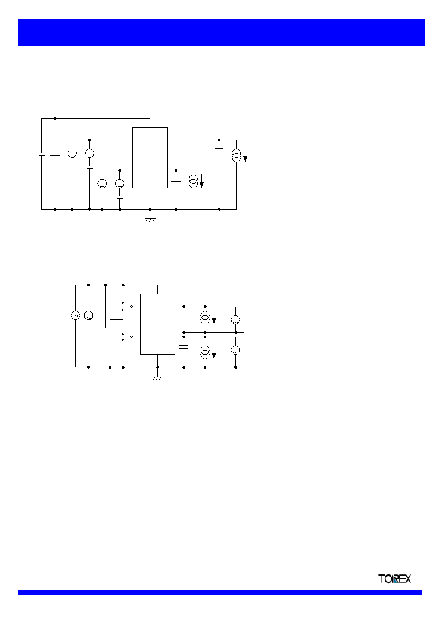
TEST CIRCUITS (Continued)
Circuit
4
Circuit
5
EN1/EN2 :
Active 'High' = EN=VIN
Active 'Low' = EN=VSS
V
IN
V
OUT1
V
OUT2
EN1
V
SS
EN2
A
V
A
V
VEN1
VEN2
CIN
CIN, CL1, CL2 :1
µ
F(ceramic )
I
OUT1
I
OUT2
CL2
CL1
I
OUT2
CL1, CL2 : 1
µ
F(ceramic)
CL2
CL1
I
OUT1
V
IN
=[V
OUT
(T)+1.0]
V+0.5Vp-pAC
V
IN
V
OUT1
V
OUT2
EN1
V
SS
EN2
V
V
V
Semiconductor Ltd.
Data Sheet
8

XC6401 Series
Dual LDO Regulators, Low ESR Cap. Compatible
Preliminary
!
TYPICAL PERFORMANCE CHARACTERISTICS
(1) Output Voltage vs. Output Current
0.0
0.5
1.0
1.5
2.0
2.5
3.0
3.5
4.0
0
50
100 150 200 250 300 350
Output Current IOUT (mA)
Output Voltage VOUT (V)
XC6401(2.85V)
0.0
0.5
1.0
1.5
2.0
2.5
3.0
3.5
4.0
0
50
100
150
200
250
300
350
Output Current IOUT (mA)
Output Voltage VOUT (V)
XC6401(2.85V)
0.0
0.5
1.0
1.5
2.0
2.5
3.0
3.5
4.0
0
50
100 150 200 250 300 350
Output Current IOUT (mA)
Output Voltage VOUT (V)
XC6401(3.0V)
0.0
0.2
0.4
0.6
0.8
1.0
0
50
100
150
200
250
300
350
Output Current IOUT (mA)
Output Voltage VOUT (V)
XC6401(0.8V)
0.0
0.2
0.4
0.6
0.8
1.0
0
50
100
150
200
250
300
350
Output Current IOUT (mA)
Output Voltage VOUT (V)
XC6401 (0.8V)
0.0
0.5
1.0
1.5
2.0
2.5
3.0
3.5
4.0
0
50
100 150 200 250 300 350
Output Current IOUT (mA)
Output Voltage VOUT (V)
XC6401(3.0V)
VIN=1.8V
CIN=1uF (ceramics), CL=1uF (ceramics)
Topr = 85
O
C
= 25
O
C
= - 40
O
C
VIN=4.0V
CIN=1uF (ceramics), CL=1uF (ceramics)
VIN = 6.0V
= 1.8V
= 1.8V
= 1.5V
VIN=4.0V
CIN=1uF (ceramics), CL=1uF (ceramics)
VIN = 6.0V
= 4.0V
= 3.15V
VIN=3.85V
CIN=1uF (ceramics), CL=1uF (ceramics)
Topr = 85
O
C
= 25
O
C
= - 40
O
C
VIN=4.0V
CIN=1uF (ceramics), CL=1uF (ceramics)
VIN = 6.0V
= 4.0V
= 3..3V
VIN=4.0V
CIN=1uF (ceramics), CL=1uF (ceramics)
Topr = 85
O
C
= 25
O
C
= - 40
O
C
Semiconductor Ltd.
Data Sheet
9

XC6401 Series
Dual LDO Regulators, Low ESR Cap. Compatible
Preliminary
(1) Output Voltage vs. Output Current (Continued)
(2) Output Voltage vs. Input Voltage
0.65
0.70
0.75
0.80
0.85
0.90
1.5 2.0 2.5 3.0 3.5 4.0 4.5 5.0 5.5 6.0
Input Voltage VIN (V)
Output Voltage VOUT (V)
XC6401(0.8V)
2.70
2.75
2.80
2.85
2.90
2.95
3.0
3.5
4.0
4.5
5.0
5.5
6.0
Input Voltage VIN (V)
Output Voltage VOUT (V)
XC6401(2.85V)
2.05
2.25
2.45
2.65
2.85
3.05
2.35
2.85
3.35
Input Voltage VIN (V)
Output Voltage VOUT (V)
XC6401(2.85V)
0.0
1.0
2.0
3.0
4.0
5.0
6.0
0
50
100
150
200
250
300
350
Output Current IOUT (mA)
Output Voltage VOUT (V)
XC6401(5.0V)
0.0
1.0
2.0
3.0
4.0
5.0
6.0
0
50
100 150 200 250 300 350
Output Current IOUT (mA)
Output Voltage VOUT (V)
XC6401(5.0V)
0.5
0.6
0.7
0.8
0.9
1.0
1.1
1.2
0.5
1.0
1.5
2.0
2.5
Input Voltage VIN (V)
Output Voltage VOUT (V)
XC6401(0.8V)
VIN=6.0V
CIN=1uF (ceramics), CL=1uF (ceramics)
Topr = 85
O
C
= 25
O
C
= - 40
O
C
VIN = 6.0V
= 5.3V
VIN=4.0V
CIN=1uF (ceramics), CL=1uF (ceramics)
Topr = 25
O
C
CIN=1uF (ceramics), CL=1uF (ceramics)
IOUT = 0mA
= 30mA
= 100mA
Topr = 25
O
C
CIN=1uF (ceramics), CL=1uF (ceramics)
IOUT = 0mA
= 30mA
= 100mA
Topr = 25
O
C
CIN=1uF (ceramics), CL=1uF (ceramics)
IOUT = 0mA
= 30mA
= 100mA
Topr = 25
O
C
CIN=1uF (ceramics), CL=1uF (ceramics)
IOUT = 0mA
= 30mA
= 100mA
Semiconductor Ltd.
Data Sheet
10
XC6401 Series
Dual LDO Regulators, Low ESR Cap. Compatible
Preliminary
(2) Output Voltage vs. Input Voltage (Continued)
(3) Dropout Voltage vs. Output Current
4.85
4.90
4.95
5.00
5.05
5.10
5.5
6.0
Input Voltage VIN (V)
Output Voltage VOUT (V)
XC6401(5.0V)
2.85
2.90
2.95
3.00
3.05
3.10
3.5
4.0
4.5
5.0
5.5
6.0
Input Voltage VIN (V)
Output Voltage VOUT (V)
XC6401(3.0V)
0.0
0.1
0.2
0.3
0.4
0.5
0
50
100
150
200
Output Current IOUT (mA)
Dropout Voltage Vdif (V)
XC6401(2.85V)
2.2
2.4
2.6
2.8
3.0
3.2
2.5
3.0
3.5
Input Voltage VIN (V)
Output Voltage VOUT (V)
XC6401(3.0V)
4.2
4.4
4.6
4.8
5.0
5.2
4.5
5.0
5.5
Input Voltage VIN (V)
Output Voltage VOUT (V)
XC6401(5.0V)
0.0
0.2
0.4
0.6
0.8
1.0
0
50
100
150
200
Output Current IOUT (mA)
Dropout Voltage Vdif (V)
XC6401(0.8V)
Topr = 25
O
C
CIN=1uF (ceramics), CL=1uF (ceramics)
IOUT = 0mA
= 30mA
= 100mA
Topr = 25
O
C
CIN=1uF (ceramics), CL=1uF (ceramics)
IOUT = 0mA
= 30mA
= 100mA
IOUT = 0mA
= 30mA
= 100mA
Topr = 25
O
C
CIN=1uF (ceramics), CL=1uF (ceramics)
IOUT = 0mA
= 30mA
= 100mA
CIN=1uF (ceramics), CL=1uF (ceramics)
Topr = 85
O
C
= 25
O
C
= - 40
O
C
CIN=1uF (ceramics), CL=1uF (ceramics)
Topr = 85
O
C
= 25
O
C
= - 40
O
C
Semiconductor Ltd.
Data Sheet
11

XC6401 Series
Dual LDO Regulators, Low ESR Cap. Compatible
Preliminary
(3) Dropout Voltage vs. Output Current (Continued)
0
20
40
60
80
100
0
1
2
3
4
5
6
Intput Voltage VIN (V)
Supply Current ISS (uA)
XC6401(2.85V)
0
20
40
60
80
100
0
1
2
3
4
5
6
Input Voltage VIN (V)
Supply Current ISS (uA)
XC6401(5.0V)
0
20
40
60
80
100
0
1
2
3
4
5
6
Input Voltage VIN (V)
Supply Current ISS (uA)
XC6401(3.0V)
0
20
40
60
80
100
0
1
2
3
4
5
6
Input Voltage VIN (V)
Supply Current ISS (uA)
XC6401(0.8V)
0.0
0.1
0.2
0.3
0.4
0.5
0
50
100
150
200
Output Current IOUT (mA)
Dropout Voltage Vdif (V)
XC6401(3.0V)
0.0
0.1
0.2
0.3
0.4
0.5
0
50
100
150
200
Output Current IOUT (mA)
Dropout Voltage Vdif (V)
XC6401(5.0V)
CIN=1uF (ceramics), CL=1uF (ceramics)
Topr = 85
O
C
= 25
O
C
= - 40
O
C
CIN=1uF (ceramics), CL=1uF (ceramics)
Topr = 85
O
C
= 25
O
C
= - 40
O
C
Topr = 85
O
C
= 25
O
C
= - 40
O
C
Topr = 85
O
C
= 25
O
C
= - 40
O
C
Topr = 85
O
C
= 25
O
C
= - 40
O
C
Topr = 85
O
C
= 25
O
C
= - 40
O
C
Semiconductor Ltd.
Data Sheet
12

XC6401 Series
Dual LDO Regulators, Low ESR Cap. Compatible
Preliminary
(5) Output Voltage vs. Ambient Temperature
(6) Supply Current vs. Ambient Temperature
20
22
24
26
28
30
-50
-25
0
25
50
75
100
Ambient Temperature Topr (
O
C)
Output Voltage VOUT (V)
XC6401(2.85V)
2.75
2.80
2.85
2.90
2.95
-50
-25
0
25
50
75
100
Ambient Temperature Topr (
O
C)
Output Voltage VOUT (V)
XC6401(2.85V)
20
22
24
26
28
30
-50
-25
0
25
50
75
100
Ambient Temperature Topr (
O
C)
Output Voltage VOUT (V)
XC6401(0.8V)
4.80
4.90
5.00
5.10
5.20
-50
-25
0
25
50
75
100
Ambient Temperature Topr (
O
C)
Output Voltage VOUT (V)
XC6401(5.0V)
2.90
2.95
3.00
3.05
3.10
-50
-25
0
25
50
75
100
Ambient Temperature Topr (
O
C)
Output Voltage VOUT (V)
XC6401(3.0V)
0.76
0.78
0.80
0.82
0.84
-50
-25
0
25
50
75
100
Ambient Temperature Topr (
O
C)
Output Voltage VOUT (V)
XC6401(0.8V)
VIN = 3.85V
VIN = 4.0V
CIN=1uF (ceramics), CL=1uF (ceramics)
IOUT = 0mA
= 10mA
= 30mA
= 100mA
VIN = 1.8V
CIN=1uF (ceramics), CL=1uF (ceramics)
IOUT = 0mA
= 10mA
= 30mA
= 100mA
VIN = 5.0V
CIN=1uF (ceramics), CL=1uF (ceramics)
IOUT = 0mA
= 10mA
= 30mA
= 100mA
VIN = 4.0V
CIN=1uF (ceramics), CL=1uF (ceramics)
IOUT = 0mA
= 10mA
= 30mA
= 100mA
VIN = 1.8V
Semiconductor Ltd.
Data Sheet
13

XC6401 Series
Dual LDO Regulators, Low ESR Cap. Compatible
Preliminary
(6) Supply Current vs. Ambient Temperature (Continued)
20
22
24
26
28
30
-50
-25
0
25
50
75
100
Ambient Temperature Topr (
O
C)
Output Voltage VOUT (V)
XC6401(5.0V)
20
22
24
26
28
30
-50
-25
0
25
50
75
100
Ambient Temperature Topr (
O
C)
Output Voltage VOUT (V)
XC6401(3.0V)
VIN = 4.0V
VIN = 6.0V
Semiconductor Ltd.
Data Sheet
14
XC6401 Series
Dual LDO Regulators, Low ESR Cap. Compatible
Preliminary
(7) Input Transient Response
2.75
2.80
2.85
2.90
2.95
3.00
3.05
Time (40usec/div)
Output Voltage VOUT (V)
0
1
2
3
4
5
6
Input Voltage VIN (V)
XC6401(2.85V)
2.75
2.80
2.85
2.90
2.95
3.00
3.05
Time (40usec/div)
Output Voltage VOUT (V)
0
1
2
3
4
5
6
Input Voltage VIN (V)
XC6401(2.85V)
2.75
2.80
2.85
2.90
2.95
3.00
3.05
Time (200usec/div)
Output Voltage VOUT (V)
0
1
2
3
4
5
6
Input Voltage VIN (V)
XC6401(2.85V)
0.70
0.75
0.80
0.85
0.90
0.95
1.00
Time (40usec/div)
Output Voltage VOUT (V)
-2
-1
0
1
2
3
4
Input Voltage VIN (V)
XC6401(0.8V)
0.70
0.75
0.80
0.85
0.90
0.95
1.00
Time (40usec/div)
Output Voltage VOUT (V)
-2
-1
0
1
2
3
4
Input Voltage VIN (V)
XC6401(0.8V)
0.70
0.75
0.80
0.85
0.90
0.95
1.00
Time (200usec/div)
Output Voltage VOUT (V)
-2
-1
0
1
2
3
4
Input Voltage VIN (V)
XC6401(0.8V)
tr=tf=5use
CL=1uF (ceramics), IOUT=100uA
Input Voltage
Output Voltage
tr=tf=5use
CL=1uF (ceramics), IOUT=30mA
Output Voltage
Input Voltage
tr=tf=5use
CL=1uF (ceramics), IOUT=100mA
Input Voltage
Output Voltage
tr=tf=5use
CL=1uF (ceramics), IOUT=100uA
Input Voltage
Output Voltage
tr=tf=5use
CL=1uF (ceramics), IOUT=100mA
tr=tf=5use
CL=1uF (ceramics), IOUT=30mA
Output Voltage
Input Voltage
Input Voltage
Output Voltage
Semiconductor Ltd.
Data Sheet
15

XC6401 Series
Dual LDO Regulators, Low ESR Cap. Compatible
Preliminary
(7) Input Transient Response (Continued)
4.90
4.95
5.00
5.05
5.10
5.15
5.20
Time (40usec/div)
Output Voltage VOUT (V)
2
3
4
5
6
7
8
Input Voltage VIN (V)
XC6401(5.0V)
4.90
4.95
5.00
5.05
5.10
5.15
5.20
Time (40usec/div)
Output Voltage VOUT (V)
2
3
4
5
6
7
8
Input Voltage VIN (V)
XC6401(5.0V)
4.90
4.95
5.00
5.05
5.10
5.15
5.20
Time (200usec/div)
Output Voltage VOUT (V)
2
3
4
5
6
7
8
Input Voltage VIN (V)
XC6401(5.0V)
2.90
2.95
3.00
3.05
3.10
3.15
3.20
Time (40usec/div)
Output Voltage VOUT (V)
0
1
2
3
4
5
6
Input Voltage VIN (V)
XC6401(3.0V)
2.90
2.95
3.00
3.05
3.10
3.15
3.20
Time (40usec/div)
Input Voltage VIN (V)
0
1
2
3
4
5
6
Input Voltage VIN (V)
XC6401(3.0V)
2.90
2.95
3.00
3.05
3.10
3.15
3.20
Time (200usec/div)
Output Voltage VOUT (V)
0
1
2
3
4
5
6
Input Voltage VIN (V)
XC6401(3.0V)
tr=tf=5use
CL=1uF (ceramics), IOUT=100uA
Input Voltage
Output Voltage
tr=tf=5use
CL=1uF (ceramics), IOUT=30mA
Input Voltage
Output Voltage
tr=tf=5use
CL=1uF (ceramics), IOUT=100uA
tr=tf=5use
CL=1uF (ceramics), IOUT=100mA
Output Voltage
Output Voltage
Input Voltage
Input Voltage
tr=tf=5use
CL=1uF (ceramics), IOUT=30mA
tr=tf=5use
CL=1uF (ceramics), IOUT=100mA
Input Voltage
Input Voltage
Output Voltage
Output Voltage
Semiconductor Ltd.
Data Sheet
16

XC6401 Series
Dual LDO Regulators, Low ESR Cap. Compatible
Preliminary
(8) Load Transient Response
2.45
2.55
2.65
2.75
2.85
2.95
Time (40usec/div)
Output Voltage VOUT (V)
0
50
100
150
200
250
Output Current IOUT (mA)
10mA
100mA
XC6401(2.85V)
2.45
2.55
2.65
2.75
2.85
2.95
Time (40usec/div)
Output Voltage VOUT (V)
0
50
100
150
200
250
Output Current IOUT (mA)
10mA
50mA
XC6401(2.85V)
2.60
2.70
2.80
2.90
3.00
3.10
Time (40usec/div)
Output Voltage VOUT (V)
0
50
100
150
200
250
Output Current IOUT (mA)
10mA
100mA
XC6401(3.0V)
2.60
2.70
2.80
2.90
3.00
3.10
Time (40usec/div)
Output Voltage VOUT (V)
0
50
100
150
200
250
Output Current IOUT (mA)
10mA
50mA
XC6401(3.0V)
0.40
0.50
0.60
0.70
0.80
0.90
Time (40usec/div)
Output Voltage VOUT (V)
0
50
100
150
200
250
Output Current IOUT (mA)
10mA
100mA
XC6401(0.8V)
0.40
0.50
0.60
0.70
0.80
0.90
Time (40usec/div)
Output Voltage VOUT (V)
0
50
100
150
200
250
Output Current IOUT (mA)
10mA
50mA
XC6401(0.8V)
VIN=1.8V, tr=tf=5use
CIN=CL=1uF (ceramics)
Output Current
Output Voltage
VIN=1.8V, tr=tf=5use
CIN=CL=1uF (ceramics)
Output Voltage
Output Current
VIN=4.0V, tr=tf=5use
CIN=CL=1uF (ceramics)
VIN=4.0V, tr=tf=5use
CIN=CL=1uF (ceramics)
Output Current
Output Voltage
Output Voltage
Output Current
VIN=4.0V, tr=tf=5use
CIN=CL=1uF (ceramics)
VIN=4.0V, tr=tf=5use
CIN=CL=1uF (ceramics)
Output Current
Output Voltage
Output Current
Output Voltage
Semiconductor Ltd.
Data Sheet
17

XC6401 Series
Dual LDO Regulators, Low ESR Cap. Compatible
Preliminary
(8) Load Transient Response (Continued)
4.60
4.70
4.80
4.90
5.00
5.10
Time (40usec/div)
Output Voltage VOUT (V)
0
50
100
150
200
250
Output Current IOUT (mA)
10mA
100mA
XC6401(5.0V)
4.60
4.70
4.80
4.90
5.00
5.10
Time (40usec/div)
Output Voltage VOUT (V)
0
50
100
150
200
250
Output Current IOUT (mA)
10mA
50mA
XC6401(5.0V)
VIN=6.0V, tr=tf=5use
CIN=CL=1uF (ceramics)
VIN=6.0V, tr=tf=5use
CIN=CL=1uF (ceramics)
Output Voltage
Output Voltage
Output Current
Output Current
Semiconductor Ltd.
Data Sheet
18

XC6401 Series
Dual LDO Regulators, Low ESR Cap. Compatible
Preliminary
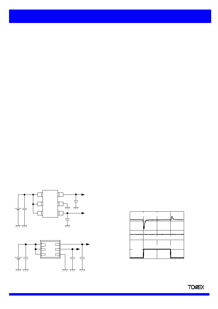
(9) Ripple Rejection Rate
(10) Cross Talk
2.6
2.7
2.8
2.9
3.0
3.1
Time (40usec/div)
Output Voltage VOUT (V)
0
100
200
300
400
500
Output Current 1 IOUT (mA)
10mA
100mA
XC6401 (VR1:3.0V, VR2:2.85V)
XC6401(5.0V)
0
20
40
60
80
0.01
0.1
1
10
100
Ripple Frequency f (kHz)
Ripple Rejection Rate RR (dB)
XC6401(3.0V)
0
20
40
60
80
0.01
0.1
1
10
100
Ripple Frequency f (kHz)
Ripple Rejection Rate RR (dB)
XC6401(0.8V)
0
20
40
60
80
0.01
0.1
1
10
100
Ripple Frequency f (kHz)
Ripple Rejection Rate RR (dB)
XC6401(2.85V)
0
20
40
60
80
0.01
0.1
1
10
100
Ripple Frequency f (kHz)
Ripple Rejection Rate RR (dB)
VIN=5.75V DC+0.5Vp-pAC
IOUT=30mA, CL=1uF (ceramics)
VIN=1.8V DC+0.5Vp-pAC
IOUT=30mA, CL=1uF (ceramics)
VIN=3.85V DC+0.5Vp-pAC
IOUT=30mA, CL=1uF (ceramics)
VIN=4.0V DC+0.5Vp-pAC
IOUT=30mA, CL=1uF (ceramics)
VIN=4.0V, CIN= CL=1uF (ceramics)
VR1 Output Voltage (3.0V)
VR2 Output Voltage (2.85V)
VR1 Output Current
Semiconductor Ltd.
Data Sheet
19