 | –≠–ª–µ–∫—Ç—Ä–æ–Ω–Ω—ã–π –∫–æ–º–ø–æ–Ω–µ–Ω—Ç: XC6402 | –°–∫–∞—á–∞—Ç—å:  PDF PDF  ZIP ZIP |
XC6402 Series
High Current, High Speed LDO Regulators, Voltage Detector Function
October 20, 2003 Ver. 2
!
Low Power Consumption
: 35
µ
A (TYP.)
!
APPLICATIONS
!
Maximum Output Current
: more than 700mA (800mA limit)
"
CD-ROM, CD-R / RW drive
!
Dropout Voltage
: 50mV @ 100mA
"
DVD drive
: 100mV @ 200mA
"
HDD drive
!
Operating Voltage Range
: 1.5V ~ 6.0V
"
Cameras, Video recorders
!
VR Output Voltage Range
: 0.8V ~ 5.0V
"
Portable AV equipment
VD Output Voltage Range
: 0.8V ~ 5.0V
"
Battery powered equipment
!
Low ESR capacitor compatible
!
GENERAL DESCRIPTION
!
FEATURES
Maximum Output Current
: more than 700mA (800mA limit)
(1.6V<VROUT(T)<5.0V)
Dropout Voltage
: 50mV @IOUT=100mA
Maximum Operating Voltage
: 1.5V ~ 6.0V
VR Output Voltage Range
: 0.8V ~ 5.0V (50mV step)
VD Output Voltage Range
: 0.8V ~ 5.0V (50mV step)
When monitoring VIN : more than 1.5V
Highly Accurate
: ± 2%
Low Power Consumption
: 35
µ
A (TYP.)
High Ripple Rejection
: 60dB (@1kHz)
Operational Ambient Temperature:
: - 40 ~ 85
O
C
Low ESR Capacitor Compatible
: Ceramic capacitor
Ultra Small Packages
: SOT-25 (SOT-23-5)
: SOT-89-5
: USP-6B
* VD: Voltage Detector
!
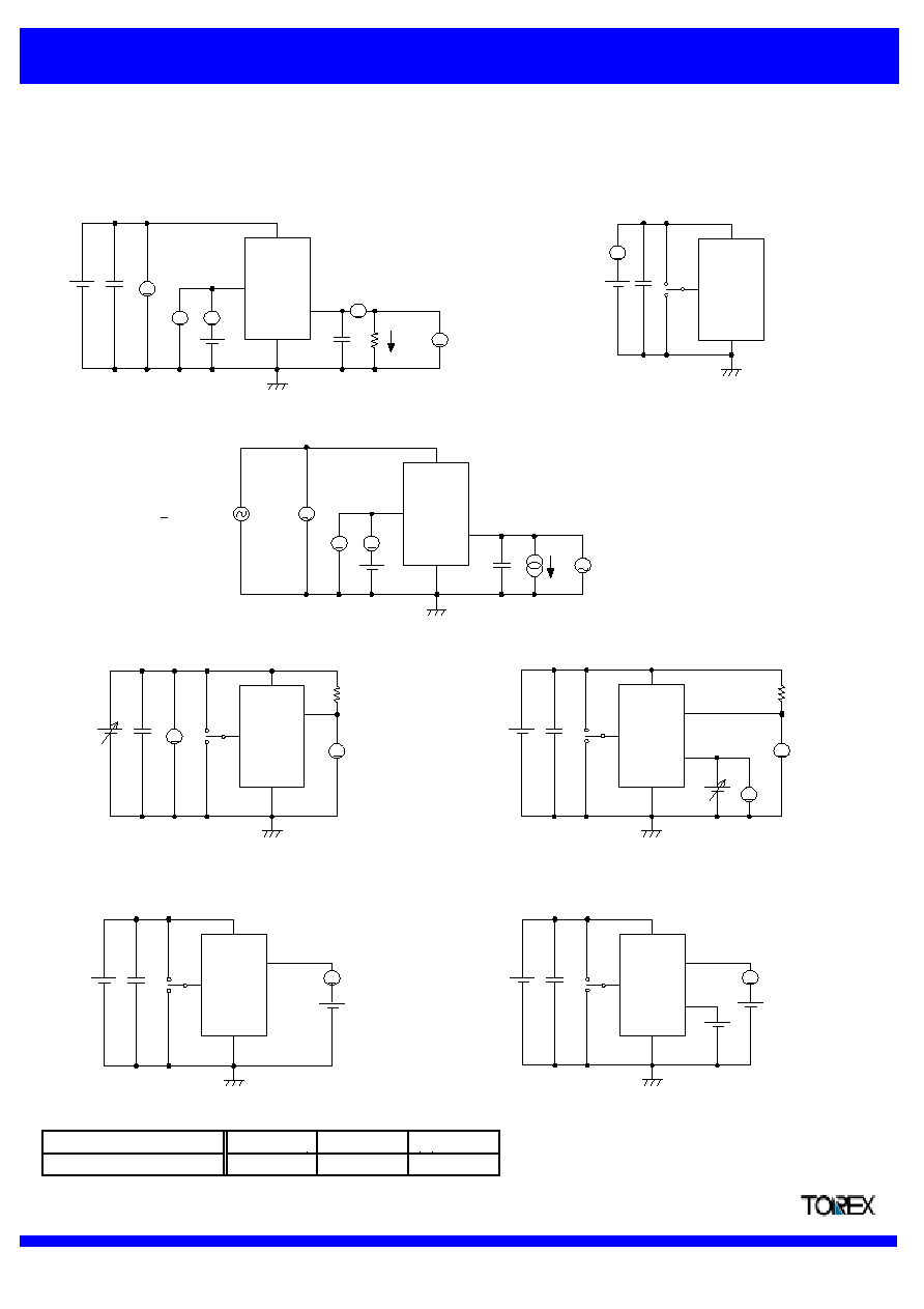
TYPICAL APPLICATIONS CIRCUITS
!
TYPICAL PERFORMANCE CHARACTERISTICS
#
XC6402C Series
#
Dropout Voltage vs. VR Output Current
#
XC6402F Series
The XC6402 series are precise, low noise, high current, positive voltage
low dropout regulators with built-in voltage detector. They are fabricated
using Torex's CMOS process. The series features a voltage reference,
an error amplifier, a current limiter, a voltage detector and a phase
compensation circuit plus a driver transistor.
The output voltage of the LDO and detect voltage of the detector is
selectable in 50mV increments within the range of 0.8V to 5.0V.
With a low ON resistance driver transistor built-in, batteries can be used
until input-output voltage differential is minimal and can accordingly be
used for a longer time.
The series is also compatible with low ESR ceramic capacitors which
give added output stability.
The series provides options to the user to select from a variety of circuit
features, such as detector monitoring, detector output logic, EN pin input
logic, and internal pull-up / down resistance (semi-custom).
The IC's internal regulator circuit can be placed in stand-by mode via the
EN function (XC6402C series). In the stand-by mode, power
consumption is greatly reduced.
The XC6402F series offers the option of a delay on the detector output:
the delay time can be controlled by the use of an external capacitor.
Semiconductor Ltd.
V
SS
1
3
4
5
VR
OUT
VD
OUT
V
IN
EN
220K
2
Rpull-up
CL
1uF
CIN
1uF
V
SS
1
3
4
5
VR
OUT
VD
OUT
V
IN
EN
220K
2
Rpull-up
CL
1uF
CIN
1uF
XC6402 Series (VR : 3.0V)
0.0
0.1
0.2
0.3
0.4
0.5
0.6
0.7
0.8
0.9
1.0
0
100
200
300
400
500
600
700
VR Output Current IROUT (mA)
D
r
op
out
V
o
l
t
a
ge V
d
i
f
(
V
)
CIN=1uF(ceramic), CL=1.0uF(ceramic)
- 40
O
C
- 25
O
C
- 85
O
C
Data Sheet
1

XC6402 Series
High Current, High Speed LDO Regulators, Voltage Detector Function
!
PIN CONFIGURATION
!
PIN ASSIGNMENT
!
SELECTION GUIDE
1. EN Input Logic, Internal Pull-up / down as option
* : C series
2. VD Sense as option
* : C and F series
3. VD Output Logic as option
* : C and F series
SOT-25
SOT-89-5
3
4
5
3
5
2
3
Active Low with pull-up resistance
VD Output
Detect H
VIN
XC6402 * A, B, E, F, L, M, R, S, V, X
VR Output
1
Delay Capacitor Connection ( F Series)
Cd
EN
XC6402 * A ~ D
VROUT
VDOUT
Active High with pull-down resistance
4
-
VR ON/OFF Control (C Series)
2
5
-
XC6402 * R ~ U
NC
Active Low with no pull-up resistance
VD SENSE PIN
XC6402 * E ~ K
Active High with no pull-down resistance
XC6402 * L ~ P
SERIES
CE INPUT LOGIC
SERIES
XC6402 * B, D, F, K, M, P, S, U, X, Z
Power Input
FUNCTION
VIN
VSS
PIN NAME
Ground
PIN NUMBER
5
6
1
USP-6B
3
4
1
2
1
No Connection
SERIES
VD OUTPUT LOGIC
XC6402 * A, C, E, H, L, N, R, T, V, Y
Detect L
XC6402 * C, D, H, K, N, P, T, U, Y, Z
VROUT
1
2
3
4
5
VR
OUT
VD
OUT
EN / Cd
V
IN
V
SS
SOT-25 (TOP VIEW)
SOT-89-5 (TOP VIEW)
USP-6B (TOP VIEW)
Semiconductor Ltd.
VIN
VSS
VROUT
VDOUT
EN / Cd
1
2
4
5
3
5
6
3
1
4
2
VDOUT
VROUT
VSS
EN / Cd
NC
VIN
Data Sheet
2

XC6402 Series
High Current, High Speed LDO Regulators, Voltage Detector Function
!
ORDERING INFORMATION
XC6402
123456
Denotes Optional Functions :
C : EN Function
M : SOT-25 (SOT-23-5)
P : SOT-89-5
D : USP-6B
Denotes Types :
Denotes Taping Direction:
As in the chart below.
R: Embossed tape, Standard feed
L : Embossed tape, Reverse feed
Detect Voltage Setting Range : 0.8V ~ 5.0V
50mV increments are available
PIN NUMBER :
2
Types
Denotes Packaging Types:
1
FUNCTION
PIN NUMBER
PIN NUMBER
FUNCTION
2
3 4
6
5
Internally set sequential number relating to output
voltage and detect voltage.
VR Setting Output Voltage Range : 0.8V ~ 5.0V
F : Cd Pin
E
F
H
A
B
C
D
M
N
P
K
L
U
V
X
R
S
T
Y
Z
EN FUNCTION
EN LOGIC
Functional
Functional
Functional
Functional
Functional
Functional
VD SENSE PIN
VD OUTPUT LOGIC
PULL UP/DOWN
RESISTANCE
PIN NUMBER
1
Functional
Functional
Functional
Functional
Functional
Functional
Functional
Functional
Functional
Functional
Nonfunctional
Nonfunctional
Nonfunctional
Nonfunctional
Active High
Pull-down Function
Active High
Pull-down Function
Active High
Nonfunctional
Active High
Nonfunctional
VIN
Detect L
Active High
Pull-down Function
VIN
Detect H
VROUT
Detect L
Active High
Pull-down Function
VROUT
Detect H
VIN
Detect L
Active High
Nonfunctional
VIN
Detect H
VROUT
Detect L
Active High
Nonfunctional
VROUT
Detect H
Active Low
Pull-up Function
VIN
Detect L
Active Low
Pull-up Function
VIN
Detect H
Active Low
Pull-up Function
VROUT
Detect L
VIN
Detect L
Active Low
Pull-up Function
VROUT
Detect H
C Series
Active Low
Nonfunctional
VROUT
Detect L
Active Low
Nonfunctional
VIN
Detect H
Active Low
Detect L
Active Low
Nonfunctional
VROUT
Detect H
Detect L
-
-
VIN
Detect H
Detect H
F Series
-
2
-
-
VROUT
-
VROUT
-
-
VIN
Nonfunctional
Semiconductor Ltd.
Data Sheet
3

XC6402 Series
High Current, High Speed LDO Regulators, Voltage Detector Function
!
PACKAGING INFORMATION
#
SOT-25 (SOT-23-5)
#
SOT-89-5
#
USP-6B
6
5
4
1
2
3
A'
A
AA
A
A
A
A
1
.
4
5
6
3
2
1
0
1
1
1
1
1
2.0 + 0.15
(0.45) 0.5+0.1
(0.05)
(0.45) (0.45)
45
O
45
O
1.8
+
0
.
15
(0.
2
7
)
(0
.2
7)
(0
.2
7)
(
0.
45
)
45
O
45
O
(0
.1
25
)
(0
.6
5)
0.
00
5+0
.
0
0
2
(0.
0
5
)
-0.00
5
+0
.
0
1
-0
.
0
5
+0
.
1
5
0.7+0.03
5-0
.
2
+
0.0
5
0
.
5+
0.
1
1.
6+0
.
1
5
0.
5+0
.
1
0.
1+
0
.
03
0.2
+
0
.
05
1.0+0.1
0.25+0.1
0.25+0.1
O
Semiconductor Ltd.
Data Sheet
4

XC6402 Series
High Current, High Speed LDO Regulators, Voltage Detector Function
!
BLOCK DIAGRAM
XC6402C Series
XC6402F Series
Optional:
Active HIGH with Pull-down R
Active HIGH with no Pull-down R
Active LOW with Pull-up R
Active LOW with no Pull-up R
EN
V
SS
VR
OUT
V
IN
R1
R2
R4
R3
VD
OUT
Comp. VD
Error Amp.
Optional:
Detect H
Detect L
C
FB
Optional:
V
IN
SENSE
VR
OUT
SENSE
Cd
V
SS
VR
OUT
V
IN
R2
R1
R4
R3
VD
OUT
Comp. VD
Error Amp.
Optional:
Detect H
Detect L
C
FB
Current
Limit
Voltage
Reference
Current
Limit
Optional:
V
IN
SENSE
VR
OUT
SENSE
ON / OFF
Control
Voltage
Reference
Rdelay
Semiconductor Ltd.
VR Circuit
Data Sheet
5
XC6402 Series
High Current, High Speed LDO Regulators, Voltage Detector Function
!
ABSOLUTE MAXIMUM RATINGS
Ta=25
O
C
!
ELECTRICAL CHARACTERISTICS
XC6402C Series
Ta=25
O
C
1
-
35
70
-
35
70
1
3
1
1
2
2
1
-
PARAMETER
SYMBOL
RATINGS
UNITS
Input Voltage
VIN
6.5
V
VR Output Current
IROUT
800
mA
VR Output Voltage
VROUT
VSS -0.3 ~ VIN +0.3
V
VD Output Current
IDOUT
50
mA
VD Output Voltage
VDOUT
VSS -0.3 ~ 6.5
V
VEN / Cd Pin Voltage
VEN / Cd
VSS -0.3 ~ VIN + 0.3
V
Continuous
Power Dissipation
SOT-25
Pd
250
mW
SOT-89-5
500
USP-6B
100
Operating Temperature Range
Topr
- 40 ~ + 85
O
C
Storage Temperature Range
Tstg
- 55 ~ + 125
O
C
UNITS
PARAMETER
SYMBOL
CONDITIONS
MIN
TYP
MAX
(-30mV)
(+30mV)
700
x 0.98
x 1.02
VROUT(T)
-
-
mA
-
-
mA
mV
1
1
500
VR Load Regulation
VROUT
-
Supply Current
(CA/CB/CC/CD type)
IDD
Vdif2
E-2 (page 8 ~9)
15
60
VR Dropout Voltage (note 4)
Supply Current
(CL/CM/CN/CP type)
IDD
VEN=VROUT(T)+1.0V, VIN=VSS,
IROUT=0mA
IROUT=30mA
IROUT=100mA
VEN=VIN=VROUT(T)+1.0V,
IROUT=0mA
Vdif1
E-1 (page 8 ~9)
VR Line Regulation
VROUT
-
VIN
VROUT
E-3 (page 8 ~9)
VEN=VIN=VROUT(T)+1.0V,
IROUT=0mA
E-3 (page 8 ~9)
-
6.0
V
0.01
0.20
% / V
Input Voltage
VIN
1.5
VROUT
-
Topr
VROUT
IROUT=30mA
-40
O
C<Topr<85
O
C
±
100
-
ppm /
O
C
VR Ripple Rejection Rate
PSRR
-
VIN=[VROUT(T)+1.0]VDC+0.5Vp-pAC
-
dB
VR Output Voltage
Temperature Characteristics
60
800
IROUT=30mA, f=1kHz
VIN=VROUT(T)+1.0V
VEN=ON(VIN or VSS)
When VROUT(T) > 4.75V
!
VIN=5.75V+0.5Vp-pAC
-
mA
VR Current Limiter
[VROUT(E)<1.6V]
IRlim
-
-
mA
VR Current Limiter
[VROUT(E)>1.6V]
IRlim
700
-
VIN=VROUT(T)+1.0V
VEN=ON(VIN or VSS)
VIN=VROUT(T)+1.0V
VEN=ON(VIN or VSS)
800
30
-
mA
V
VROUT(E)
1mA<IROUT<100mA
VR Output Voltage (note 2, 3)
VIN=VROUT(T)+1.0V, IROUT=30mA
VIN=VROUT(T)+1.0V
VEN=ON(VIN or VSS)
VIN=VROUT(T)+1.0V
VEN=ON(VIN or VSS)
VR Maximum Output Current
[VROUT(E)<1.6V]
IROUTMAX
VR Maximum Output Current
[VROUT(E)>1.6V]
IROUTMAX
1
2
2
µ
A
mV
µ
A
µ
A
µ
A
VEN=ON(VIN or VSS), IROUT=30mA
VROUT(T)+1.0V<VIN<6.0V
VEN=VROUT(T)+1.0V, VIN=VSS,
IROUT=0mA
VOLTAGE REGULATOR (VROUT=1.8V)
Supply Current
(CR/CS/CT/CU type)
IDD
Supply Current
(CE/CF/CH/CK type)
IDD
Short-Circuit Current
IRshort
CIRCUIT
1
1
Semiconductor Ltd.
Data Sheet
6
XC6402 Series
High Current, High Speed LDO Regulators, Voltage Detector Function
!
ELECTRICAL CHARACTERISTICS (Continued)
XC6402C Series
Ta=25
O
C
(NOTE 1) Unless otherwise stated, VIN=VROUT(T)+1.0V
(NOTE 2) VROUT(T)=Specified VR Output Voltage
(NOTE 4) Vdif={VIN1
(NOTE6)
-VROUT1
(NOTE5)
}
(NOTE 5) A voltage equal to 98% of the VR Output Voltage whenever a stabilized VROUT1=IROUT{VROUT(T)+1.0V} is input.
(NOTE 6) VIN1=The Input Voltage when VOUT1, which appears as Input Voltage is gradually decreased.
(NOTE 7) VDF (T) : Specified Detect Voltage value
(NOTE 8) VDF (E) : Actual Detect Voltage value.
(NOTE 9) VD Output Current value of Detect 'L' type equal to current value during detection
and that of Detect 'H' type equal to current value before detection.
(NOTE10) VROUT(T)<1.45V, VDF(T)<1.45V
!
MIN : VROUT(T) -30mV, VDF(T) -30mV,
!
MAX : VROUT(T) +30mV, VDF(T) +30mV
(NOTE11) EN conditions:
XC6402CA / CB / CC / CD / CE / CF / CH / CK type : ON=VIN, OFF=VSS
XC6402CL / CM / CN / CP / CR / CS / CT / CU type : ON=VSS, OFF=VIN
(NOTE12) VD detect voltage : For VIN Sense version, XC6402CA / CB / CE /CF / CL / CM / CR / CS, only VDF(T)>1.5V type are available.
1
1
1
1
5
4
1
1
CIRCUIT
4
4
2
x 1.02
VOLTAGE DETECTOR
VD Output Current
(note 9)
IDOUT
VD Detect Voltage (note 7, 8)
VDF (E)
V
x 0.02
VD Hysteresis Range (note 7)
VHYS
VDF (E)
VDF (E)
x 0.05
-
5.5
14.5
-
5.0
14.0
-
6.0
15.0
-
6.5
15.5
7.0
16.0
-
7.5
17.0
-
3.5
-
1.8
3.7
-
Topr
VDF
2.0
4.0
-
VDF /
-
VIN = 2.0V
1.8
ppm /
O
C
±
100
-
VIN = 6.0V
mA
1.9
3.8
PARAMETER
SYMBOL
UNITS
(+30mV)
V
CONDITIONS
MIN
TYP
MAX
x 0.08
VDF (E)
(-30mV)
VDF (T)
x 0.98
IDDVD
VD Supply Current
VIN = 2.0V
VIN = 3.0V
VIN = 4.0V
VIN = 5.0V
VIN = 6.0V
VEN = OFF (VIN or VSS)
VIN = 1.5V
µ
A
VDOUT = 0.5V
VIN = 1.5V
1.5
3.0
-
VIN = 3.0V
VIN = 4.0V
VIN = 5.0V
VIN
-
1.9
3.9
-
V
-40
O
C<Topr<85
O
C
EN "High" Level Voltage
VEN H
1.60
VD Detect Voltage
Temperature Characteristics
-
EN "High" Level Current
(CA/CB/CC/CD type)
IEN H
-0.10
-
EN "Low" Level Voltage
VEN L
-
VEN=VIN=VROUT(T)+1.0V
E-4
(page 8~9)
-
µ
A
0.25
V
EN "High" Level Current
(CE/CF/CH/CK/CL/CM/CN/
CP/CR/CS/CT/CU type)
IEN H
-0.10
EN "High" Level Current
(CL/CM/CN/CP type)
IEN L
VIN=VROUT(T)+1.0V, VEN=VSS
E-5
(page 8~9)
SWITCH
(NOTE 3) VROUT(E)=Actual VR Output Voltage.
(i.e. the VR output voltage when "VROUT(T)+1.0V" is provided at the VIN pin while maintaining a certain IROUT value).
-
0.10
µ
A
EN "High" Level Current
(CA/CB/CC/CD/CE/CF/CH/
CK/CR/CS/CT/CU type)
IEN L
VIN=VROUT(T)+1.0V, VEN=VSS
-0.10
µ
A
-
0.10
µ
A
-
0.10
Semiconductor Ltd.
Data Sheet
7

XC6402 Series
High Current, High Speed LDO Regulators, Voltage Detector Function
!
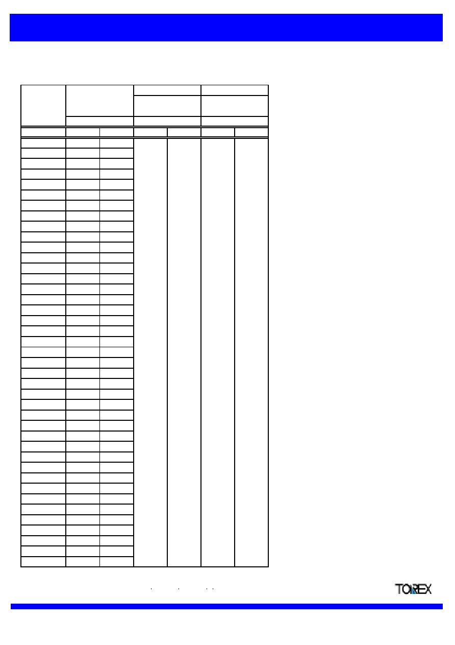
XC6402C SERIES DROPOUT VOLTAGE, SUPPLY CURRENT, EN'H/L' LEVEL CURRENT
VROUT(T)
MIN.
MAX.
TYP.
MAX.
VOUT
Vdif1
Vdif2
IDD
MAX.
TYP.
MAX.
TYP.
(V)
E-1
DROPOUT VOLTAGE 1
(mV)
VR OUTPUT VOLTAGE
VD DETECT VOLTAGE
(V)
SETTING
OUTPUT
VOLTAGE
E-2
E-3
DROPOUT VOLTAGE 2
SUPPLY CURRENT
(mV)
(
µ
A)
EN'H'LEVEL
CURRENT (
µ
A)
E-4
TYP.
E-5
EN'H'LEVEL
CURRENT (
µ
A)
IENL
MAX.
IENH
0.80
0.770
0.830
0.85
0.820
0.880
0.90
0.870
0.930
0.95
0.920
0.980
1.00
0.970
1.030
1.05
1.020
1.080
1.10
1.070
1.130
1.15
1.120
1.180
1.20
1.170
1.230
1.25
1.220
1.280
1.30
1.270
1.330
1.35
1.320
1.380
1.40
1.370
1.430
1.45
1.420
1.480
1.50
1.470
1.530
1.55
1.519
1.581
1.60
1.568
1.632
1.65
1.617
1.683
1.70
1.666
1.734
1.75
1.715
1.785
1.80
1.764
1.836
1.85
1.813
1.887
1.90
1.862
1.938
1.95
1.911
1.989
2.00
1.960
2.040
2.05
2.009
2.091
2.10
2.058
2.142
2.15
2.107
2.193
2.20
2.156
2.244
2.25
2.205
2.295
2.30
2.254
2.346
2.35
2.303
2.397
2.40
2.352
2.448
2.45
2.401
2.499
2.50
2.450
2.550
2.55
2.499
2.601
2.60
2.548
2.652
2.65
2.597
2.703
2.70
2.646
2.754
2.75
2.695
2.805
2.80
2.85
2.90
2.95
2.744
2.856
2.793
2.907
2.842
2.958
2.891
3.009
100
700
600
250
5.0
-5.0
800
700
38.0
80.0
50
500
150
600
400
500
30
300
200
100
100
400
300
250
38.5
81.5
6.5
-6.5
27.0
41.0
90.0
135.0
39.0
83.0
8.0
-8.0
25.0
37.0
80.0
120.0
39.5
84.5
9.5
-9.5
18.0
28.0
60.0
90.0
40.0
86.0
11.0
-11.0
Semiconductor Ltd.
Data Sheet
8

XC6402 Series
High Current, High Speed LDO Regulators, Voltage Detector Function
!
XC6402C SERIES DROPOUT VOLTAGE, SUPPLY CURRENT, EN'H/L' LEVEL CURRENT (Continued)
SETTING
VR OUTPUT VOLTAGE
E-1
E-2
E-3
E-4
E-5
OUTPUT
VD DETECT VOLTAGE
DROPOUT VOLTAGE 1
DROPOUT VOLTAGE 2
SUPPLY CURRENT
EN'H'LEVEL
EN'H'LEVEL
VOLTAGE
(V)
(mV)
(mV)
(
µ
A)
CURRENT (
µ
A)
CURRENT (
µ
A)
(V)
VOUT
Vdif1
Vdif2
IDD
IENH
IENL
VROUT(T)
MIN.
MAX.
TYP.
MAX.
TYP.
MAX.
TYP.
MAX.
TYP.
MAX.
3.00
2.940
3.060
23.0
50.0
75.0
40.5
3.05
2.989
3.111
3.10
3.038
3.162
3.15
3.087
3.213
3.20
3.136
3.264
3.25
3.185
3.315
3.30
3.234
3.366
3.35
3.283
3.417
3.40
3.332
3.468
3.45
3.381
3.159
3.50
3.430
3.570
3.55
3.479
3.621
3.60
3.528
3.672
3.65
3.577
3.723
3.70
3.626
3.774
3.75
3.675
3.825
3.80
3.724
3.876
3.85
3.773
3.927
3.90
3.882
3.978
3.95
3.871
4.029
4.00
3.920
4.080
4.05
3.969
4.131
4.10
4.018
4.182
4.15
4.067
4.233
4.20
4.116
4.284
4.25
4.165
4.335
4.30
4.214
4.386
4.35
4.263
4.437
4.40
4.312
4.488
4.45
4.361
4.539
4.50
4.410
4.590
4.55
4.459
4.641
4.60
4.508
4.692
4.65
4.557
4.743
4.70
4.606
4.794
4.75
4.655
4.845
4.80
4.704
4.896
4.85
4.753
4.947
4.90
4.802
4.998
4.95
4.851
5.049
5.00
4.900
5.100
87.5
12.5
-12.5
15.0
41.0
89.0
14.0
-14.0
41.5
90.5
15.5
-15.5
42.0
92.0
17.0
-17.0
Semiconductor Ltd.
Data Sheet
9

XC6402 Series
High Current, High Speed LDO Regulators, Voltage Detector Function
!
ELECTRICAL CHARACTERISTICS
XC6402F Series
Ta=25
O
C
(NOTE 1) Unless otherwise stated, VIN=VROUT(T)+1.0V
(NOTE 2) VROUT(T)=Specified VR Output Voltage
(NOTE 4) Vdif={VIN1
(NOTE6)
-VROUT1
(NOTE5)
}
(NOTE 5) A voltage equal to 98% of the VR Output Voltage whenever a stabilized VROUT1=IROUT{VROUT(T)+1.0V} is input.
(NOTE 6) VIN1=The Input Voltage when VOUT1, which appears as Input Voltage is gradually decreased.
(NOTE 7) VDF (T) : Specified Detect Voltage value
(NOTE 8) VDF (E) : Actual Detect Voltage value.
(NOTE 9) VD Output Current value of Detect 'L' type equal to current value during detection
and that of Detect 'H' type equal to current value before detection.
(NOTE10) VROUT(T)<1.45V, VDF(T)<1.45V
!
MIN : VROUT(T) -30mV, VDF(T) -30mV,
!
MAX : VROUT(T) +30mV, VDF(T) +30mV
(NOTE11) VD detect voltage : For VIN Sense version, XC6402FV / FX, only VDF(T)>1.5V type are available.
±
100
-
ppm /
O
C
VD Detect Voltage
Temperature Characteristics
VDF /
-40
O
C<Topr<85
O
C
-
Topr
VDF
4
4
5
6
4
2.0
3.5
M
Delay Resistance
Rdelay
VIN=6.0V, Vcd=0V
1.0
(i.e. the VR output voltage when "VROUT(T)+1.0V" is provided at the VIN pin while maintaining a certain IROUT value).
(NOTE 3) VROUT(E)=Actual VR Output Voltage.
VIN = 6.0V
-
2.0
4.0
VD Output Current
(note 9)
IDOUT
VDOUT=0.5V
-
1.9
3.8
VIN = 5.0V
-
1.9
3.9
µ
A
1.5
3.0
1.8
3.5
1.8
3.7
-
VDF (E)
VDF (E)
VIN = 1.5V
-
VIN = 2.0V
-
V
x 0.05
x 0.08
VD Hysteresis Range (note 7)
VHYS
VDF (E)
x 0.02
V
(-30mV)
(+30mV)
1
1
1
x 0.98
VDF (T)
x 1.02
30
VOLTAGE DETECTOR
VD Detect Voltage (note 7, 8)
VDF (E)
VIN = 3.0V
VIN = 4.0V
1
1
3
-
1
1
1
-
35
70
2
µ
A
E-2 (page 11~12)
15
-
mA
Short-Circuit Current
IRshort
VIN=VROUT(T)+1.0V
-
800
-
mA
VR Current Limiter
[VROUT(E)<1.6V]
IRlim
VIN=VROUT(T)+1.0V
-
800
-
mA
VR Current Limiter
[VROUT(E)>1.6V]
IRlim
VIN=VROUT(T)+1.0V
700
VR Ripple Rejection Rate
PSRR
VIN=[VROUT(T)+1.0]VDC+0.5Vp-pAC
-
When VROUT(T) > 4.75V
!
VIN=5.75V+0.5Vp-pAC
IROUT=30mA, f=1kHz
60
-
dB
-
6.0
V
±
100
-
ppm /
O
C
VR Output Voltage
Temperature Characteristics
VROUT
IROUT=30mA
-
Topr
VROUT
-40
O
C<Topr<85
O
C
Input Voltage
VIN
1.5
0.01
0.20
% / V
VR Line Regulation
VROUT
VROUT(T)+1.0V<VIN<6.0V
-
VIN
VROUT
IROUT=30mA
Supply Current
IDD
VIN=VROUT(T)+1.0V
Vdif2
IROUT=100mA
60
mV
VR Dropout Voltage (note 4)
Vdif1
IROUT=30mA
E-1 (page 11~12)
mV
VR Load Regulation
VROUT
1mA<IROUT<100mA
-
mA
1
VR Maximum Output Current
[VROUT(E)<1.6V]
IROUTMAX
VIN=VROUT(T)+1.0V
500
-
-
mA
(-30mV)
(+30mV)
VR Maximum Output Current
[VROUT(E)>1.6V]
IROUTMAX
VIN=VROUT(T)+1.0V
700
-
-
CIRCUIT
VOLTAGE REGULATOR
VR Output Voltage (note 2, 3)
VROUT(E)
VIN=VROUT(T)+1.0V, IROUT=30mA
x 0.98
VROUT(T)
x 1.02
V
1
MIN
TYP
MAX
UNITS
PARAMETER
SYMBOL
CONDITIONS
Semiconductor Ltd.
Data Sheet
10
XC6402 Series
High Current, High Speed LDO Regulators, Voltage Detector Function
!
XC6402F SERIES DROPOUT VOLTAGE
2.95
2.891
3.009
2.85
2.793
2.907
2.90
2.842
2.958
2.75
2.695
2.805
2.80
2.744
2.856
2.65
2.597
2.703
2.70
2.646
2.754
2.55
2.499
2.601
2.60
2.548
2.652
18.0
28.0
60.0
90.0
2.45
2.401
2.499
2.50
2.450
2.550
2.35
2.303
2.397
2.40
2.352
2.448
2.25
2.205
2.295
2.30
2.254
2.346
2.15
2.107
2.193
2.20
2.156
2.244
2.05
2.009
2.091
2.10
2.058
2.142
25.0
37.0
80.0
120.0
1.95
1.911
1.989
2.00
1.960
2.040
1.85
1.813
1.887
1.90
1.862
1.938
1.715
1.785
1.80
1.764
1.836
41.0
90.0
135.0
1.55
1.519
1.581
1.60
1.568
1.632
1.65
1.50
1.470
1.530
27.0
1.617
1.683
1.70
1.666
1.734
1.75
100
250
1.45
1.420
1.480
300
1.35
1.320
1.380
300
100
400
1.25
1.220
1.280
1.30
1.270
1.330
200
1.20
1.170
1.230
30
1.40
1.370
1.430
500
1.15
1.120
1.180
500
150
600
1.05
1.020
1.080
1.10
1.070
1.130
400
1.00
0.970
1.030
50
600
700
0.95
0.920
0.980
0.85
0.820
0.880
0.90
0.870
0.930
MAX.
TYP.
MAX.
0.80
0.770
0.830
100
700
250
800
VROUT(T)
MIN.
MAX.
TYP.
(V)
VOUT
Vdif1
Vdif2
VOLTAGE
(V)
(mV)
(mV)
OUTPUT
VD DETECT VOLTAGE
DROPOUT VOLTAGE 1
DROPOUT VOLTAGE 2
SETTING
VR OUTPUT VOLTAGE
E-1
E-2
Semiconductor Ltd.
Data Sheet
11
XC6402 Series
High Current, High Speed LDO Regulators, Voltage Detector Function
!
XC6402F SERIES DROPOUT VOLTAGE (Continued)
4.95
4.851
5.049
5.00
4.900
5.100
4.85
4.753
4.947
4.90
4.802
4.998
4.75
4.655
4.845
4.80
4.704
4.896
4.65
4.557
4.743
4.70
4.606
4.794
4.55
4.459
4.641
4.60
4.508
4.692
4.45
4.361
4.539
4.50
4.410
4.590
4.35
4.263
4.437
4.40
4.312
4.488
4.25
4.165
4.335
4.30
4.214
4.386
4.15
4.067
4.233
4.20
4.116
4.284
4.05
3.969
4.131
4.10
4.018
4.182
3.95
3.871
4.029
4.00
3.920
4.080
3.85
3.773
3.927
3.90
3.882
3.978
3.75
3.675
3.825
3.80
3.724
3.876
3.65
3.577
3.723
3.70
3.626
3.774
3.55
3.479
3.621
3.60
3.528
3.672
3.45
3.381
3.159
3.50
3.430
3.570
3.35
3.283
3.417
3.40
3.332
3.468
3.25
3.185
3.315
3.30
3.234
3.366
3.15
3.087
3.213
3.20
3.136
3.264
3.05
2.989
3.111
3.10
3.038
3.162
MAX.
TYP.
MAX.
3.00
2.940
3.060
15.0
23.0
50.0
75.0
VROUT(T)
MIN.
MAX.
TYP.
(V)
VOUT
Vdif1
Vdif2
VOLTAGE
(V)
(mV)
(mV)
E-1
E-2
OUTPUT
VD DETECT VOLTAGE
DROPOUT VOLTAGE 1
DROPOUT VOLTAGE 2
SETTING
VR OUTPUT VOLTAGE
Semiconductor Ltd.
Data Sheet
12
XC6402 Series
High Current, High Speed LDO Regulators, Voltage Detector Function
!
TEST CIRCUITS
XC6402C Series
#
Circuit
1
#
Circuit
2
#
Circuit
3
#
Circuit
4
XC6402CA / CB / CE / CF/ CL / CM / CS type
XC6402 CC / CD / CH / CK / CN / CP / CT / CU type
#
Circuit
5
XC6402CA / CB / CE / CF/ CL / CM / CS type
XC6402 CC / CD / CH / CK / CN / CP / CT / CU type
Output Capacitor Corresponding Chart
CL
6.8
µ
F
2.2
µ
F
1.0
µ
F
VR OUTPUT VOLTAGE
0.8 ~1.45V
1.5 ~ 1.75V
1.8V ~ 5.0V
Semiconductor Ltd.
V
A
V
V
IN
CIN
CIN: 1uF (ceramic)
VRI
OUT
CL
VEN
V
IN
VD
OUT
VR
OUT
EN
V
SS
V
A
V
A
CL
VEN
V
IN
VD
OUT
VR
OUT
EN
V
SS
V
V
VIN={VROUT+1.0V}VDC+0.5Vp-pAC
VROUT>4.75V
VIN=5.75VDC+0.5Vp-pAC
V
V
IN
VD
OUT
VR
OUT
EN
V
SS
100k
V
V
IN
CIN
CIN: 1uF (ceramic)
V
V
IN
VD
OUT
VR
OUT
EN
V
SS
100k
V
V
IN
CIN
CIN: 1uF (ceramic)
V
IN
VD
OUT
VR
OUT
EN
V
SS
A
VDS
CIN
CIN: 1uF (ceramic)
V
IN
VD
OUT
VR
OUT
EN
V
SS
A
CIN
VDS
CIN:1 uF (ceramic)
CIN
A
V
IN
VD
OUT
VR
OUT
EN
V
SS
CIN:1uF (ceramic)
.
Data Sheet
13

XC6402 Series
High Current, High Speed LDO Regulators, Voltage Detector Function
!
TEST CIRCUITS (Continued)
XC6402F Series
#
Circuit
1
#
Circuit
2
#
Circuit
3
#
Circuit
4
XC6402FV / FX type
XC6402FY / FZ type
#
Circuit
5
XC6402FV / FX type
XC6402FY / FZ type
#
Circuit
6
XC6402FV / FX type
XC6402FY / FZ type
Output Capacitor Corresponding Chart
VR OUTPUT VOLTAGE
0.8 ~1.45V
CL
6.8
µ
F
1.5 ~ 1.75V
2.2
µ
F
1.8V ~ 5.0V
1.0
µ
F
Semiconductor Ltd.
V
V
IN
CIN
CIN: 1uF (ceramic)
VRI
OUT
CL
V
IN
VD
OUT
VR
OUT
Cd
V
SS
V
A
A
V
IN
VD
OUT
VR
OUT
Cd
V
SS
CIN
CIN: 1uF (ceramic)
.
CL
V
V
VIN={VROUT+1.0V}VDC+0.5Vp-pAC
VROUT>4.75V
VIN=5.75VDC+0.5Vp-pAC
V
IN
VD
OUT
VR
OUT
Cd
V
SS
V
100k
V
V
IN
CIN
V
IN
VD
OUT
VR
OUT
Cd
V
SS
CIN: 1uF (ceramic)
V
100k
V
V
IN
CIN
V
IN
VD
OUT
VR
OUT
Cd
V
SS
CIN: 1uF (ceramic)
A
VDS
CIN
V
IN
VD
OUT
VR
OUT
Cd
V
SS
CIN: 1uF (ceramic)
A
CIN
VDS
V
IN
VD
OUT
VR
OUT
Cd
V
SS
CIN: 1uF (ceramic)
V
IN
VD
OUT
VR
OUT
Cd
V
SS
A
CIN
.
V
IN
VD
OUT
VR
OUT
Cd
V
SS
A
CIN
.
Data Sheet
14

XC6402 Series
High Current, High Speed LDO Regulators, Voltage Detector Function
!
OPERATIONAL EXPLANATION
<Output voltage regulator control>
<Detector function with the XC6402 series>
Delay Time
Rdelay standard : 1.0 ~ 3.5M
TYP : 2.0M
<Low ESR Capacitors>
Output Capacitor Corresponding Chart
<Current Limiter, Short-Circuit Protection>
0.8 ~1.45V
6.8
µ
F
1.5 ~ 1.75V
2.2
µ
F
1.8V ~ 5.0V
1.0
µ
F
Delay Time = Cdelay x Rdelay x 0.7
The voltage, divided by resistors R1 & R2 which are connected to the VROUT pin is compared with the internal reference voltage by the error amplifier. The
P-Channel MOSFET, which is connected to the VROUT pin, is then driven by the subsequent output signal. The output voltage at the VROUT pin is controlled
& stabilized by negative feedback. The
current limit circuit and short circuit protection operate in relation to the level of output current. Further, the voltage regulator's internal circuitry can be shutdown
via the EN pin's signal.
The series' detector function monitors the voltage divided by resistors R3 & R4 which are connected to the VROUT pin or the VIN pin, as well as monitoring the
voltage of the internal reference voltage source via the comparator. The VDSEN pin has options (please refer to the Selection Guide, item 2 on page 2). A
'High' or 'Low' signal level can be output from the VDOUT pin when the VD pin voltage level goes below the detect voltage. The VD output logic has options
(please refer to the Selection Guide, item 3 on page 2). As VDOUT is an open-drain N-channel output, a pull-up resistor of about 220K
is needed to achieve
a voltage output. Because of hysteresis at the detector function, output at the VDOUT pin will invert when the detect voltage level increases above the release
voltage (105% of the detect voltage).
CL
The XC6402 series regulator offers a combination of current limit and circuit protection by means of a built-in fixed current limiter circuit and a foldback
circuit. When the load current reaches the current limit level, the fixed current limiter circuit operates and output voltage drops. As a result of this drop in
output voltage, the foldback circuit operates, the output voltage drops further and output current decreases. When the output pin is shorted, a current of
about 30mA flows.
With the XC6402 series regulator, a stable output voltage is achievable even if low ESR capacitors are used, as a phase compensation circuit is built-in to the
regulator. In order to ensure the effectiveness of the phase compensation, we suggest that an output capacitor (CL) be connected as close as possible,
between the output pin (VROUT) and the VSS pin. Please use an output capacitor (CL) with a capacitance, based on the chart below. We also suggest an
input capacitor (CIN) of 1
µ
F : this should be connected between VIN and VSS in order to stabilize input power source.
VR OUTPUT VOLTAGE
0.47
µ
F
658 msec
329.0 ~ 1151.5 msec
1
µ
F
1400 msec
700.0 ~ 2450.0 msec
0.1
µ
F
140 msec
70.0 ~ 245.0 msec
0.22
µ
F
308 msec
154.0 ~ 539.0 msec
0.022
µ
F
30.8 msec
15.4 ~ 53.9 msec
0.047
µ
F
65.8 msec
32.9 ~ 115.15 msec
Cdelay
DELAY TIME (TYP.)
DELAY TIME (TYP.)
0.01
µ
F
14 msec
7.0 ~ 24.5 msec
For the XC6402C type, in stand-by, if a voltage of the recovery voltage is present at the VROUT pin (from another power source), the VDOUT pin will be high
impedance mode, and the pull up voltage will be output at VDOUT. By connecting the Cdelay pin to a capacitor (Cd), the XC6402F series can apply a delay
time to VDOUT voltage when releasing voltage. The delay time can be calculated from the internal resistance, Rdelay (2M
TYP. fixed) and the value of Cd as
per the following equation.
Semiconductor Ltd.
Data Sheet
15
XC6402 Series
High Current, High Speed LDO Regulators, Voltage Detector Function
!
OPERATIONAL EXPLANATION (Continued)
<EN Pin>
!
NOTES ON USE
1. Please use this IC within the stated absolute maximum ratings. The IC is liable to malfunction should the ratings be exceeded.
2. Where wiring impedance is high, operations may become unstable due to noise and/or phase lag depending on output current.
Please strengthen VIN and VSS wiring in particular.
3. Please wire the input capacitor (CIN) and the output capacitor (CL) as close to the IC as possible.
Should rapid input fluctuation or load fluctuation occur, please increase the capacitor value such as CIN or CL
to stabilize the operation.
XC6402C R ~ U
Active LOW with no pull-up resistor
We suggest that you use this IC with either a VIN voltage or a VSS voltage input at the EN pin. If this IC is used with the correct specifications for the EN
pin, the IC will operate normally. However, supply current may increase as a result of through current in the IC's internal circuitry if a voltage other than
VIN or VSS is applied.
XC6402C E ~ K
Active HIGH with no pull-down resistor
XC6402C L ~ P
Active LOW with pull-up resistor
SERIES
EN INPUT LOGIC
XC6402C A ~ D
Active HIGH with pull-down resistor
The IC's internal regulator circuitry can be shut down via the signal from the EN pin with the XC6402C series. In shutdown mode, output at the VROUT
pin will be pulled down to the VSS level via R1 & R2. Note that as the XC6402*E to K types of the XC6402C series are 'Active HIGH / No Pull-Down' and
XC6402*R to U types of the XC6402C series are 'Active LOW / No Pull-Up', operations will become unstable with the EN pin open (See the chart below).
Semiconductor Ltd.
Data Sheet
16