
345
Low Power Consumption : 40A (MAX.)
Dropout Voltage
: 150mV @ 100mA
: 300mV @ 200mA
Maximum Output Current : More Than 400mA
High Accuracy
:
±
2%
GENERAL DESCRIPTION
The XC6406 series are highly precise, low power
consumption, dual positive regulators. They are fabricated
using Torex's CMOS process. Performance features of the
series include high current and low dropout voltage, and the
series features a voltage reference, and error amplifier, a
current limiter and a phase compensation circuit plus a
driver transistor.
Output voltage of each regulator 1 and regulator 2 is
selectable in 100mV steps within the range of 1.8V to 6.0V.
The XC6406 series is available in the SOP-8 package.
APPLICATIONS
CD-ROM, DVD
Battery powered equipment
PDAs
Cameras, Video recorders
Portable AV equipment
Reference voltage
TYPICAL APPLICATION CIRCUIT
FEATURES
Maximum Output Current
: 400mA (within the
power dissipation)
Maximum Operating Voltage : 8.0V
Output Setting Voltage Range : 1.8
~
6.0V (100mV steps)
Accuracy :
±
2%
Low Power Consumption
: 20A (TYP.)
Line Regulation
: 0.2% / V (TYP.)
Output Voltage
Temperature Range
: 100 ppm/ (TYP.)
Operating Temperature Range : - 40 ~ 85
Small Packages
: SOP-8
:
SOP-8FD
(Under
development)
* Please connect the V
IN
pins No. 2 and No. 3 externally.
**Please connect the V
SS
pins No. 6 and No. 8 externally.
1
5
6
7
8
2
3
4
CIN :1uF
(Tantalum)
CL2 :1uF
(Tantalum)
VOUT1
VIN
VIN
VOUT2
VSS
NC
VSS
NC
CL1 :1uF
(Tantalum)
346
XC6406
Series
DESIGNATOR
DESCRIPTION
SYMBOL
DESCRIPTION
P
: Short-circuit protection circuit built-in
Type of Regulator 1 (VR1)
E
: No current limiter circuit built-in
P
: Short-circuit protection circuit built-in
Type of Regulator 2 (VR2)
E
: No current limiter circuit built-in
: VR1 setting output voltage range: 1.8V ~ 6.0V
VR2 setting output voltage range: 1.8V ~ 6.0V
Output Voltage of VR1 & VR2
18~ 60
100mV increments are available.(*1)
S :
SOP-8
Package
(T.B.D.*2)
: SOP-8FD
R
: Embossed tape, Standard feed
Device Orientation
L
: Embossed tape, Reverse feed
PIN NUMBER
PIN NAME
FUNCTION
1
V
OUT
1
Regulator 1 - Output
2
V
IN
Power
Input
3
V
IN
Power
Input
4
V
OUT
2
Regulator 2 - Output
5
NC No
Connection
6
V
SS
Ground
7
NC No
Connection
8
V
SS
Ground
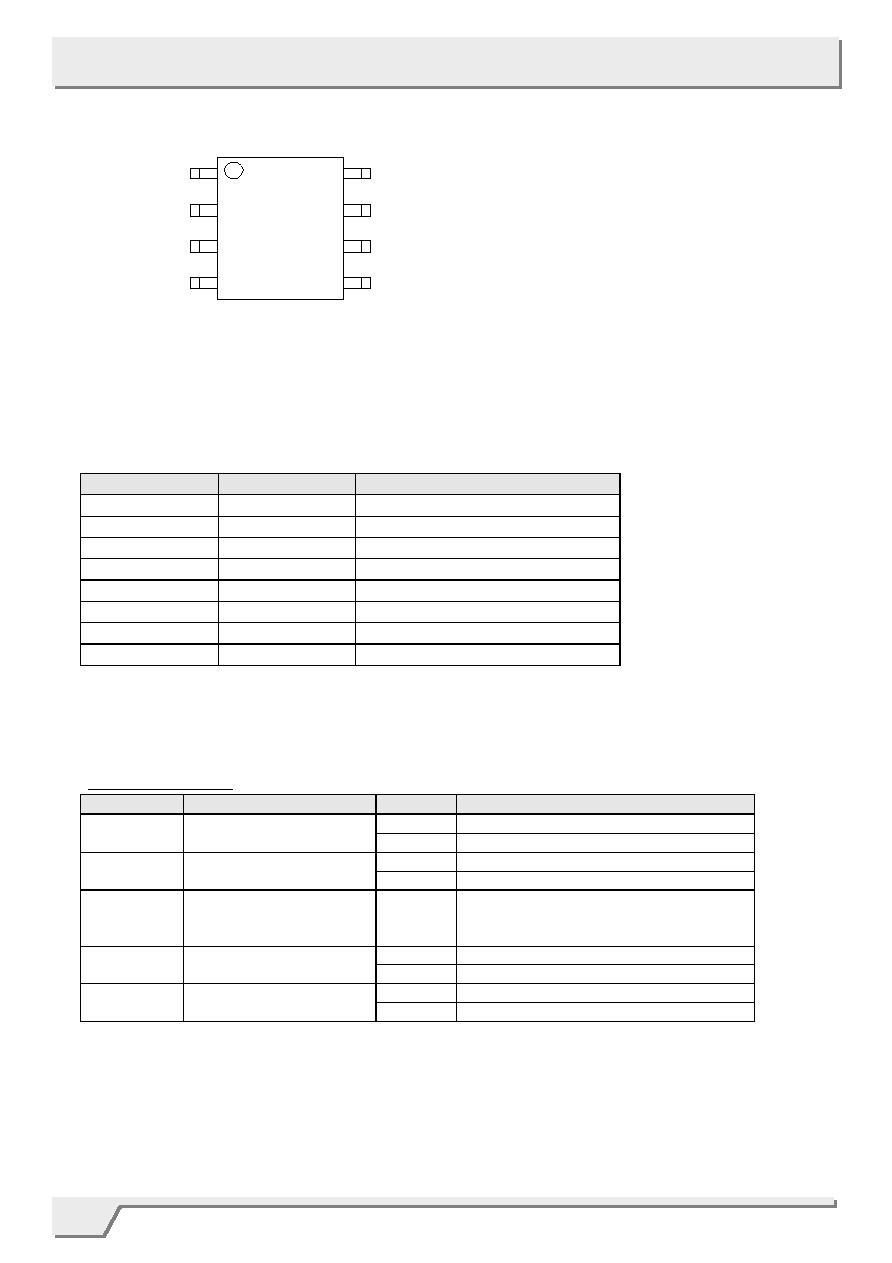
PIN CONFIGURATION
PRODUCT CLASSIFICATION
Ordering Information
XC6406
*1: Output voltage of 50mV steps is applied only for 2.85V type.
*2: T.B.D.: To be determined
PIN ASSIGNMENT
* Please connect the V
IN
pins No. 2 and No. 3 externally.
**Please connect the V
SS
pins No. 6 and No. 8 externally.
SOP-8 & SOP-8FD (TOP VIEW)
VOUT1 1
VIN 2
VIN 3
VOUT2 4
8 VSS
7 NC
6 VSS
5 NC
347
XC6406
Series
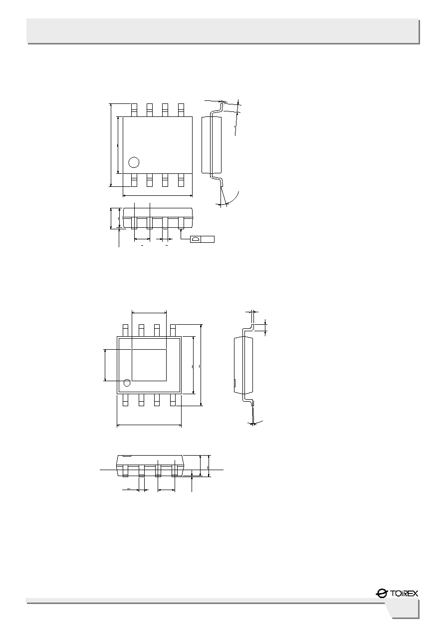
PACKAGING INFORMATION
SOP-8
SOP-8FD
(2.79)
(2.
41)
3.
9+
0.
09
6.
0+
0
.
2
0.3
5
~
1
.
0
+0.05
-0.01
0.2
4.85
+0.10
-0.05
0~
8
0.4+0.1
(1.27)
1
.
6+
0.1
3
(1.
45)
0~
0.2
5
+ 0.05
0~0.25
0.2 - 0.1
0.
4+
0.
0
4
6.
1 4.2 +
0.
4
5.0
+0.4 -0
.
3
+0.5
-0.2
0~
10
O
1.27+0.03
0.4+0.1
0.10
-0
.
1
8
+0.
1
5
1.
5
8
1.5+0.
1

348
XC6406
Series
MARK
PRODUCT SERIES
0 6
XC6406****S*
MARK
VOLTAGE(V)
VR1
VR2
PRODUCT SERIES
0 1 3.3
2.5
XC6406**01S*
MARK
PRODUCTION YEAR
3 2003
4 2004
MARK
PRODUCTION LOT NUMBER
- 3
03
0 1
1A
MARK
VR1REGULATOR TYPE
PRODUCT SERIES
P Short-Circuit
Protection
Circuit Built-In
XC6406P***S*
E
No Current Limiter Circuit Built-In
XC6406E***S*
MARK
VR2REGULATOR TYPE
PRODUCT SERIES
P Short-Circuit
Protection
Circuit Built-In
XC6406P***S*
E
No Current Limiter Circuit Built-In
XC6406E***S*
MARKING RULE
Represents product series
Represents type of VR1 regulator
Represents type of VR2 regulator
Represents production lot number
0 to 9, A to Z repeated(G,I,J,O,Q,W excepted)
Note: No character inversion used.
ex)
Represents VR output voltage
ex)
Represents a least significant digit of production year
ex)
SOP-8
SOP-8
(TOP VIEW)
1
2
3
4
8
7
6
5
349
XC6406
Series
PARAMETER
SYMBOL
RATINGS
UNITS
Input Voltage
V
IN
10
V
Output Current
I
OUT
1 + I
OUT
2 600 mA
Output Voltage
V
OUT
1 / 2
V
SS
≠ 0.3 ~ V
IN
+ 0.3
V
EN Pin Voltage
V
EN
1 / 2
V
SS
≠ 0.3 ~ V
IN
+ 0.3
V
SOP-8 300
Power Dissipation
SOP-8FD
Pd
300
mW
Operating Temperature Range
Topr
- 40 ~ + 85
Storage Temperature Range
Tstg
- 55 ~ + 125
PARAMETER
SYMBOL
CONDITIONS
MIN.
TYP.
MAX.
UNITS
Supply Current
I
DD
V
IN
=7V
-
20
40
A
Input Voltage
V
IN
-
-
8.0
V
PARAMETER
SYMBOL
CONDITIONS
MIN.
TYP.
MAX.
UNITS
Output Voltage (*2)
V
OUT
(E) V
IN
=2.8V, I
OUT
=40mA 1.764
1.800
V
OUT
(T)
1.836 V
Maximum Output Current
I
OUT
MAX V
IN
=2.8V, V
OUT
V
OUT
(E) x 0.9
400
-
-
mA
Load Regulation
V
OUT
V
IN
=2.8V, 1mAI
OUT
200mA - 40
100
mV
Vdif1 I
OUT
=100mA -
200
300
mV
Dropout Voltage (*3)
Vdif2 I
OUT
=200mA -
400
600
MV
V
OUT
Line Regulation
V
IN
V
OUT
2.8VV
IN
8.0V, I
OUT
=40mA
-
0.2
0.3
% / V
V
OUT
Output Voltage
Temperature Range
ToprV
OUT
I
OUT
=40mA, -40Topr85 -
±100 -
ppm
/
ABSOLUTE MAXIMUM RATINGS
Ta = 25
ELECTRICAL CHARACTERISTICS
XC6406EExx
* Please connect the V
IN
pins No. 2 and No. 3 externally.
**Please connect the V
SS
pins No. 6 and No. 8 externally
V
OUT
(T) = 1.8V
Ta=25
NOTE:
*1: V
OU
T(T) : Specified output voltage
*2: V
OUT
(E) : Effective output voltage
(I.e. the output voltage when "V
OUT
(T)+1.0V" is provided at the V
IN
pin while maintaining a certain I
OUT
.)
*3: Vdif={V
IN
1
(*5)
- V
OUT
1
(*4)
}
*4: V
OUT
1: A voltage equal to 98% of the output voltage whenever an amply stabilized V
OUT
1=I
OUT
{V
OUT
(T)+1.0V} is input.
*5: V
IN
1=The input voltage when V
OUT
1 appears as input voltage is gradually decreased.