PFM Controlled,StepUp DC/DC Converter +Multi Voltage Detector
Series
669
10
The XC651A series are step-up DC/DC converter and multi voltage detector IC s.
CMOS processes and laser trimming technology provide high accuracy and low power
consumption.
The XC651A comprises of a PFM controlled step-up DC/DC converter, a voltage
detector with 4 x 5 level window comparators built-in, plus 2 other voltage detectors.
The step-up DC/DC converter's EN pin ( chip enable ) provides power consumption
savings when the step-up operations are not operating ( stand-by mode ).
The series is available in a small TSSOP-16 package.
General Description
Independent power supply for each built-in block :
Each of the following built-in blocks is operated by a separate power supply :
PFM controlled, step-up DC/DC converter ( PFM DC/DC )
5 level window comparator ( MWVD )
Negative Logic : XC651A3 Series
Positive Logic : XC651A4 Series
Voltage detector 1 with built-in delay circuit ( VD1 )
Voltage detector 2 ( VD2 )
Highly accurate set-up voltage :
PFM controlled, step-up DC/DC converter : set-up voltage accuracy ±2.5%
5 level window comparator : set-up voltage accuracy ±2%
Voltage detectors 1, 2 : set-up voltage accuracy ±2%
Set-up voltage range :
PFM controlled, step-up DC/DC converter : 2.0V ~ 3.0V ( selectable in 0.1V steps)
5 level window comparator : 1.1V ~ 2.5V * ( selectable in 0.1V steps )
Voltage detectors 1, 2 : 0.9V ~ 3.0V ( selectable in 0.1V steps )
Operational voltage range :
0.9V ~ 6.0V
Small Package :
TSSOP-16
* Note :
The set-up voltage of the 5 level window comparator cannot be freely set-up due to the limitations of the circuit.
Please also note that the set-up voltage range of MWVD1 is 1.0V ~ 1.8V.
GBattery Powered Equipment
GVarious Portable Equipment
Features
Applications
NCMOS Low Power Consumption
NPFM Controlled, Step-Up DC/DC Converter
N5 Level Window Comparator
NVoltage Detector × 2 ( Independent Power
Supply )
NTSSOP-16 Package
10S_02XC651A 02.09.12 15:38 669

XC651A
Series
670
10
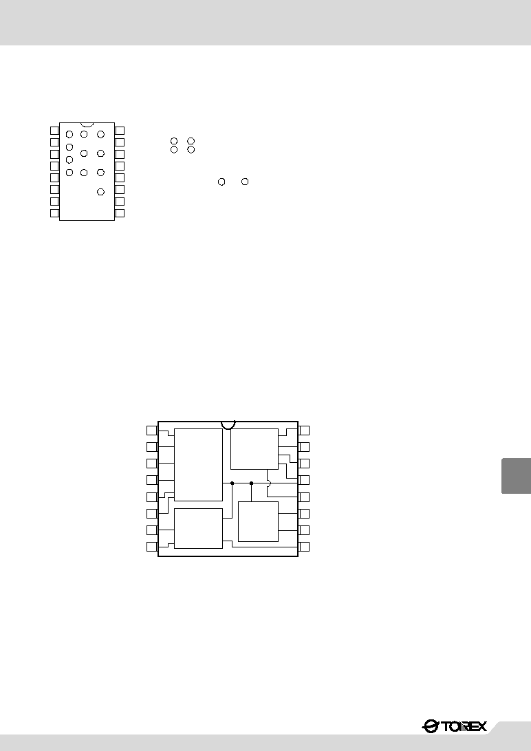
Pin Configuration
Pin Assignment
1
2
MWVD
IN
RIP
3
4
MW
OUT1
5
6
7
8
CD
16
15
V
OUT
14
13
12
11
10
9
TSSOP-16
TOP VIEW
MW
OUT2
MW
OUT3
MW
OUT4
V
IN1
EXT
L
X
V
SS
EN
V
IN2
V
DET2
V
DET1
PIN NUMBER
PIN NAME
1
MWVD
IN
MWVD detect, MWVD current
2
RIP
MWVD ripple exclusion capacitor connection
3
MW
OUT1
MWVD output 1
4
MW
OUT2
MWVD output 2
5
MW
OUT3
MWVD output 3
6
MW
OUT4
MWVD output 4
7
CD
VD1 delay time set-up capacitor connection
8
V
IN1
VD1 detect, VD1 current
9
V
DET1
VD1 output
10
V
DET2
VD2 output
11
V
IN2
VD2 detect, VD2 current
12
EN
DC/DC enable
13
V
SS
Ground pin ( common )
14
Lx
DC/DC built-in transistor switch output
15
EXT
DC/DC external transistor drive output
16
V
OUT
DC/DC output voltage monitor, DC/DC current
FUNCTION
Packaging Information
GTSSOP-16
Product Classification
GOrdering Information
e
Em bossed Tape (Right)
Em bossed Tape (Left)
q
DESCRIPTION
SYMBOL
DESCRIPTION
SYMBOL
w
q
w e
Voltage Characteristics :
Based on internal standards
Package Type
-
Device Orientation
D
C
y
b
e
A1
A2
A
L
E1
E
SIZE mm
MIN
TYP
MAX
A
A1
A2
b
C
D
E
E1
e
L
y
0.03
0.95
0.15
0.12
4.9
6.20
4.30
0.40
0.07
1.10
0.10
1.05
0.30
0.22
0.17
0.22
5.30
5.10
6.40
6.60
4.50
4.40
0.65
0.50
0.60
0.10
10S_02XC651A 02.09.12 15:38 670
XC651A
Series
672
10
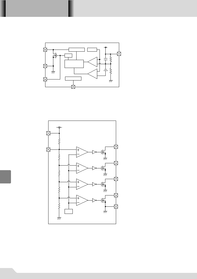
L
X
EXT
EN
V
OUT
V
LX
Limit
2step PFM Control
OSC
Buffer
DC/DC Enable
V
DD
Vref
+
-
+
-
V
SS
Note 1
Note 2
V
DD
MWVD
IN
RIP
R
RIP
Vref
Note 1
Note 2
V
SS
MW
OUT1
MW
OUT2
MW
OUT3
MW
OUT4
Note 3
Note 3
Note 3
Note 3
2) PFM DC/DC
3) MWVD
Note 1 : The V
SS
pin is common to each block.
Note 2 : V
DD
is independent for each block.
Note 1 : The V
SS
pin is common to each block.
Note 2 : V
DD
is independent for each block.
Note 3 : Applies to the XC6514 Series (Positive Logic) only.
10S_02XC651A 02.09.12 15:38 672